


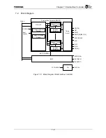


Chapter 7 External Bus Controller
7-6
7.3.4 External
Address
Output
The maximum memory space size for each channel is 1 GB (230B). Addresses are output by dividing
the 20-bit ADDR[19:0] signal into two parts: the upper address and the lower address. The address bit
output to each bit of the ADDR[19:0] signal changes according to the setting of the channel data bus
width. (See “7.3.5 Data Bus Size” for more information.)
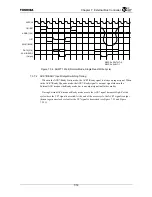
It is possible for an external device to latch the upper eight address bits using the ACE* signal. Either
the ACE* signal itself can be used as a Latch Enable signal or the upper address can be latched at the
rise of SYSCLK when the ACE* signal is being asserted.
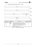
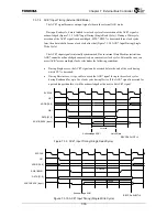
The ADDR signal output is held for one clock cycle after the ACE* signal rise when the
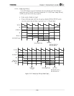
CCFG.ACEHOLD bit is set (default). (See Figure 7.5.1.) The ADDR signal output is not held when the
CCFG.ACEHOLD bit is cleared. This hold time setting is applied globally to all channels.
The ACE* signal of the upper address is always asserted at the first external bus access cycle after
Reset. In all subsequent external bus access cycles, the bit mapping of the upper address output to
ADDR[19:12] is compared to the bit mapping of the upper address output to ADDR[19:12] previously.
The upper address is output and the ACE* signal is asserted only if the compared results do not match.
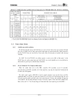
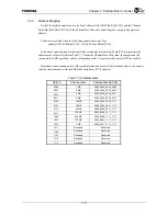
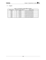
As indicated below in Table 7.3.3, in the case of channel sizes that do not use the upper address
latched by the ACE* signal, with the exception of the first cycle after reset, the upper address is not
output and the ACE* signal is not asserted.
Table 7.3.3 Relationship Between the Upper Address Output and the Channel Size (CS)
CS
Bus Width
1 MB
2 MB
4 MB
8 MB or more
32 bits
⎯
⎯
⎯
√
16 bits
⎯
⎯
√
√
8 bits
⎯
√
√
√
√
: The upper address output changes when the upper address changes.
⎯
: The upper address output does not change (with the exception of the first cycle after
reset.)
Содержание TX49 TMPR4937
Страница 1: ...64 Bit TX System RISC TX49 Family TMPR4937 Rev 2 0 ...
Страница 4: ......
Страница 13: ...Table of Contents ix TMPR4937 Revision History 1 ...
Страница 14: ...Table of Contents x ...
Страница 15: ...Handling Precautions ...
Страница 16: ......
Страница 18: ...1 Using Toshiba Semiconductors Safely 1 2 ...
Страница 40: ...3 General Safety Precautions and Usage Considerations 3 18 ...
Страница 42: ...4 Precautions and Usage Considerations 4 2 ...
Страница 43: ...TMPR4937 2005 3 Rev 2 0 ...
Страница 44: ......
Страница 52: ...Chapter 1 Overview and Features 1 6 ...
Страница 156: ...Chapter 7 External Bus Controller 7 56 ...
Страница 491: ...Chapter 16 Removed 16 1 16 Removed ...
Страница 492: ...Chapter 16 Removed 16 2 ...
Страница 493: ...Chapter 17 Removed 17 1 17 Removed ...
Страница 494: ...Chapter 17 Removed 17 2 ...
Страница 495: ...Chapter 18 Removed 18 1 18 Removed ...
Страница 496: ...Chapter 18 Removed 18 2 ...
Страница 497: ...Chapter 19 Removed 19 1 19 Removed ...
Страница 498: ...Chapter 19 Removed 19 2 ...
Страница 506: ...Chapter 20 Extended EJTAG Interface 20 8 ...
Страница 529: ...Chapter 22 Pinout and Package Information 22 9 22 2 Package Dimensions P BGA484 3535 1 27B9 Unit mm ...
Страница 530: ...Chapter 22 Pinout and Package Information 22 10 ...
Страница 542: ...Chapter 24 Parts Number when Ordering 24 2 ...
Страница 544: ...Appendix A TX49 H3 Core Supplement A 2 ...


