


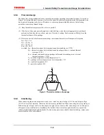


3 General Safety Precautions and Usage Considerations
3-7
CMOS logic IC inputs, for example, have extremely high impedance. If an input pin is left open, it can easily
pick up extraneous noise and become unstable. In this case, if the input voltage level reaches an intermediate
level, it is possible that both the P-channel and N-channel transistors will be turned on, allowing unwanted
supply current to flow. Therefore, ensure that the unused input pins of a device are connected to the power
supply (Vcc) pin or ground (GND) pin of the same device. For details of what to do with the pins of heat sinks,
refer to the relevant technical datasheet and databook.
3.3.5 Latch-up
Latch-up is an abnormal condition inherent in CMOS devices, in which Vcc gets shorted to ground. This
happens when a parasitic PN-PN junction (thyristor structure) internal to the CMOS chip is turned on, causing a
large current of the order of several hundred mA or more to flow between Vcc and GND, eventually causing the
device to break down.
Latch-up occurs when the input or output voltage exceeds the rated value, causing a large current to flow in the
internal chip, or when the voltage on the Vcc (Vdd) pin exceeds its rated value, forcing the internal chip into a
breakdown condition. Once the chip falls into the latch-up state, even though the excess voltage may have been
applied only for an instant, the large current continues to flow between Vcc (Vdd) and GND (Vss). This causes
the device to heat up and, in extreme cases, to emit gas fumes as well. To avoid this problem, observe the
following precautions:
(1) Do not allow voltage levels on the input and output pins either to rise above Vcc (Vdd) or to fall below
GND (Vss). Also, follow any prescribed power-on sequence, so that power is applied gradually or in steps
rather than abruptly.
(2) Do not allow any abnormal noise signals to be applied to the device.
(3) Set the voltage levels of unused input pins to Vcc (Vdd) or GND (Vss).
(4) Do not connect output pins to one another.
3.3.6 Input/Output
protection
Wired-AND configurations, in which outputs are connected together, cannot be used, since this short-circuits the
outputs. Outputs should, of course, never be connected to Vcc (Vdd) or GND (Vss).
Furthermore, ICs with tri-state outputs can undergo performance degradation if a shorted output current is
allowed to flow for an extended period of time. Therefore, when designing circuits, make sure that tri-state
outputs will not be enabled simultaneously.
3.3.7 Load
capacitance
Some devices display increased delay times if the load capacitance is large. Also, large charging and discharging
currents will flow in the device, causing noise. Furthermore, since outputs are shorted for a relatively long time,
wiring can become fused.
Consult the technical information for the device being used to determine the recommended load capacitance.
Содержание TX49 TMPR4937
Страница 1: ...64 Bit TX System RISC TX49 Family TMPR4937 Rev 2 0 ...
Страница 4: ......
Страница 13: ...Table of Contents ix TMPR4937 Revision History 1 ...
Страница 14: ...Table of Contents x ...
Страница 15: ...Handling Precautions ...
Страница 16: ......
Страница 18: ...1 Using Toshiba Semiconductors Safely 1 2 ...
Страница 40: ...3 General Safety Precautions and Usage Considerations 3 18 ...
Страница 42: ...4 Precautions and Usage Considerations 4 2 ...
Страница 43: ...TMPR4937 2005 3 Rev 2 0 ...
Страница 44: ......
Страница 52: ...Chapter 1 Overview and Features 1 6 ...
Страница 156: ...Chapter 7 External Bus Controller 7 56 ...
Страница 491: ...Chapter 16 Removed 16 1 16 Removed ...
Страница 492: ...Chapter 16 Removed 16 2 ...
Страница 493: ...Chapter 17 Removed 17 1 17 Removed ...
Страница 494: ...Chapter 17 Removed 17 2 ...
Страница 495: ...Chapter 18 Removed 18 1 18 Removed ...
Страница 496: ...Chapter 18 Removed 18 2 ...
Страница 497: ...Chapter 19 Removed 19 1 19 Removed ...
Страница 498: ...Chapter 19 Removed 19 2 ...
Страница 506: ...Chapter 20 Extended EJTAG Interface 20 8 ...
Страница 529: ...Chapter 22 Pinout and Package Information 22 9 22 2 Package Dimensions P BGA484 3535 1 27B9 Unit mm ...
Страница 530: ...Chapter 22 Pinout and Package Information 22 10 ...
Страница 542: ...Chapter 24 Parts Number when Ordering 24 2 ...
Страница 544: ...Appendix A TX49 H3 Core Supplement A 2 ...


