RX610 Group
11. Buses
R01UH0032EJ0120 Rev.1.20
Page 295 of 1006
Feb 20, 2013
11.5.3
Insertion of Recovery Cycles
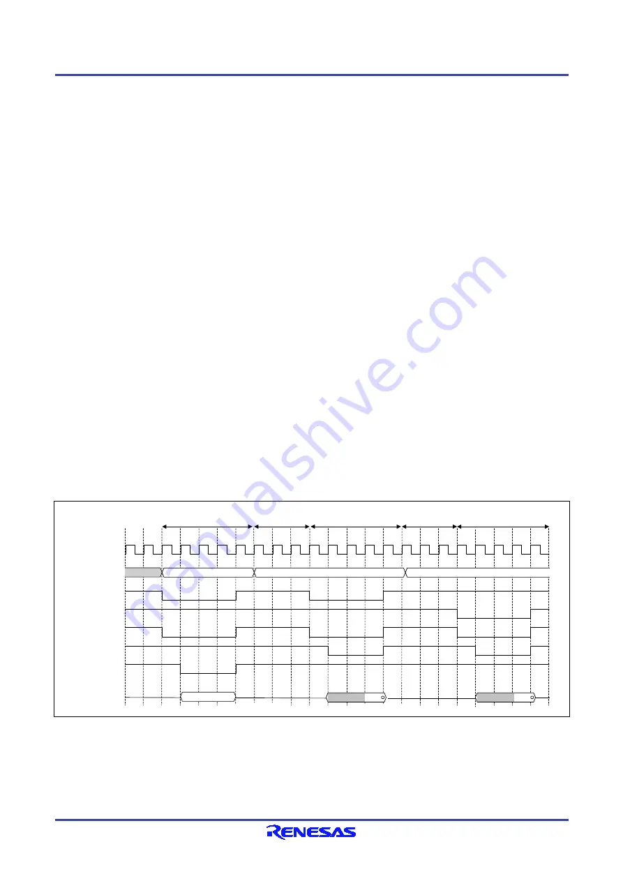
Clock cycles of recovery can be inserted between consecutive rounds of external bus access. Conditions where cycles of
recovery can be inserted are described below.
•
Write access via the external bus follows read access via the external bus.
•
Read access via the external bus follows read access to a different area via the external bus.
•
Read access via the external bus follows write access via the external bus.
Clock cycles of recovery are not inserted between write access and subsequent write access.
Separate numbers of clock cycles for recovery can be set up for insertion after cycles of reading or writing. The number
of bus-clock cycles to be inserted for recovery following a write cycle is set by the WRCV[3:0] bits in CSiREC for the
area to which a write access has been performed in the preceding bus cycle, and the number of bus-clock cycles to be
inserted as the recovery cycle that follows a read cycle is set by the RRCV[3:0] bits in CSiREC for the area to which a
read access has been performed in the preceding bus cycle. In other words, when a read access is made to CS0 and then
to CS1, the number of recovery cycles to be inserted between these two accesses is determined by the PRCV[3:0] bits in
CS0REC.
The clock cycles of recovery begin at the end of the preceding bus cycle, i.e. when the CSi# signal (i = 0 to 7) is negated.
From this point, the selected period over which the CSi# signal is at the high level (i.e. the recovery period) is inserted.
After the end of the clock cycles of recovery, the CSi# signal is asserted for the next round of bus access after the
insertion of no less than one bus-clock cycle as an idle cycle. Even if the next request for access to an external address
space is generated during the recovery period, the next round of access over the external bus will only start after one
bus-clock cycle has been inserted as an idle cycle following the end of the recovery period.
Chip select 0
(CS0#)
Data write
(WR0#, WR1#, WR#)
Chip select 1
(CS1#)
A0
A1
A2
D0
CS0 write
Write recovery
(CS0REC.WRCV[3:0]: 3)
CS0 read
Write recovery
(CS0REC.RRCV[3:0]: 3)
CS1 read
Tw1
Tw2
Tw3
Tend
Tw1
Tw2
Tw3
Tend
Th
Tw1
Tw2
Tw3
Tend
Byte control
(BC0#, BC1#)
D1
D2
Tr1
Tr2
Tr3
Th
Th
Tr1
Tr2
Tr3
Data bus
(D15 to D0)
External bus clock
(BCLK)
Address
(A23 to A0)
Data read
(RD#)
Figure 11.21 Example of Recovery Timing


