


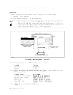


Active
Channel:
CH
1
4
Ch
1
5
Data
Math:
D
A
T
A+MEM
4
Displa
y
5,
NNNNNNNNNNNNNNNNNNNNNNNNNNNNNNNNNNNNNNNNNNNNNNN
DATA
MATH
[xxx]
,
NNNNNNNNNNNNNNNNNNNNNNNNNN
DATA+MEM
,
NNNNNNNNNNNNNN
GAIN
,
4
.
5,
4
5
5,
4
x1
5
Auto
Scale
4
Scale
Ref
5,
NNNNNNNNNNNNNNNNNNNNNNNNNNNNNNNN
AUTO
SCALE
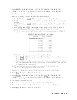
Active
Channel:
CH
2
4
Ch
2
5
Data
Math:
D
A
T
A+MEM
4
Displa
y
5,
NNNNNNNNNNNNNNNNNNNNNNNNNNNNNNNNNNNNNNNNNNNNNNN
DATA
MATH
[xxx]
,
NNNNNNNNNNNNNNNNNNNNNNNNNN
DATA+MEM
,
NNNNNNNNNNNNNN
GAIN
,
4
.
5,
4
5
5,
4
x1
5
Auto
Scale
4
Scale
Ref
5,
NNNNNNNNNNNNNNNNNNNNNNNNNNNNNNNN
AUTO
SCALE
Press
4
Ch
1
5,
4
Search
5,
NNNNNNNNNNN
MAX
and
4
Search
5,
NNNNNNNNNNN
MIN
to
mov
e
the
c
hannel
1
marker
to
the
maximum
and
minimum
p oints
on
the
trace.
Compare
the
absolute
v
alues
at
the
maximum
and
minimum
p oints.
Record
the
larger
v
alue
in
the
p erformance
test
record
(\T
est
Result"
column
for
A/R
magnitude
ratio).
Press
4
Ch
2
5,
4
Ma
rk
er !
5,
NNNNNNNNNNNNNNNNNNNNNNNNNNNNN
MKR !STOP
,
4
Cal
5,
NNNNNNNNNNNNNN
MORE
,
NNNNNNNNNNNNNNNNNNNNNNNNNNNNNNNNNNNNNNNNNNNNNNNNNNNNNNNNNNNNNNNNN
ELECTRICAL
DELAY
MENU
,
NNNNNNNNNNNNNNNNNNNNNNNNNNNNNNNN
MKR !DELAY
,
NNNNNNNNNNNNNNNNNNNNNNNNNNNNNNNNNNNNNNNNNNNNNNNNNN
ELECTRICAL
DELAY
.
Then
press
4
*
5
or
4
+
5
and
turn
the
RPG
knob
to
v
ary
the
electrical
dela
y
un
til
the
trace
is
in
the
most
horizontal
p osition.
Press
NNNNNNNNNNNNNNNNNNNNNNNNNNNNNNNNNNNNNN
PHASE
OFFSET
and
en
ter
the
trace
mean
v
alue
using
n
umeric
k
eys.
The
trace
mean
v
alue
is
display
ed
as
a
marker
statistic
(mean)
in
the
upp er
right-hand
corner
of
the
display
.
Press
4
Search
5,
NNNNNNNNNNN
MAX
and
4
Search
5,
NNNNNNNNNNN
MIN
to
mov
e
the
c
hannel
2
marker
to
the
maximum
and
minimum
p oints
on
the
trace.
Compare
the
absolute
v
alues
at
the
maximum
and
minimum
p oints.
Record
the
larger
v
alue
in
the
p erformance
test
record
(\T
est
Result"
column
for
A/R
phase).
P
erformance
T
ests
2-49
Summary of Contents for 4395A
Page 10: ......
Page 26: ......
Page 34: ......
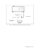
Page 77: ...Figure 2 17 B R Magnitude Ratio Phase Dynamic Accuracy Test Setup 2 Performance Tests 2 43 ...
Page 167: ...Figure 5 1 Adjustment Hardware Setup Adjustments 5 5 ...
Page 186: ...Figure 5 13 Receiver Gain Adjustment Location 5 24 Adjustments ...
Page 190: ...Figure 5 16 Receiver Flatness Adjustment Setup 1 MHz 5 28 Adjustments ...
Page 194: ...Figure 5 20 DC Bias Adjustment Setup 2 5 32 Adjustments ...
Page 196: ...Figure 6 1 Troubleshooting Organization 6 2 Troubleshooting ...
Page 206: ...Figure 7 1 Power Supply Lines Simplified Block Diagram 7 2 Power Supply Troubleshooting ...
Page 212: ...Figure 7 5 A1 CPU Connector Locations 7 8 Power Supply Troubleshooting ...
Page 220: ...Figure 8 1 Digital Control Group Simplified Block Diagram 8 2 Digital Control Troubleshooting ...
Page 240: ...Figure 10 1 Top View Major Assemblies 10 4 Replaceable Parts ...
Page 292: ...Table A 2 Manual Changes by Firmware Version Version Make Manual Changes A 2 Manual Changes ...
Page 308: ......
Page 311: ...Figure B 1 Power Cable Supplied Power Requirement B 3 ...
Page 312: ......
Page 342: ......


