


16.4.7 ADCMPCR1(Monitoring Setting Register 1)
After fixing the conversion result, the interrupt signal (INTADCP) is generated.
31
30
29
28
27
26
25
24
bit symbol
-
-
-
-
-
-
-
-
After reset
0
0
0
0
0
0
0
0
23
22
21
20
19
18
17
16
bit symbol
-
-
-
-
-
-
-
-
After reset
0
0
0
0
0
0
0
0
15
14
13
12
11
10
9
8
bit symbol
-
-
-
-
CMPCNT1
After reset
0
0
0
0
0
0
0
0
7
6
5
4
3
2
1
0
bit symbol
CMP1EN
-
-
ADBIG1
REGS1
After reset
0
0
0
0
0
0
0
0
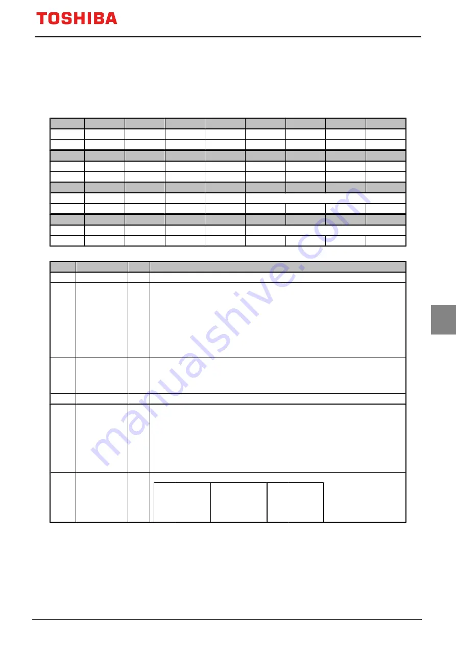
Bit
Bit Symbol
Type
Function
31-12
-
R
Read as "0".
11-8
CMPCNT1[3:0]
R/W
Comparison count for determining the result
0: After every comparison
1: After two comparisons
・
・
15: After 16 comparisons
The ADCMPCR0 and ADCMPCR1 registers are used to enable or disable comparison between an AD
conversion result and the specified comparison value, to select the register to be compared with an AD
conversion result and to set how many times comparison should be performed to determine the result.
7
CMP1EN
R/W
Monitoring function
0:Disable
1:Enable
By setting <CMP1EN>="0"(disable), accumulated number of decision counts is cleared.
6-5
-
R
Read as "0".
4
ADBIG1
R/W
Comparison condition
0:Larger than or equal to compare register
1:Smaller than or equal to compare register
Compares whether a result of analog input is larger or smaller than the compare register.
Every time AD conversion, which is set in the <REGS1[3:0]>, is complete, large/small decision is per-
formed.
If the result is matched the setting in <ADBIG1>, the counter increments.
3-0
REGS1[3:0]
R/W
AD conversion result register to be compared
0000: ADREG0
0100: ADREG4
1000: ADREG8
0001: ADREG1
0101: ADREG5
1001: ADREG9
0010: ADREG2
0110: ADREG6
1010: ADREG10
0011: ADREG3
0111: ADREG7
1011: ADREG11
TMPM3V6/M3V4
Page 365
2019-02-06
Summary of Contents for TMPM3V4
Page 1: ...32 Bit RISC Microcontroller TX03 Series TMPM3V6 M3V4 ...
Page 2: ... 2019 Toshiba Electronic Devices Storage Corporation ...
Page 7: ...Revision History Date Revision Comment 2019 02 06 1 First Release ...
Page 8: ......
Page 22: ...xiv ...
Page 52: ...TMPM3V6 M3V4 3 Processor Core 3 6 Exclusive access Page 30 2019 02 06 ...
Page 148: ...TMPM3V6 M3V4 7 Exceptions 7 6 Exception Interrupt Related Registers Page 126 2019 02 06 ...
Page 178: ...TMPM3V6 M3V4 9 Input Output port 9 2 Block Diagrams of Ports Page 156 2019 02 06 ...
Page 354: ...TMPM3V6 M3V4 14 Synchronous Serial Port SSP 14 6 Frame Format Page 332 2019 02 06 ...
Page 419: ...TMPM3V6 M3V4 Page 397 2019 02 06 ...
Page 462: ...TMPM3V6 M3V4 21 Watchdog Timer WDT 21 5 Control register Page 440 2019 02 06 ...
Page 544: ......


