12-6
MC9328MX1 Reference Manual
MOTOROLA
Phase-Locked Loop and Clock Controller
CSCR
Clock Source Control Register
Addr
0x0021B000
BIT
31
30
29
28
27
26
25
24
23
22
21
20
19
18
17
16
CLKO_SEL
USB_DIV
SD_CNT
SPLL_
RESTART
MPLL_
RESTART
CLK16
_SEL
OSC
_EN
System
_SEL
TYPE
rw
rw
rw
rw
rw
rw
rw
rw
r
rw
rw
r
r
rw
rw
rw
RESET
0
0
0
0
1
1
1
1
0
0
0
0
0
0
0
0
0x0F00
BIT
15
14
13
12
11
10
9
8
7
6
5
4
3
2
1
0
PRESC
BCLK_DIV
SPEN
MPEN
TYPE
rw
r
rw
rw
rw
rw
r
r
r
r
r
r
r
r
rw
rw
RESET
1
0
1
0
1
1
0
0
0
0
0
0
0
0
1
1
0xAC03
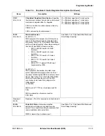
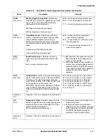
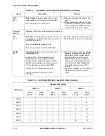
Table 12-5. Clock Source Control Register Description
Name
Description
Settings
CLKO_SEL
Bits 31
–
29
CLKO Select
—Selects the clock signal source
that is output on the CLKO pin.
000 = PERCLK1
001 = HCLK
010 = CLK48M
011 = CLK16M
100 = PREMCLK
101 = FCLK
USB_DIV
Bits 28
–
26
USB Divider
—Contains the integer divider value
used to generate the CLK48M signal for the USB
modules.
000 = System PLL clock divide by 1
001 = System PLL clock divide by 2
.
.
.
111 = System PLL clock divide by 8
SD_CNT
Bits 25
–
24
Shut-Down Control
—Contains the value that sets
the duration of System PLL clock output after 0 is
written to the SPEN bit. The power controller
requests the bus before System PLL shutdown.
Any unmasked interrupt event enables the System
PLL.
00 = System PLL shuts down after next
rising edge of CLK32 is detected and
the current bus cycle is completed. A
minimum of 16 HCLK cycles is
guaranteed from writing “0” to SPEN
bit.
01 = System PLL shuts down after the
second rising edge of CLK32 is
detected and the current bus cycle is
completed.
10 = System PLL shuts down after the third
rising edge of CLK32 is detected and
the current bus cycle is completed.
11 = System PLL shuts down after forth
rising edge of CLK32 is detected and
the current bus cycle is completed.
Reserved
Bit 23
Reserved—This bit is reserved and should read 0.
Summary of Contents for DragonBall MC9328MX1
Page 68: ...1 12 MC9328MX1 Reference Manual MOTOROLA Introduction ...
Page 86: ...2 18 MC9328MX1 Reference Manual MOTOROLA Signal Descriptions and Pin Assignments ...
Page 116: ...3 30 MC9328MX1 Reference Manual MOTOROLA Memory Map ...
Page 126: ...4 10 MC9328MX1 Reference Manual MOTOROLA ARM920T Processor ...
Page 160: ...8 8 MC9328MX1 Reference Manual MOTOROLA System Control ...
Page 272: ...13 32 MC9328MX1 Reference Manual MOTOROLA DMA Controller ...
Page 281: ...Programming Model MOTOROLA Watchdog Timer Module 14 9 ...
Page 282: ...14 10 MC9328MX1 Reference Manual MOTOROLA Watchdog Timer Module ...
Page 300: ...15 18 MC9328MX1 Reference Manual MOTOROLA Analog Signal Processor ASP ...
Page 438: ...18 16 MC9328MX1 Reference Manual MOTOROLA Serial Peripheral Interface Modules SPI 1 and SPI 2 ...
Page 478: ...19 40 MC9328MX1 Reference Manual MOTOROLA LCD Controller ...
Page 574: ...21 32 MC9328MX1 Reference Manual MOTOROLA Memory Stick Host Controller MSHC Module ...
Page 598: ...23 16 MC9328MX1 Reference Manual MOTOROLA Real Time Clock RTC ...
Page 670: ...24 72 MC9328MX1 Reference Manual MOTOROLA SDRAM Memory Controller ...
Page 726: ...25 56 MC9328MX1 Reference Manual MOTOROLA SmartCard Interface Module SIM ...
Page 736: ...26 10 MC9328MX1 Reference Manual MOTOROLA General Purpose Timers ...
Page 854: ...29 18 MC9328MX1 Reference Manual MOTOROLA I2C Module ...
Page 900: ...30 46 MC9328MX1 Reference Manual MOTOROLA Synchronous Serial Interface SSI ...
Page 942: ...32 26 MC9328MX1 Reference Manual MOTOROLA GPIO Module and I O Multiplexer IOMUX ...


