16-18
MC9328MX1 Reference Manual
MOTOROLA
Bluetooth Accelerator (BTA)
16.3.2 Wake-Up Module
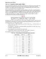
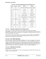
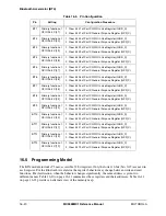
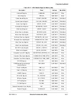
The BTA provides a wake-up module for power saving operation. Figure 16-9 shows the block diagram of
the wake-up module.
Figure 16-9. Block Diagram of the Wake-Up Module
The wake-up module consists of a wake-up counter clocked by a 32 kHz clock. The counter can be reset by
software by setting the
CLR_CNT
bit in the WU_CONTROL register.
Power-down timing can be programmed via three wake-up registers. When the software specifies a
power-down, the wake-up counts must be set up by writing to the WAKEUP_1, WAKEUP_2, and
WAKEUP_DELTA4 registers. The power-down process is then started by writing to the
PDE
bit in the
WU_CONTROL register.
All three wake-up compare registers specify wake-up times in 31.25 µs units (31.25 µs is the reciprocal of
32 kHz). The wake-up times indicate the elapsed time from when the power-down process is started
(wake-up counter is reset upon request). The wake-up events (
WU1
,
WU2
and
WU4
) are generated when
the WU_COUNT register value equals their respective wake-up compare registers.
The three wake-up compare registers are used as follows:
1. After software determines that a power-down has to be performed, the WAKEUP_1 register
specifies the delay until the BTRFOSC and BT1ClkHold signals are asserted. The assertion
of BTRFOSC signals a power-down request to the oscillator source. Immediately after the
activation of BTRFOSC (which is synchronized with the Bluetooth master clock),
BT1ClkHold is asserted. BT1ClkHold results in a synchronized hold of the Bluetooth master
clock. The actual stopping of the source clock must not happen before BT1ClkHold is
asserted.
2. The WAKEUP_2 register specifies the delay until BTRFOSC is deasserted, which is the the
actual wake-up event. Once the BTRFOSC signal is deasserted, the source clock must be
turned on.
3. The WAKEUP_4 register holds the value at which the Bluetooth clock is enabled again
(BT1ClkHold goes high). After receiving a WU2 event, WAKEUP_4 is updated with the
sum of the WU_COUNT and WAKEUP_DELTA4 registers. The WAKEUP_DELTA4 value
WakeUp_1
WakeUp_2
WakeUp_delta4
WakeUp_4
compare
compare
compare
WU_Count
+
BT1clkHold
BTRFOSC
Summary of Contents for DragonBall MC9328MX1
Page 68: ...1 12 MC9328MX1 Reference Manual MOTOROLA Introduction ...
Page 86: ...2 18 MC9328MX1 Reference Manual MOTOROLA Signal Descriptions and Pin Assignments ...
Page 116: ...3 30 MC9328MX1 Reference Manual MOTOROLA Memory Map ...
Page 126: ...4 10 MC9328MX1 Reference Manual MOTOROLA ARM920T Processor ...
Page 160: ...8 8 MC9328MX1 Reference Manual MOTOROLA System Control ...
Page 272: ...13 32 MC9328MX1 Reference Manual MOTOROLA DMA Controller ...
Page 281: ...Programming Model MOTOROLA Watchdog Timer Module 14 9 ...
Page 282: ...14 10 MC9328MX1 Reference Manual MOTOROLA Watchdog Timer Module ...
Page 300: ...15 18 MC9328MX1 Reference Manual MOTOROLA Analog Signal Processor ASP ...
Page 438: ...18 16 MC9328MX1 Reference Manual MOTOROLA Serial Peripheral Interface Modules SPI 1 and SPI 2 ...
Page 478: ...19 40 MC9328MX1 Reference Manual MOTOROLA LCD Controller ...
Page 574: ...21 32 MC9328MX1 Reference Manual MOTOROLA Memory Stick Host Controller MSHC Module ...
Page 598: ...23 16 MC9328MX1 Reference Manual MOTOROLA Real Time Clock RTC ...
Page 670: ...24 72 MC9328MX1 Reference Manual MOTOROLA SDRAM Memory Controller ...
Page 726: ...25 56 MC9328MX1 Reference Manual MOTOROLA SmartCard Interface Module SIM ...
Page 736: ...26 10 MC9328MX1 Reference Manual MOTOROLA General Purpose Timers ...
Page 854: ...29 18 MC9328MX1 Reference Manual MOTOROLA I2C Module ...
Page 900: ...30 46 MC9328MX1 Reference Manual MOTOROLA Synchronous Serial Interface SSI ...
Page 942: ...32 26 MC9328MX1 Reference Manual MOTOROLA GPIO Module and I O Multiplexer IOMUX ...


