Memory Stick Command Register
MOTOROLA
Memory Stick Host Controller (MSHC) Module
21-23
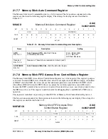
21.7.10 Memory Stick DMA Request Control Register
The Memory Stick DMA Request Control Register (MSDRQC) is a 16-bit register. The bit position
assignments for MSDRQC are shown in the following register display. The settings for this register are
described in Table 21-17 on page 21-24.
This register is initialized on power up or when RST bit of Memory Stick Control/Status Register is 1.
When the DMA controller is used with the MSHC module, the DMAC Burst Length register value must be
either 2 bytes or 8 bytes, because that MSHC module’s FIFO depth is 4 half-words (8 bytes) and the user
can configure a DMA request condition either 1 half-word or 4 half-words. The following describes the
MSHC module’s DMA request operation in a special case.
When MSRDATA is transferred out by DMA Controller and the last burst data is less than the DMAC
Burst Length register’s value, then MSHC module generates a DMA request signal for the last burst
transfer when receive a last byte data on the Read type TPC. This DMA request capability is needed to
communicate with DMA Controller.
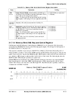
Table 21-16. Memory Stick Serial Clock Divider Register Description
Name
Description
Setting
SRC
Bit 15
Source Clock of Divider
—Selects whether the SCLKI pin or
the internal HCLK will be the source clock of the divider. This bit
must not be set to 1 during normal operation.
Note:
The SRC bit is NOT reset by setting the RST bit of the
MSCS register. A DIV setting of 00 is not supported when SRC
= 0.
0 = Select HCLK as source clock
1 = Reserved
Reserved
Bits 14–2
Reserved—These bits are reserved and should read 0.
DIV
Bits 1–0
Divide Ratio
—Selects the divide ratio. The divider supports 2
n
divide ratio, where N = 0,1,2,3. This bit must not be written after
set MSCEN bit to 1. This bit must be modified only when
MSCEN bit is 0(disabled).
Note:
The DIV bits are NOT reset by setting the RST bit of
the MSCS register. A DIV setting of 00 is not supported when
SRC = 0.
Note:
SRC = 0 and N = 0 (divide by 1) are used only for
debugging purposes.
00 = Divide by 1
01 = Divide by 2
10 = Divide by 4
11 = Divide by 8
MSDRQC
Memory Stick DMA Request Control
Register
Addr
0x0021A012
BIT
15
14
13
12
11
10
9
8
7
6
5
4
3
2
1
0
DRQEN
RFF
TFE
TYPE
rw
r
r
r
r
r
r
r
r
r
r
rw
r
r
r
rw
RESET
0
0
0
0
0
0
0
0
0
0
0
0
0
0
0
0
0x0000
Summary of Contents for DragonBall MC9328MX1
Page 68: ...1 12 MC9328MX1 Reference Manual MOTOROLA Introduction ...
Page 86: ...2 18 MC9328MX1 Reference Manual MOTOROLA Signal Descriptions and Pin Assignments ...
Page 116: ...3 30 MC9328MX1 Reference Manual MOTOROLA Memory Map ...
Page 126: ...4 10 MC9328MX1 Reference Manual MOTOROLA ARM920T Processor ...
Page 160: ...8 8 MC9328MX1 Reference Manual MOTOROLA System Control ...
Page 272: ...13 32 MC9328MX1 Reference Manual MOTOROLA DMA Controller ...
Page 281: ...Programming Model MOTOROLA Watchdog Timer Module 14 9 ...
Page 282: ...14 10 MC9328MX1 Reference Manual MOTOROLA Watchdog Timer Module ...
Page 300: ...15 18 MC9328MX1 Reference Manual MOTOROLA Analog Signal Processor ASP ...
Page 438: ...18 16 MC9328MX1 Reference Manual MOTOROLA Serial Peripheral Interface Modules SPI 1 and SPI 2 ...
Page 478: ...19 40 MC9328MX1 Reference Manual MOTOROLA LCD Controller ...
Page 574: ...21 32 MC9328MX1 Reference Manual MOTOROLA Memory Stick Host Controller MSHC Module ...
Page 598: ...23 16 MC9328MX1 Reference Manual MOTOROLA Real Time Clock RTC ...
Page 670: ...24 72 MC9328MX1 Reference Manual MOTOROLA SDRAM Memory Controller ...
Page 726: ...25 56 MC9328MX1 Reference Manual MOTOROLA SmartCard Interface Module SIM ...
Page 736: ...26 10 MC9328MX1 Reference Manual MOTOROLA General Purpose Timers ...
Page 854: ...29 18 MC9328MX1 Reference Manual MOTOROLA I2C Module ...
Page 900: ...30 46 MC9328MX1 Reference Manual MOTOROLA Synchronous Serial Interface SSI ...
Page 942: ...32 26 MC9328MX1 Reference Manual MOTOROLA GPIO Module and I O Multiplexer IOMUX ...


