Pin Configuration for I
2
C
MOTOROLA
I
2
C Module
29-5
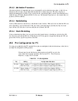
29.4.2 Arbitration Procedure
The relative priority of competing devices is determined by a data arbitration procedure. A device loses
arbitration when it sends a logic high while another device sends a logic low. The device that loses
arbitration immediately switches to slave-receive mode, stops driving SDA, and sets the Arbitration Lost
(IAL) bit in its I
2
C Status Register (I2SR). In this case, the transition from master to slave mode does not
generate a STOP condition.
29.4.3 Handshaking
Clock synchronization can function as a handshake in data transfers. When slave devices hold the SCL low
after completing a one byte transfer (9 bits), the clock synchronization feature halts the bus clock and
forces the master clock into a wait state until the slave releases the SCL.
29.4.4 Clock Stretching
Clock synchronization allows slaves to slow down the transfer bit rate. After the master drives the SCL
low, the slave can hold the SCL low. When the slave SCL low period is longer than the master SCL low
period, the SCL bus signal low period is stretched.
29.5 Pin Configuration for I
2
C
Two pins are available for the I
2
C module. These pins are multiplexed with other functions on the device
and must be configured for SPI operation.
NOTE:
The user must ensure that the data direction bits in the GPIO are set to the
correct direction for proper operation. See Section 32.5.1, “Data Direction
Registers,” on page 32-9 for details.
Table 29-1. Pin Configuration
Pin
Setting
Configuration Procedure
I2C_SCL
Primary function of
GPIO Port A [16]
1. Clear bit 16 of Port A GPIO In Use Register (GIUS_A)
2. Clear bit 16 of Port A General Purpose Register (GPR_A)
I2C_SDA
Primary function of
GPIO Port A [15]
1. Clear bit 15 of Port A GPIO In Use Register (GIUS_A)
2. Clear bit 15 of Port A General Purpose Register (GPR_A)
Summary of Contents for DragonBall MC9328MX1
Page 68: ...1 12 MC9328MX1 Reference Manual MOTOROLA Introduction ...
Page 86: ...2 18 MC9328MX1 Reference Manual MOTOROLA Signal Descriptions and Pin Assignments ...
Page 116: ...3 30 MC9328MX1 Reference Manual MOTOROLA Memory Map ...
Page 126: ...4 10 MC9328MX1 Reference Manual MOTOROLA ARM920T Processor ...
Page 160: ...8 8 MC9328MX1 Reference Manual MOTOROLA System Control ...
Page 272: ...13 32 MC9328MX1 Reference Manual MOTOROLA DMA Controller ...
Page 281: ...Programming Model MOTOROLA Watchdog Timer Module 14 9 ...
Page 282: ...14 10 MC9328MX1 Reference Manual MOTOROLA Watchdog Timer Module ...
Page 300: ...15 18 MC9328MX1 Reference Manual MOTOROLA Analog Signal Processor ASP ...
Page 438: ...18 16 MC9328MX1 Reference Manual MOTOROLA Serial Peripheral Interface Modules SPI 1 and SPI 2 ...
Page 478: ...19 40 MC9328MX1 Reference Manual MOTOROLA LCD Controller ...
Page 574: ...21 32 MC9328MX1 Reference Manual MOTOROLA Memory Stick Host Controller MSHC Module ...
Page 598: ...23 16 MC9328MX1 Reference Manual MOTOROLA Real Time Clock RTC ...
Page 670: ...24 72 MC9328MX1 Reference Manual MOTOROLA SDRAM Memory Controller ...
Page 726: ...25 56 MC9328MX1 Reference Manual MOTOROLA SmartCard Interface Module SIM ...
Page 736: ...26 10 MC9328MX1 Reference Manual MOTOROLA General Purpose Timers ...
Page 854: ...29 18 MC9328MX1 Reference Manual MOTOROLA I2C Module ...
Page 900: ...30 46 MC9328MX1 Reference Manual MOTOROLA Synchronous Serial Interface SSI ...
Page 942: ...32 26 MC9328MX1 Reference Manual MOTOROLA GPIO Module and I O Multiplexer IOMUX ...


