27-32
MC9328MX1 Reference Manual
MOTOROLA
Universal Asynchronous Receiver/Transmitters (UART) Modules
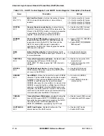
AWAKEN
Bit 4
Asynchronous WAKE Interrupt Enable
—Controls
the asynchronous WAKE interrupt. An interrupt is
generated when AWAKEN is asserted and a falling
edge is detected on the RXD pin.
0 = Disable the AWAKE interrupt
1 = Enable the AWAKE interrupt
REF25
Bit 3
Reference Frequency 25 MHz
—Indicates to the
hardware that a reference clock frequency of 25 MHz
is used. The reference clock is derived from the input
clock IPG_CLK via the programmable divider.
0 = 25 MHz reference clock not used
1 = 25 MHz reference clock used
REF30
Bit 2
Reference Frequency 30 Mhz
—Indicates to the
hardware that a reference clock frequency of 30 MHz
is used. The reference clock is derived from the input
clock IPG_CLK via the programmable divider.
0 = 30 MHz reference clock not used
1 = 30 MHz reference clock used
INVT
Bit 1
Inverted Infrared Transmission
—Sets the active
level for the transmission. When INVT is cleared, the
infrared logic block transmits a positive IR 3/16 pulse
for all 0s and 0s are transmitted for 1s. When INVT is
set (INVT
=
1), the infrared logic block transmits an
active low or negative infrared 3/16 pulse for all 0s
and 1s are transmitted for 1s.
0 = Active low transmission
1 = Active high transmission
BPEN
Bit 0
Preset Registers Enable
—Activates the BRM
preset registers for use during automatic baud rate
detection mode. When BPEN is deasserted, the
remainder from the automatic baud count register
divided by 16 is ignored. When BPEN is asserted,
the remainder and the dividend chooses the
appropriate preset register on the detection of special
baud rates. If the criteria is not met for selecting one
of the preset registers, integer division is performed
by writing one less than the dividend to the
UBMR_1/UBMR_2 register.
0 = The BRM preset registers are not used
(normal operation)
1 = The BRM preset registers are used
(auto detect special baud rates)
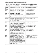
Table 27-16. UART1 Control Register 3 Description (Continued)
Name
Description
Settings
Summary of Contents for DragonBall MC9328MX1
Page 68: ...1 12 MC9328MX1 Reference Manual MOTOROLA Introduction ...
Page 86: ...2 18 MC9328MX1 Reference Manual MOTOROLA Signal Descriptions and Pin Assignments ...
Page 116: ...3 30 MC9328MX1 Reference Manual MOTOROLA Memory Map ...
Page 126: ...4 10 MC9328MX1 Reference Manual MOTOROLA ARM920T Processor ...
Page 160: ...8 8 MC9328MX1 Reference Manual MOTOROLA System Control ...
Page 272: ...13 32 MC9328MX1 Reference Manual MOTOROLA DMA Controller ...
Page 281: ...Programming Model MOTOROLA Watchdog Timer Module 14 9 ...
Page 282: ...14 10 MC9328MX1 Reference Manual MOTOROLA Watchdog Timer Module ...
Page 300: ...15 18 MC9328MX1 Reference Manual MOTOROLA Analog Signal Processor ASP ...
Page 438: ...18 16 MC9328MX1 Reference Manual MOTOROLA Serial Peripheral Interface Modules SPI 1 and SPI 2 ...
Page 478: ...19 40 MC9328MX1 Reference Manual MOTOROLA LCD Controller ...
Page 574: ...21 32 MC9328MX1 Reference Manual MOTOROLA Memory Stick Host Controller MSHC Module ...
Page 598: ...23 16 MC9328MX1 Reference Manual MOTOROLA Real Time Clock RTC ...
Page 670: ...24 72 MC9328MX1 Reference Manual MOTOROLA SDRAM Memory Controller ...
Page 726: ...25 56 MC9328MX1 Reference Manual MOTOROLA SmartCard Interface Module SIM ...
Page 736: ...26 10 MC9328MX1 Reference Manual MOTOROLA General Purpose Timers ...
Page 854: ...29 18 MC9328MX1 Reference Manual MOTOROLA I2C Module ...
Page 900: ...30 46 MC9328MX1 Reference Manual MOTOROLA Synchronous Serial Interface SSI ...
Page 942: ...32 26 MC9328MX1 Reference Manual MOTOROLA GPIO Module and I O Multiplexer IOMUX ...


