11-16
MC9328MX1 Reference Manual
MOTOROLA
External Interface Module (EIM)
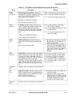
EDC
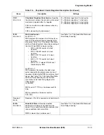
Bits 35–32
Extra Dead Cycles
—Determines whether idle
cycles are inserted after a read cycle for
back-to-back external transfers to eliminate data
bus contention. This is useful for slow memory
and peripherals that use long CS or OE to output
data three-state times. Idle cycles are not inserted
for back-to-back external reads from the same
chip select.
EDC is cleared by a hardware reset.
0000 = 0 Idle cycles inserted
0001 = 1 Idle cycle inserted
...
1111 = 15 Idle cycles inserted
OEA
Bits 31–28
OE Assert
—Determines when OE is asserted
during read cycles.
For SYNC = 0:
OEA determines the number of half clocks before
OE asserts during a read cycle.
For SYNC = 1:
After the initial burst access, OE is asserted
continuously for subsequent burst accesses, and
is not affected by OEA (see burst read timing
diagrams for more detail). The behavior of OE on
the initial burst access is the same as when
SYNC = 0.
When the EBC bit in the corresponding register is
clear, the EB [3:0] outputs are similarly affected.
The OEA bits do not affect the cycle length.
OEA is cleared by a hardware reset.
0000 = 0 half clocks before assertion
0001 = 1 half clock before assertion
...
1111 = 15 half clocks before assertion
OEN
Bits 27–24
OE Negate
—Determines when OE is negated
during a read cycle. Setting the SYNC bit (SYNC
= 1) overrides OEN and OE negates at the end of
a read access and no sooner. When EBC in the
corresponding register is clear, the EB [3:0]
outputs are similarly affected.
OEN does not affect the cycle length.
OEN is cleared by a hardware reset.
0000 = 0 half clocks before end of access
0001 = 1 half clock before end of access
...
1111 = 15 half clocks before end of access
WEA
Bits 23–20
EB [3:0] Assert
—Determines when EB [3:0] is
asserted during write cycles. This is useful to
meet data setup time requirements for slow
memories.
WEA does not affect the cycle length.
WEA is cleared by a hardware reset.
0000 = 0 half clocks before assertion
0001 = 1 half clock before assertion
...
1111 = 15 half clocks before assertion
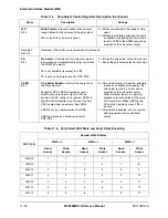
Table 11-5. Chip Select Control Registers Description (Continued)
Name
Description
Settings
Summary of Contents for DragonBall MC9328MX1
Page 68: ...1 12 MC9328MX1 Reference Manual MOTOROLA Introduction ...
Page 86: ...2 18 MC9328MX1 Reference Manual MOTOROLA Signal Descriptions and Pin Assignments ...
Page 116: ...3 30 MC9328MX1 Reference Manual MOTOROLA Memory Map ...
Page 126: ...4 10 MC9328MX1 Reference Manual MOTOROLA ARM920T Processor ...
Page 160: ...8 8 MC9328MX1 Reference Manual MOTOROLA System Control ...
Page 272: ...13 32 MC9328MX1 Reference Manual MOTOROLA DMA Controller ...
Page 281: ...Programming Model MOTOROLA Watchdog Timer Module 14 9 ...
Page 282: ...14 10 MC9328MX1 Reference Manual MOTOROLA Watchdog Timer Module ...
Page 300: ...15 18 MC9328MX1 Reference Manual MOTOROLA Analog Signal Processor ASP ...
Page 438: ...18 16 MC9328MX1 Reference Manual MOTOROLA Serial Peripheral Interface Modules SPI 1 and SPI 2 ...
Page 478: ...19 40 MC9328MX1 Reference Manual MOTOROLA LCD Controller ...
Page 574: ...21 32 MC9328MX1 Reference Manual MOTOROLA Memory Stick Host Controller MSHC Module ...
Page 598: ...23 16 MC9328MX1 Reference Manual MOTOROLA Real Time Clock RTC ...
Page 670: ...24 72 MC9328MX1 Reference Manual MOTOROLA SDRAM Memory Controller ...
Page 726: ...25 56 MC9328MX1 Reference Manual MOTOROLA SmartCard Interface Module SIM ...
Page 736: ...26 10 MC9328MX1 Reference Manual MOTOROLA General Purpose Timers ...
Page 854: ...29 18 MC9328MX1 Reference Manual MOTOROLA I2C Module ...
Page 900: ...30 46 MC9328MX1 Reference Manual MOTOROLA Synchronous Serial Interface SSI ...
Page 942: ...32 26 MC9328MX1 Reference Manual MOTOROLA GPIO Module and I O Multiplexer IOMUX ...


