Programming Model
MOTOROLA
LCD Controller
19-23
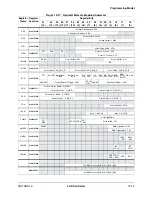
FLMPOL
Bit 23
First Line Marker Polarity
—Sets the polarity of
the first line marker symbol.
0 = Active high
1 = Active low
LPPOL
Bit 22
Line Pulse Polarity
—Sets the polarity of the line
pulse signal.
0 = Active high
1 = Active low
CLKPOL
Bit 21
LCD Shift Clock Polarity
—Sets the polarity of
the active edge of the LCD shift clock.
0 = Active negative edge of LSCLK (in TFT
mode, active on positive edge of LSCLK)
1 = Active positive edge of LSCLK (in TFT
mode, active on negative edge of LSCLK)
OEPOL
Bit 20
Output Enable Polarity
—Sets the polarity of the
output enable signal.
0 = Active high
1 = Active low
SCLKIDLE
Bit 19
LSCLK Idle Enable
—Enables/Disables LSCLK
when VSYNC is idle in TFT mode.
0 = Disable LSCLK
1 = Enable LSCLK
END_SEL
Bit 18
Endian Select
—Selects the image download into
memory as big or little endian format.
0 = Little endian
1 = Big endian
SWAP_SEL
Bit 17
Swap Select
—Controls the swap of data in little
endian mode (when END_SEL = 1 this bit has no
effect).
0 = 16 bpp mode
1 = 8 bpp. 4 bpp, 2 bpp, 1 bpp mode
REV_VS
Bit 16
Reverse Vertical Scan
—Selects the vertical
scan direction as normal or reverse (the image
flips along the x-axis). The SSA register must be
changed accordingly.
0 = Vertical scan in normal direction
1 = Vertical scan in reverse direction
ACDSEL
Bit 15
ACD Clock Source Select
—Selects the clock
source used by the alternative crystal direction
counter.
0 = Use FRM as clock source for ACD count
1 = Use LP/HSYN as clock source for ACD
count
ACD
Bits 14–8
Alternate Crystal Direction
—Toggles the ACD
signal once every 1-16 FLM cycles based on the
value specified in this field. The actual number of
FLM cycles between toggles is the programmed
value plus one.
For active mode (TFT=1), this parameter is not
used.
For passive mode (TFT=0), see description.
SCLKSEL
Bit 7
LSCLK Select
—Selects whether to enable or
disable LSCLK in TFT mode when there is no
data output.
0 = Disable OE and LSCLK in TFT mode when
no data output
1 = Always enable LSCLK in TFT mode even if
there is no data output
SHARP
Bit 6
Sharp Panel Enable
—Enables/Disables signals
for Sharp HR-TFT 320 x 240 panels.
0 = Disable Sharp signals
1 = Enable Sharp signals
PCD
Bits 5–0
Pixel Clock Divider
—Holds clock divider value.
The LCDC_CLK (PerCLK2) is divided by N (PCD
plus one) to yield the pixel clock rate. Values of 1
to 63 will yield N=2 to 64. The pixel clock rate is
faster than LSCLK by a factor equal to the
number of pixels in an output vector.
For passive matrix color panels (COLOR=1,
TFT=0, PBSIZ=11) PCD must be greater than or
equal to 2.
The value of PCD must be set such that the
LSCLK frequency is less than or equal to one
fifth of the HCLK frequency, otherwise the LD
will be wrong.
When PCD = O, pixel clock frequency is equal
to LCDC_CLK frequency.
Table 19-12. Panel Configuration Register Description (Continued)
Name
Description
Settings
Summary of Contents for DragonBall MC9328MX1
Page 68: ...1 12 MC9328MX1 Reference Manual MOTOROLA Introduction ...
Page 86: ...2 18 MC9328MX1 Reference Manual MOTOROLA Signal Descriptions and Pin Assignments ...
Page 116: ...3 30 MC9328MX1 Reference Manual MOTOROLA Memory Map ...
Page 126: ...4 10 MC9328MX1 Reference Manual MOTOROLA ARM920T Processor ...
Page 160: ...8 8 MC9328MX1 Reference Manual MOTOROLA System Control ...
Page 272: ...13 32 MC9328MX1 Reference Manual MOTOROLA DMA Controller ...
Page 281: ...Programming Model MOTOROLA Watchdog Timer Module 14 9 ...
Page 282: ...14 10 MC9328MX1 Reference Manual MOTOROLA Watchdog Timer Module ...
Page 300: ...15 18 MC9328MX1 Reference Manual MOTOROLA Analog Signal Processor ASP ...
Page 438: ...18 16 MC9328MX1 Reference Manual MOTOROLA Serial Peripheral Interface Modules SPI 1 and SPI 2 ...
Page 478: ...19 40 MC9328MX1 Reference Manual MOTOROLA LCD Controller ...
Page 574: ...21 32 MC9328MX1 Reference Manual MOTOROLA Memory Stick Host Controller MSHC Module ...
Page 598: ...23 16 MC9328MX1 Reference Manual MOTOROLA Real Time Clock RTC ...
Page 670: ...24 72 MC9328MX1 Reference Manual MOTOROLA SDRAM Memory Controller ...
Page 726: ...25 56 MC9328MX1 Reference Manual MOTOROLA SmartCard Interface Module SIM ...
Page 736: ...26 10 MC9328MX1 Reference Manual MOTOROLA General Purpose Timers ...
Page 854: ...29 18 MC9328MX1 Reference Manual MOTOROLA I2C Module ...
Page 900: ...30 46 MC9328MX1 Reference Manual MOTOROLA Synchronous Serial Interface SSI ...
Page 942: ...32 26 MC9328MX1 Reference Manual MOTOROLA GPIO Module and I O Multiplexer IOMUX ...


