21-24
MC9328MX1 Reference Manual
MOTOROLA
Memory Stick Host Controller (MSHC) Module
21.8 Programmer’s Reference
21.8.1 Memory Stick Serial Interface Overview
The Memory Stick Protocol requires 3 interface signal line connections for data transfers: MS_BS,
MS_SDIO, and MS_SCLKO (or MS_SCLKI). MS_PI [1:0] pin inputs detect insertion/removal of
Memory Stick. Communication is always started from the MSHC module and operates the bus in either
Four State Access or Two State Access mode.
MS_BS classifies data on SDIO into one of four states (BS0, BS1, BS2 or BS3) according to the attribute
and transfer direction. BS0 state has no packet communication going on while three states (BS1, BS2, and
BS3) have packet communication being executed. BS1 through BS3 are regarded as one packet and one
communication transfer is always completed within one packet (in Four State Access Mode).
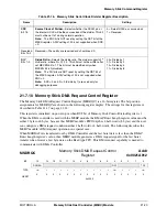
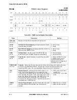
Table 21-17. Memory Stick DMA Request Control Register Description
Name
Description
Setting
DRQEN
Bit 15
DMA Request Enable
—Enables/Disables operation of the
DMA request signal.
Note:
This bit must be set to 1 before initiating DMA
transfer.
0 = Disable DMA transfer requests
1 = Enable DMA transfer requests
Reserved
Bits 14–5
Reserved—These bits are reserved and should read 0.
RFF
Bit 4
Rx FIFO Full DMA Request
—Controls the DMA request
signal in case PID/APID is a read command.
Note:
This bit is effective only in case of DAKEN bit of
MSCS register is 1. When DAKEN is 0, MSHC module
generates DMA request in condition of RFF = 0. Therefore,
when user need to use in condition of RFF = 1, DAKEN bit
must be set to 1.
0 = Generate DMA request when
Rx FIFO has received at least
one half-word (use for DMA
transfer of 1 half-word (16 bits))
1 = Generate DMA request when
Rx FIFO is full (4 half-words)
Reserved
Bits 3–1
Reserved—These bits are reserved and should read 0.
TFE
Bit 0
Tx FIFO Empty DMA Request
—Controls the DMA request
signal in case of PID is a write command.
Note:
This bit is effective only in case of DAKEN bit of
MSCS register is 1. When DAKEN is 0, MSHC module
generates DMA request in condition of TFE = 0. Therefore,
when user need to use in condition of TFE = 1, DAKEN bit
must be set to 1.
0 = Generate DMA request when at
least 1 empty slot is available in
Tx FIFO (use for DMA transfer
of 1 half-word (16 bits))
1 = Generate DMA request when
Tx FIFO is empty
Summary of Contents for DragonBall MC9328MX1
Page 68: ...1 12 MC9328MX1 Reference Manual MOTOROLA Introduction ...
Page 86: ...2 18 MC9328MX1 Reference Manual MOTOROLA Signal Descriptions and Pin Assignments ...
Page 116: ...3 30 MC9328MX1 Reference Manual MOTOROLA Memory Map ...
Page 126: ...4 10 MC9328MX1 Reference Manual MOTOROLA ARM920T Processor ...
Page 160: ...8 8 MC9328MX1 Reference Manual MOTOROLA System Control ...
Page 272: ...13 32 MC9328MX1 Reference Manual MOTOROLA DMA Controller ...
Page 281: ...Programming Model MOTOROLA Watchdog Timer Module 14 9 ...
Page 282: ...14 10 MC9328MX1 Reference Manual MOTOROLA Watchdog Timer Module ...
Page 300: ...15 18 MC9328MX1 Reference Manual MOTOROLA Analog Signal Processor ASP ...
Page 438: ...18 16 MC9328MX1 Reference Manual MOTOROLA Serial Peripheral Interface Modules SPI 1 and SPI 2 ...
Page 478: ...19 40 MC9328MX1 Reference Manual MOTOROLA LCD Controller ...
Page 574: ...21 32 MC9328MX1 Reference Manual MOTOROLA Memory Stick Host Controller MSHC Module ...
Page 598: ...23 16 MC9328MX1 Reference Manual MOTOROLA Real Time Clock RTC ...
Page 670: ...24 72 MC9328MX1 Reference Manual MOTOROLA SDRAM Memory Controller ...
Page 726: ...25 56 MC9328MX1 Reference Manual MOTOROLA SmartCard Interface Module SIM ...
Page 736: ...26 10 MC9328MX1 Reference Manual MOTOROLA General Purpose Timers ...
Page 854: ...29 18 MC9328MX1 Reference Manual MOTOROLA I2C Module ...
Page 900: ...30 46 MC9328MX1 Reference Manual MOTOROLA Synchronous Serial Interface SSI ...
Page 942: ...32 26 MC9328MX1 Reference Manual MOTOROLA GPIO Module and I O Multiplexer IOMUX ...

