Programming Model
MOTOROLA
SDRAM Memory Controller
24-9
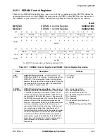
24.5.1 SDRAM Control Registers
There are two SDRAM Control Registers, one for each of the two memory regions. SDCTL0 defines the
operating characteristics for the SDRAM 0 region (selected by CSD0), while SDCTL1 does the same for
the SDRAM 1 region (selected by CSD1). Bit and field assignments within the registers are identical.
SDCTL0
SDCTL1
SDRAM 0 Control Register
SDRAM 1 Control Register
Addr
0x00221000
0x00221004
BIT
31
30
29
28
27
26
25
24
23
22
21
20
19
18
17
16
SDE
SMODE
SP
ROW
COL
IAM
DSIZ
TYPE
rw
rw
rw
rw
rw
r
rw
rw
r
r
rw
rw
rw
r
rw
rw
RESET
0*
0
0
0
0
0
0
1
0
0
0
0
0
0
0*
0*
0x0100*
BIT
15
14
13
12
11
10
9
8
7
6
5
4
3
2
1
0
SREFR
CLKST
SCL
SRP
SRCD
SRC
TYPE
rw
rw
rw
rw
r
r
rw
rw
r
rw
rw
rw
r
rw
rw
rw
RESET
0
0
0
0
0
0
1
1
0
0
0
0
0
0
0
0
0x0300
* For
SDCTL1, the reset state is affected by bootmod [1:0]
Table 24-7. SDRAM 0 Control Register and SDRAM 1 Control Register Description
Name
Description
Settings
SDE
Bit 31
SDRAM Controller Enable
—Enables/Disables the
SDRAM controller. The module is disabled on reset. For
SDRAM 1, if the selected boot mode is the SyncFlash
memory, the module will be enabled on reset. Disabling
the module shuts off all clocks within the module with
the exception of register accesses.
0 = Disabled
1 = Enabled
SMODE
Bits 30–28
SDRAM Controller Operating Mode
—Determines the
operating mode of the SDRAM controller. The controller
is capable of operating in six different modes. These
modes are primarily used for SDRAM initialization and
programming of the SyncFlash memory. Any access to
the SDRAM memory space, while in one of the alternate
modes, will result in the corresponding special cycle
being run. Moving from Normal to any other mode does
not close (precharge) any banks that may be open
(activated). Under most circumstances, software must
run a precharge-all cycle when transitioning out of
Normal Read/Write mode. SyncFlash command register
read/write sequences are the one exception that does
not require a software initiated precharge. Operating
mode details are provided in Section 24.8, “SDRAM
Operation,” and Section 24.9, “SyncFlash Operation.”
Reset initializes the operating mode to “Normal
Read/Write”.
000 = Normal Read/Write
001 = Precharge Command
010 = Auto-Refresh Command
011 = Set Mode Register Command
100 = Reserved
101 = Reserved
110 = SyncFlash Load Command
Register
111 = SyncFlash Program Read/Write
Summary of Contents for DragonBall MC9328MX1
Page 68: ...1 12 MC9328MX1 Reference Manual MOTOROLA Introduction ...
Page 86: ...2 18 MC9328MX1 Reference Manual MOTOROLA Signal Descriptions and Pin Assignments ...
Page 116: ...3 30 MC9328MX1 Reference Manual MOTOROLA Memory Map ...
Page 126: ...4 10 MC9328MX1 Reference Manual MOTOROLA ARM920T Processor ...
Page 160: ...8 8 MC9328MX1 Reference Manual MOTOROLA System Control ...
Page 272: ...13 32 MC9328MX1 Reference Manual MOTOROLA DMA Controller ...
Page 281: ...Programming Model MOTOROLA Watchdog Timer Module 14 9 ...
Page 282: ...14 10 MC9328MX1 Reference Manual MOTOROLA Watchdog Timer Module ...
Page 300: ...15 18 MC9328MX1 Reference Manual MOTOROLA Analog Signal Processor ASP ...
Page 438: ...18 16 MC9328MX1 Reference Manual MOTOROLA Serial Peripheral Interface Modules SPI 1 and SPI 2 ...
Page 478: ...19 40 MC9328MX1 Reference Manual MOTOROLA LCD Controller ...
Page 574: ...21 32 MC9328MX1 Reference Manual MOTOROLA Memory Stick Host Controller MSHC Module ...
Page 598: ...23 16 MC9328MX1 Reference Manual MOTOROLA Real Time Clock RTC ...
Page 670: ...24 72 MC9328MX1 Reference Manual MOTOROLA SDRAM Memory Controller ...
Page 726: ...25 56 MC9328MX1 Reference Manual MOTOROLA SmartCard Interface Module SIM ...
Page 736: ...26 10 MC9328MX1 Reference Manual MOTOROLA General Purpose Timers ...
Page 854: ...29 18 MC9328MX1 Reference Manual MOTOROLA I2C Module ...
Page 900: ...30 46 MC9328MX1 Reference Manual MOTOROLA Synchronous Serial Interface SSI ...
Page 942: ...32 26 MC9328MX1 Reference Manual MOTOROLA GPIO Module and I O Multiplexer IOMUX ...


