Operating Modes
MOTOROLA
SDRAM Memory Controller
24-19
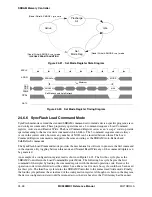
Read/write cycles, refresh and low-power mode requests, and clock suspend time-outs will all trigger
transitions out of the idle state. State transitions due to a read or write request depend on the operating
mode. Other transitions require the corresponding function to be enabled in the SDCTL register. Some
state transitions have been removed to minimize complexity and allow an easier understanding of the basic
controller operation.
The following subsections document the operation of each of the operating modes.
24.6.2 Normal Read/Write Mode (SMODE = 000)
The Normal Read/Write mode (SMODE = 000) is used for general read and write access to the SDRAM
controller, and for reads of the SyncFlash. SyncFlash writes use the SyncFlash Program mode (See
Section 24.6.7, “SyncFlash Program Mode.” ) Both single and burst accesses are supported, although burst
requests are limited to a length of 8 words (one word = 32 bits).
Read or write requests to the SDRAM Controller initiate a check to see whether the page is already open.
This check consists of comparing the request address against the last row accessed within the
corresponding bank. If the rows are different, it indicates that a precharge has occurred after the last access,
or there has never been an access to the bank. In that case, the access must follow the “off-page” sequence.
If the requested row and last row match, the shorter “on-page” access is used.
An off-page sequence must first activate the requested row, an operation which is analogous to a
conventional DRAM RAS cycle. An activate cycle is the first operation depicted in Figure 24-7. During
the activate cycle, the appropriate chip-select is driven low, the row addresses are placed on the
multiplexed address pins, the non-multiplexed addresses are driven to their respective values, write enable
is driven high, CAS is driven high, and RAS is driven low. These latter three pins form the SDRAM
command word. The data bus is unused during the activate command.
When the selected row has been activated, the read operation begins after the row-to-column delay (t
RCD
)
has been met. This delay is either 2 or 3 clocks, as determined by the SRCD field of the appropriate control
register. During the read cycle, the chip-select is once again asserted, the column addresses are driven onto
the multiplexed address bus, the non-multiplexed addresses remain driven to the value presented during
the activate cycle, the write enable is driven high, RAS is driven high, and CAS is driven low. After the
CAS latency has expired, data is transferred across the data bus. CAS latency is programmable via the SCL
field of the control register. As data is being returned across the AHB, transfer acknowledge is asserted
back to the CPU indicating that the CPU must latch data. While data is still on the bus, the SDRAM
Controller must begin monitoring transfer requests because the CPU is free to issue the next bus request on
the same edge that data is being latched.
Data transfers can be either single operand or a burst of up to 8 operands. Burst requests are designated as
such by the P_BURST attribute. It is activated by the load multiple command from the ARM920T core
when the data or instruction cache is enabled. This AHB signal is asserted low for all except the last
operand of a burst transfer. Non-burst transfers do not assert the signal.
SDRAM memories assume that all transfers are burst transfers unless terminated early. Burst transfers can
be terminated by a variety of mechanisms: another read or write cycle, a precharge operation, or a burst
terminate command. Burst terminate commands are the general mechanism used by the SDRAM
controller for early burst termination. The burst terminate command is subject to the CAS latency and must
be pipelined similar to the Read command, as shown in Figure 25-7 and Figure 25-8. When a load-multiple
command is executed, the SDRAM controller will not issue a burst terminate command.
SDRAM write cycles are different than read cycles in one important aspect. Whereas read data was
delayed by the CAS latency, write data has no delay and is supplied at the same time as the Write
command. Figure 25-13 illustrates an off-page write cycle followed by an on-page write cycle. Note that
the write data is driven during the same clock that the Write command is issued. The SDRAM controller
only supports single burst writes and does not issue a burst terminate after each write. Therefore, the user
Summary of Contents for DragonBall MC9328MX1
Page 68: ...1 12 MC9328MX1 Reference Manual MOTOROLA Introduction ...
Page 86: ...2 18 MC9328MX1 Reference Manual MOTOROLA Signal Descriptions and Pin Assignments ...
Page 116: ...3 30 MC9328MX1 Reference Manual MOTOROLA Memory Map ...
Page 126: ...4 10 MC9328MX1 Reference Manual MOTOROLA ARM920T Processor ...
Page 160: ...8 8 MC9328MX1 Reference Manual MOTOROLA System Control ...
Page 272: ...13 32 MC9328MX1 Reference Manual MOTOROLA DMA Controller ...
Page 281: ...Programming Model MOTOROLA Watchdog Timer Module 14 9 ...
Page 282: ...14 10 MC9328MX1 Reference Manual MOTOROLA Watchdog Timer Module ...
Page 300: ...15 18 MC9328MX1 Reference Manual MOTOROLA Analog Signal Processor ASP ...
Page 438: ...18 16 MC9328MX1 Reference Manual MOTOROLA Serial Peripheral Interface Modules SPI 1 and SPI 2 ...
Page 478: ...19 40 MC9328MX1 Reference Manual MOTOROLA LCD Controller ...
Page 574: ...21 32 MC9328MX1 Reference Manual MOTOROLA Memory Stick Host Controller MSHC Module ...
Page 598: ...23 16 MC9328MX1 Reference Manual MOTOROLA Real Time Clock RTC ...
Page 670: ...24 72 MC9328MX1 Reference Manual MOTOROLA SDRAM Memory Controller ...
Page 726: ...25 56 MC9328MX1 Reference Manual MOTOROLA SmartCard Interface Module SIM ...
Page 736: ...26 10 MC9328MX1 Reference Manual MOTOROLA General Purpose Timers ...
Page 854: ...29 18 MC9328MX1 Reference Manual MOTOROLA I2C Module ...
Page 900: ...30 46 MC9328MX1 Reference Manual MOTOROLA Synchronous Serial Interface SSI ...
Page 942: ...32 26 MC9328MX1 Reference Manual MOTOROLA GPIO Module and I O Multiplexer IOMUX ...


