background image

Programming Model

MOTOROLA

Bluetooth Accelerator (BTA)

16-65

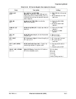
16.5.8   Wake-Up Registers

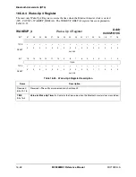
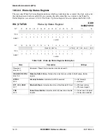
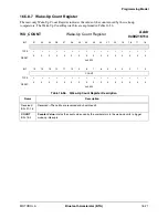
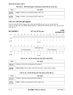
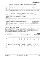
Five addresses pertain to wake-up functions. The WakeUp Control Register and Wake-Up Status Register 
are write and read registers associated with one address.

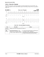
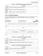
16.5.8.1   Wake-Up 1 Register

The Wake-Up 1 Register contains the comparator value that determines the time for the power-down 
event. 

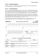
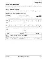
The Wake-Up 1 Register bits are explained in Table 16-50.

WAKEUP_1

Wake-Up 1 Register

Addr

0x00216100

BIT

31

30

29

28

27

26

25

24

23

22

21

20

19

18

17

16

TYPE

r

r

r

r

r

r

r

r

r

r

r

r

r

r

r

r

RESET

0

0

0

0

0

0

0

0

0

0

0

0

0

0

0

0

0x0000

BIT

15

14

13

12

11

10

9

8

7

6

5

4

3

2

1

0

TIME

TYPE

r

r

r

r

r

r

r

r

r

r

r

r

r

r

rw

rw

RESET

0

0

0

0

0

0

0

0

0

0

0

0

0

0

0

1

0x0001

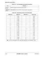
Table 16-50.   Wake-Up 1 Register Description

Name

Description

Settings

Reserved
Bits 31–2

Reserved—These bits are reserved and should read 0.

TIME

Bits 1–0

Value for Wake-Up Timer 1

—Sets wake-up timer 1 for low-power 

operation. The timer is clocked by the 32 kHz clock.

Recommend using 
values greater than 1.

Summary of Contents for DragonBall MC9328MX1

Page 1: ...MC9328MX1RM D Rev 2 02 2003 DragonBall MC9328MX1 Integrated Portable System Processor Reference Manual ...

Page 2: ...ers including Typicals must be validated for each customer application by customer s technical experts Motorola does not convey any license under its patent rights nor the rights of others Motorola products are not designed intended or authorized for use as components in systems intended for surgical implant into the body or other applications intended to support or sustain life or for any other a...

Page 3: ... Two General Purpose 32 Bit Counters Timers 1 5 1 11 Watchdog Timer 1 5 1 12 Real Time Clock Sampling Timer RTC 1 6 1 13 LCD Controller LCDC 1 6 1 14 Pulse Width Modulation PWM Module 1 6 1 15 Universal Serial Bus USB Device 1 7 1 16 Multimedia Card and Secure Digital MMC SD Host Controller 1 7 1 17 Memory Stick Host Controller MSHC 1 8 1 18 SmartCard Interface Module SIM 1 8 1 19 Direct Memory Ac...

Page 4: ...ARM920T Macrocell 4 2 4 2 1 Caches 4 2 4 2 2 Cache Lock Down 4 3 4 2 3 Write Buffer 4 3 4 2 4 PATAG RAM 4 3 4 2 5 MMUs 4 3 4 2 6 System Controller 4 3 4 2 7 Control Coprocessor CP15 4 4 4 3 ARMv4T Architecture 4 4 4 3 1 Registers 4 4 4 3 2 Modes and Exception Handling 4 4 4 3 3 Status Registers 4 4 4 3 4 Exception Types 4 5 4 3 5 Conditional Execution 4 5 4 4 Four Classes of Instructions 4 5 4 4 1...

Page 5: ...rs 1 0 7 12 7 2 1 1 AIPI1 Peripheral Size Register 0 and AIPI2 Peripheral Size Register 0 7 12 7 2 1 2 AIPI1 Peripheral Size Register 1 and AIPI2 Peripheral Size Register 1 7 13 7 2 2 Peripheral Access Registers 7 14 7 2 3 Peripheral Control Register 7 15 7 2 4 Time Out Status Register 7 16 7 3 Programming Example 7 17 7 3 1 Data Access to 8 Bit Peripherals 7 17 7 3 2 Data Access to 16 Bit Periphe...

Page 6: ...nable Register Low 10 13 10 4 6 Interrupt Type Register High and Interrupt Type Register Low 10 14 10 4 6 1 Interrupt Type Register High 10 14 10 4 6 2 Interrupt Type Register Low 10 15 10 4 7 Normal Interrupt Priority Level Registers 10 15 10 4 7 1 Normal Interrupt Priority Level Register 7 10 16 10 4 7 2 Normal Interrupt Priority Level Register 6 10 17 10 4 7 3 Normal Interrupt Priority Level Re...

Page 7: ...rrupt Routines 10 36 Chapter 11 External Interface Module EIM 11 1 Overview 11 1 11 2 EIM I O Signals 11 1 11 2 1 Address Bus 11 1 11 2 2 Data Bus 11 1 11 2 3 Read Write 11 2 11 2 4 Control Signals 11 2 11 2 4 1 OE Output Enable 11 2 11 2 4 2 EB 3 0 Enable Bytes 11 2 11 2 4 3 DTACK Data Transfer Acknowledge 11 2 11 2 5 Chip Select Outputs 11 2 11 2 5 1 Chip Select 0 CS0 11 2 11 2 5 2 Chip Select 1...

Page 8: ...t in the Clock Controller 12 4 12 5 Programming Model 12 5 12 5 1 Clock Source Control Register 12 5 12 5 2 Peripheral Clock Divider Register 12 8 12 5 3 Programming Digital Phase Locked Loops 12 9 12 5 3 1 MCU PLL Control Register 0 12 9 12 5 3 2 MCU PLL and System Clock Control Register 1 12 11 12 5 4 Generation of 48 MHz Clocks 12 11 12 5 4 1 System PLL Control Register 0 12 12 12 5 4 2 System ...

Page 9: ...mer Module 14 1 General Overview 14 1 14 2 Watchdog Timer Operation 14 1 14 2 1 Timing Specifications 14 1 14 2 2 Watchdog During Reset 14 2 14 2 2 1 Power On Reset 14 2 14 2 2 2 Software Reset 14 2 14 3 Watchdog After Reset 14 2 14 3 1 Initial Load 14 2 14 3 2 Countdown 14 2 14 3 3 Reload 14 2 14 3 4 Time Out 14 3 14 3 5 Halting the Counter 14 3 14 4 Watchdog Control 14 3 14 4 1 Interrupt Control...

Page 10: ...3 1 Bluetooth Core 16 3 16 3 1 1 IP Bus Interface 16 4 16 3 1 2 Sequencer 16 5 16 3 1 2 1 Bluetooth Clocks 16 5 16 3 1 2 2 Interrupt Generation 16 6 16 3 1 3 Bluetooth Pipeline Processor 16 7 16 3 1 3 1 HEC CRC Generator and Checker 16 8 16 3 1 3 2 Encryption and Decryption Engine 16 10 16 3 1 3 3 Whitening De Whitening 16 11 16 3 1 3 4 FEC Coding Decoding 16 11 16 3 1 4 Bit Buffer 16 11 16 3 1 5 ...

Page 11: ...Register 16 46 16 5 4 5 Time A B Register 16 47 16 5 4 6 Time C D Register 16 48 16 5 4 7 PWM TX Register 16 49 16 5 4 8 RF Control Register 16 50 16 5 4 9 RF Status Register 16 52 16 5 4 10 RX Time Register 16 54 16 5 4 11 TX Time Register 16 55 16 5 5 Timer Register 16 56 16 5 5 1 Bluetooth Application Timer Register 16 56 16 5 6 Correlator Registers 16 57 16 5 6 1 Threshold Register 16 57 16 5 ...

Page 12: ...tect Registers 16 87 16 5 13 1 Synchronization Metric Register 16 87 16 5 13 2 Synchronize Frequency Carrier Register 16 88 16 5 14 Bit Reverse Registers 16 88 16 5 14 1 Word Reverse Register 16 88 16 5 14 2 Byte Reverse Register 16 89 Chapter 17 Multimedia Accelerator MMA 17 1 Introduction 17 1 17 2 MMA Operation 17 1 17 2 1 Memory Access 17 1 17 2 2 MAC 17 2 17 2 2 1 Basic MAC Operation 17 2 17 ...

Page 13: ... 3 5 2 DCT iDCT Version Register 17 25 17 3 5 3 DCT iDCT IRQ Enable Register 17 26 17 3 5 4 DCT iDCT IRQ Status Register 17 27 17 3 5 5 DCT iDCT Source Data Address 17 28 17 3 5 6 DCT iDCT Destination Data Address 17 28 17 3 5 7 DCT iDCT X Offset Address 17 29 17 3 5 8 DCT iDCT Y Offset Address 17 29 17 3 5 9 DCT iDCT XY Count 17 30 17 3 5 10 DCT iDCT Skip Address 17 31 17 3 5 11 DCT iDCT Data FIF...

Page 14: ...er 19 21 19 4 4 Panel Configuration Register 19 22 19 4 5 Horizontal Configuration Register 19 24 19 4 6 Vertical Configuration Register 19 25 19 4 7 Panning Offset Register 19 26 19 4 8 LCD Cursor Position Register 19 27 19 4 9 LCD Cursor Width Height and Blink Register 19 28 19 4 10 LCD Color Cursor Mapping Register 19 28 19 4 11 Sharp Configuration 1 Register 19 30 19 4 12 PWM Contrast Control ...

Page 15: ...el 20 13 20 6 1 MMC SD Clock Control Register 20 14 20 6 2 MMC SD Status Register 20 16 20 6 3 MMC SD Clock Rate Register 20 19 20 6 4 MMC SD Command and Data Control Register 20 20 20 6 5 MMC SD Response Time Out Register 20 21 20 6 6 MMC SD Read Time Out Register 20 22 20 6 7 MMC SD Block Length Register 20 23 20 6 8 MMC SD Number of Blocks Register 20 24 20 6 9 MMC SD Revision Number Register 2...

Page 16: ... SD I O Interrupts 20 52 20 7 7 2 SD I O Suspend and Resume 20 53 20 7 7 3 SD I O ReadWait 20 53 20 7 8 Commands and Responses 20 54 20 7 8 1 Application Specific and General Commands 20 55 20 7 8 2 Command Types 20 55 20 7 8 3 Command Formats 20 55 20 7 8 4 Commands for the MMC SD Module 20 56 20 7 8 5 Response Formats 20 60 20 7 8 5 1 R1 Normal Response 20 60 20 7 8 5 2 R1b Normal Response with ...

Page 17: ...l Port Control Data Register 21 19 21 7 6 Memory Stick Control 2 Register 21 20 21 7 7 Memory Stick Auto Command Register 21 21 21 7 8 Memory Stick FIFO Access Error Control Status Register 21 21 21 7 9 Memory Stick Serial Clock Divider Register 21 22 21 7 10 Memory Stick DMA Request Control Register 21 23 21 8 Programmer s Reference 21 24 21 8 1 Memory Stick Serial Interface Overview 21 24 21 8 2...

Page 18: ...3 9 23 2 7 RTC Control Register 23 10 23 2 8 RTC Interrupt Status Register 23 10 23 2 9 RTC Interrupt Enable Register 23 13 23 2 10 Stopwatch Minutes Register 23 15 Chapter 24 SDRAM Memory Controller 24 1 Features 24 1 24 2 Block Diagram 24 2 24 3 Functional Overview 24 3 24 3 1 SDRAM Command Controller 24 3 24 3 2 Page and Bank Address Comparators 24 3 24 3 3 Row and Column Address Multiplexer 24...

Page 19: ... 24 29 24 7 1 2 Non Multiplexed Address Bus 24 31 24 7 1 3 Bank Addresses 24 32 24 7 2 Refresh 24 32 24 7 3 Self Refresh 24 33 24 7 3 1 Self Refresh During RESET_IN 24 33 24 7 3 2 Self Refresh During Low Power Mode 24 33 24 7 3 3 Powerdown Operation During Reset and Low Power Modes 24 33 24 7 4 Clock Suspend Low Power Mode 24 35 24 7 4 1 Powerdown 24 35 24 7 4 2 Clock Suspend 24 36 24 7 4 3 Refres...

Page 20: ...3 1 SIM Clock Generator 25 4 25 3 1 1 Baud Clock Generation 25 4 25 3 1 2 Transmitter Clock Generation 25 5 25 3 1 3 Receiver Clock Generation 25 5 25 3 1 4 Port Controller Clock Generation 25 5 25 3 2 SIM Transmitter 25 5 25 3 2 1 Transmit State Machine 25 5 25 3 2 2 Transmit Shift Register 25 7 25 3 2 3 Transmit FIFO 25 7 25 3 2 4 Transmit Guard Time Generator 25 7 25 3 2 5 Transmit NACK Generat...

Page 21: ...egister 25 41 25 7 Functional Programming Example 25 41 25 7 1 Configuring the SIM for Operation 25 41 25 7 2 Configuring the SIM Receiver 25 42 25 7 3 Configuring the SIM Transmitter 25 43 25 7 4 Configuring the SIM General Purpose Counter 25 44 25 7 5 Configuring the SIM Linear Redundancy Check Block 25 44 25 7 6 Configuring the SIM Cyclic Redundancy Check Block 25 45 25 8 Using the SIM Receiver...

Page 22: ...nfiguration for UART1 and UART2 27 3 27 3 Interrupts and DMA Requests 27 4 27 4 General UART Definitions 27 5 27 4 1 RTS UART Request To Send 27 6 27 4 2 RTS Edge Triggered Interrupt 27 6 27 4 3 DTR Data Terminal Ready 27 7 27 4 4 DTR Edge Triggered Interrupt 27 7 27 4 5 DSR Data Set Ready 27 8 27 4 6 DCD Data Carrier Detect 27 8 27 4 7 RI Ring Indicator 27 8 27 4 8 CTS Clear To Send 27 8 27 4 9 P...

Page 23: ...rs 27 47 27 7 15 UART BRM Incremental Preset Registers 1 4 27 48 27 7 16 UART BRM Modulator Preset Registers 1 4 27 49 27 7 17 UART Test Register 1 27 50 27 8 UART Operation in Low Power System States 27 51 Chapter 28 USB Device Port 28 1 Introduction 28 1 28 1 1 Features 28 1 28 2 Module Components 28 3 28 2 1 Universal Serial Bus Device Controller 28 3 28 2 2 Synchronization and Transaction Deco...

Page 24: ...dling 28 38 28 6 1 Unable to Complete Device Request 28 38 28 6 2 Aborted Device Request 28 38 28 6 3 Unable to Fill or Empty FIFO Due to Temporary Problem 28 38 28 6 4 Catastrophic Error 28 39 28 7 Data Transfer Operations 28 39 28 7 1 USB Packets 28 39 28 7 1 1 Short Packets 28 39 28 7 1 2 Sending Packets 28 39 28 7 1 3 Receiving Packets 28 40 28 7 1 4 Programming the FIFO Controller 28 40 28 7 ...

Page 25: ...ration 28 47 28 9 1 Hard Reset 28 47 28 9 2 USB Software Reset 28 47 28 9 3 UDC Reset 28 47 28 9 4 USB Reset Signaling 28 48 Chapter 29 I2C Module 29 1 Overview 29 1 29 2 Interface Features 29 1 29 3 I2 C System Configuration 29 2 29 4 I2 C Protocol 29 3 29 4 1 Clock Synchronization 29 4 29 4 2 Arbitration Procedure 29 5 29 4 3 Handshaking 29 5 29 4 4 Clock Stretching 29 5 29 5 Pin Configuration f...

Page 26: ...gister 30 20 30 3 9 SSI Receive Configuration Register 30 23 30 3 10 SSI Transmit Clock Control Register and SSI Receive Clock Control Register 30 27 30 3 10 1 Calculating the SSI Bit Clock from the Input Clock Value 30 28 30 3 11 SSI Time Slot Register 30 30 30 3 12 SSI FIFO Control Status Register 30 31 30 3 13 SSI Option Register 30 34 30 4 SSI Data and Control Pins 30 35 30 4 1 SSI_TXDAT Seria...

Page 27: ...6 3 Auto Focus 31 15 31 6 4 Packing of Statistic Data 31 15 31 6 5 Sensor Interface Signals 31 16 31 6 6 Statistic Control Signals 31 16 31 6 6 1 Start of Frame 31 16 31 6 6 2 Auto Focus Spread 31 16 31 6 7 Statistic Output and DMA Signals 31 16 31 6 7 1 Statistic Data Out 31 16 31 6 7 2 Statistic FIFO Full 31 16 31 6 7 3 Statistic Data Request 31 16 Chapter 32 GPIO Module and I O Multiplexer IOMU...

Page 28: ...32 5 5 GPIO In Use Registers 32 17 32 5 6 Sample Status Registers 32 18 32 5 7 Interrupt Configuration Registers 32 19 32 5 7 1 Interrupt Configuration Register 1 32 19 32 5 7 2 Interrupt Configuration Register 2 32 20 32 5 8 Interrupt Mask Registers 32 21 32 5 9 Interrupt Status Registers 32 22 32 5 10 General Purpose Registers 32 23 32 5 11 Software Reset Registers 32 24 32 5 12 Pull_Up Enable R...

Page 29: ... 13 3 Figure 13 4 2D Memory Diagram 13 3 Figure 14 1 Watchdog Timer Functional Block Diagram 14 1 Figure 14 2 Counter State Machine 14 4 Figure 15 1 ASP System Block Diagram 15 1 Figure 15 2 Simplified ASP Signal Path Diagram 15 2 Figure 15 3 Pen Input Sampling Timing 15 5 Figure 16 1 Functional Blocks in a Bluetooth System 16 2 Figure 16 2 Functional Blocks in the Bluetooth Accelerator 16 3 Figur...

Page 30: ...olor Non TFT Mode 19 14 Figure 19 14 LCDC Interface Timing for Active Matrix Color Panels 19 16 Figure 19 15 Horizontal Sync Pulse Timing in TFT Mode 19 17 Figure 19 16 Vertical Sync Pulse Timing TFT Mode 19 17 Figure 19 17 Register Memory Mapping Summary 19 19 Figure 19 18 Horizontal Timing in MC9328MX1 19 31 Figure 20 1 MMC SD Module Block Diagram 20 2 Figure 20 2 System Interconnection with MMC...

Page 31: ... 9 Off Page Burst Read Timing Diagram 32 Bit Memory 24 21 Figure 24 10 On Page Burst Read Timing Diagram 32 Bit Memory 24 21 Figure 24 11 Off Page Write Followed by On Page Write Timing Diagram 24 21 Figure 24 12 Off Page Burst Write Timing Diagram 24 22 Figure 24 13 On Page Burst Write Timing Diagram 24 22 Figure 24 14 Single Write Followed by On Page Read Timing Diagram 24 22 Figure 24 15 Burst ...

Page 32: ...2 Connection Diagram IAM 0 24 48 Figure 24 45 Dual 256 Mbit 16M x 16 x 2 Connection Diagram IAM 1 24 49 Figure 24 46 Dual 256 Mbit 16M x 16 x 2 Connection Diagram IAM 0 24 50 Figure 24 47 Single 64 Mbit 2M x 32 Connection Diagram IAM 1 24 51 Figure 24 48 Single 64 Mbit 2M x 32 Connection Diagram IAM 0 24 52 Figure 24 49 Single 128 Mbit 4M x 32 Connection Diagram IAM 1 24 53 Figure 24 50 Single 128...

Page 33: ...gure 28 2 USB Module Transceiver Interface 28 5 Figure 29 1 I2 C Module Block Diagram 29 2 Figure 29 2 I2 C Standard Communication Protocol 29 3 Figure 29 3 Repeated START 29 4 Figure 29 4 Synchronized Clock SCL 29 4 Figure 29 5 Flow Chart of Typical I2 C Interrupt Routine 29 17 Figure 30 1 MC9328MX1 Input Output Block Diagram 30 2 Figure 30 2 SSI Block Diagram 30 3 Figure 30 3 SSI Clocking 30 4 F...

Page 34: ... Edge Latching 30 44 Figure 30 21 Falling Edge Clocking with Rising Edge Latching 30 44 Figure 31 1 CSI Module Block Diagram 31 2 Figure 31 2 Statistic Block Diagram 31 13 Figure 31 3 Statistic Blocks Example for 288 x 216 Pixels Image Size 31 14 Figure 31 4 Full Resolution Statistic Example 31 15 Figure 31 5 Auto Focus Spread 31 16 Figure 32 1 Top Level of Circuitry for Port X Pin i 32 2 Figure 3...

Page 35: ... 7 Table 7 4 R AHB to IP Bus Interface Operation Little Endian Write Operation 7 8 Table 7 5 AIPI Module Register Memory Map 7 10 Table 7 6 Peripheral Address MODULE_EN Numbers 7 10 Table 7 7 AIPI1 Peripheral Size Register 0 and AIPI2 Peripheral Size Register 0 Description 7 12 Table 7 8 AIPI1 Peripheral Size Register 1 and AIPI2 Peripheral Size Register 1 Description 7 13 Table 7 9 PSR Data Bus S...

Page 36: ...ty Level Register 7 Description 10 16 Table 10 13 Normal Interrupt Priority Level Register 6 Description 10 17 Table 10 14 Normal Interrupt Priority Level Register 5 Description 10 18 Table 10 15 Normal Interrupt Priority Level Register 4 Description 10 19 Table 10 16 Normal Interrupt Priority Level Register 3 Description 10 20 Table 10 17 Normal Interrupt Priority Level Register 2 Description 10 ...

Page 37: ...ription 12 11 Table 12 11 System PLL Multiplier Factor 12 11 Table 12 12 System PLL Control Register 0 Description 12 12 Table 12 13 System PLL Control Register 1 Description 12 13 Table 13 1 Signal Description 13 3 Table 13 2 DMA Module Register Memory Map 13 4 Table 13 3 DMA Control Register Description 13 8 Table 13 4 DMA Interrupt Status Register Description 13 9 Table 13 5 DMA Interrupt Mask ...

Page 38: ...e Control Register Description 15 12 Table 15 10 Interrupt Control Register Description 15 13 Table 15 11 Interrupt Error Status Register Description 15 14 Table 15 12 Pen Sample FIFO Register Description 15 16 Table 15 13 Clock Divide Register Description 15 16 Table 15 14 ASP FIFO Pointer Register Description 15 17 Table 16 1 CLK_CONTROL Register Settings for Synchronization 16 4 Table 16 2 Blue...

Page 39: ...48 Table 16 34 PWM TX Register Description 16 49 Table 16 35 RF Control Register Description 16 50 Table 16 36 RF Status Register Description 16 52 Table 16 37 RX Time Register Description 16 54 Table 16 38 TX Time Register Description 16 55 Table 16 39 Bluetooth Application Timer Register Description 16 56 Table 16 40 Threshold Register Description MC13180 16 57 Table 16 41 Threshold Register Des...

Page 40: ...3 Hop 1 Frequency In Register Description 16 83 Table 16 74 Hop 2 Frequency In Register Description 16 83 Table 16 75 Hop 3 Frequency In Register Description 16 84 Table 16 76 Hop 4 Frequency In Register Description 16 85 Table 16 77 Hop Frequency Out Register Description 16 85 Table 16 78 Interrupt Vector Register Description 16 86 Table 16 79 Synchronization Metric Register Description 16 87 Tab...

Page 41: ...DCT Y Offset Address Register Description 17 30 Table 17 32 DCT iDCT XY Count Register Description 17 30 Table 17 33 DCT iDCT Skip Address Register Description 17 31 Table 17 34 DCT iDCT Data FIFO Register Description 17 32 Table 18 1 SPI 1 and SPI 2 Signal Multiplexing 18 1 Table 18 2 SPI Pin Configuration 18 4 Table 18 3 SPI Module Register Memory Map 18 5 Table 18 4 SPI 1 Rx Data Register and S...

Page 42: ...ister Description 19 34 Table 19 23 Interrupt Configuration Register Description 19 35 Table 19 24 Interrupt Status Register Description 19 36 Table 19 25 Four Bits Pixel Gray Scale Mode 19 37 Table 19 26 Four Bits Pixel Passive Matrix Color Mode 19 38 Table 19 27 Eight Bits Pixel Passive Matrix Color Mode 19 38 Table 19 28 Four Bits Pixel Active Matrix Color Mode 19 39 Table 19 29 Eight Bits Pixe...

Page 43: ...pability on Power Save Mode 21 8 Table 21 4 Serial Clock Divider Settings 21 11 Table 21 5 MSHC Module DMA Configuration Options 21 12 Table 21 6 MSHC Module Register Memory Map 21 12 Table 21 7 Memory Stick Command Register Description 21 13 Table 21 8 Memory Stick Control Status Register Description 21 14 Table 21 9 Memory Stick Transmit FIFO Data Register Description 21 16 Table 21 10 Memory St...

Page 44: ...23 9 Table 23 9 RTC Control Register Description 23 10 Table 23 10 RTC Interrupt Status Register Description 23 11 Table 23 11 RTC Interrupt Enable Register Description 23 13 Table 23 12 Stopwatch Minutes Register Description 23 15 Table 24 1 AHB Bus and Internal Interface Signals 24 4 Table 24 2 SDRAM Interface Pin Characteristics 24 4 Table 24 3 SDRAM Interface Pin Characteristics 24 5 Table 24 ...

Page 45: ...le 24 33 4M x 16 Memory Configuration 24 58 Table 24 34 8M x 16 Memory Configuration 24 59 Table 24 35 16M x 16 Memory Configuration 24 59 Table 24 36 2M x 32 Memory Configuration 24 59 Table 24 37 4M x 32 Memory Configuration 24 59 Table 24 38 8M x 32 Memory Configuration 24 59 Table 24 39 MC9328MX1 SDRAM Memory Configuration 24 60 Table 24 40 256 Mbit SDRAM Mode Register 24 61 Table 24 41 256 Mb...

Page 46: ...cter Wait Timer Register Description 25 39 Table 25 24 General Purpose Counter Register Description 25 40 Table 25 25 Divisor Register Description 25 41 Table 25 26 Configuring the SIM for Operation 25 41 Table 25 27 Configuring the SIM Receiver 25 42 Table 25 28 Configuring the SIM Transmitter 25 43 Table 25 29 Configuring the SIM General Purpose Counter 25 44 Table 25 30 Configuring the SIM Line...

Page 47: ... 1 Description 27 39 Table 27 21 UART1 Status Register 2 and UART2 Status Register 2 Description 27 41 Table 27 22 UART1 Escape Character Register and UART2 Escape Character Register Description 27 43 Table 27 23 UART1 Escape Timer Register and UART2 Escape Timer Register Description 27 44 Table 27 24 UART1 BRM Incremental Register and UART2 BRM Incremental Register Description 27 45 Table 27 25 U...

Page 48: ... Registers Description 28 33 Table 28 24 Endpoint n FIFO Write Pointer Registers Description 28 34 Table 28 25 ENDPTBUF UDC Endpoint Buffers Format 28 36 Table 29 1 Pin Configuration 29 5 Table 29 2 I2 C Module Register Memory Map 29 6 Table 29 3 I2 C Address Register Description 29 7 Table 29 4 IFDR Register Description 29 8 Table 29 5 HCLK Dividers 29 9 Table 29 6 I2 C Control Register Descripti...

Page 49: ...tion 31 10 Table 31 8 CSI Statistic FIFO Register 1 Description 31 11 Table 31 9 CSI Module FIFO Register Storage Scheme 31 12 Table 31 10 CSI RxFIFO Register 1 Description 31 12 Table 31 11 Block Size for Live View LCD Size 31 14 Table 32 1 GPIO External Pins Description 32 3 Table 32 2 Pin Configuration 32 5 Table 32 3 GPIO Multiplexing Table with AIN BIN CIN AOUT and BOUT 32 6 Table 32 4 GPIO M...

Page 50: ...l MOTOROLA Table 32 18 Interrupt Status Register Description 32 22 Table 32 19 General Purpose Register Description 32 23 Table 32 20 Software Reset Register Description 32 24 Table 32 21 Pull_Up Enable Register Description 32 25 ...

Page 51: ...s and Pin Assignments This chapter contains listings of the MC9328MX1 input and output signals organized into functional groups Chapter 3 Memory Map This chapter summarizes the memory organization programming information and a listing of all of the registers in the MC9328MX1 Chapter 4 ARM920T Processor This chapter provides a high level overview of the ARM920T processor including the ARM9 Thumb in...

Page 52: ...s Chapter 15 Analog Signal Processor ASP This chapter describes the analog signal processing module of the MC9328MX1 which provides support and conversion capabilities for a variety of analog devices including analog to digital controller ADC for pen input The ASP also includes embedded circuity to support a touch panel Chapter 16 Bluetooth Accelerator BTA This chapter describes the Bluetooth acce...

Page 53: ...chdogs and alarms Chapter 27 Universal Asynchronous Receiver Transmitters UART This chapter describes the capabilities and operation of the two UARTs It also discusses how to configure and program the UART modules Chapter 28 USB Device Port This chapter describes the features and programming model of the MC9328MX1 s USB device module Chapter 29 I2C Module This chapter describes the I2C module of t...

Page 54: ...C68VZ328P D MC68VZ328 User s Manual order number MC68VZ328UM D MC68VZ328 User s Manual Addendum order number MC68VZ328UMAD D MC68SZ328 Product Brief order number MC68SZ328P D MC68SZ328 User s Manual order number MC68SZ328UM D The manuals may be found at the Motorola Semiconductors World Wide Web site at http www motorola com semiconductors These documents may be downloaded directly from the World ...

Page 55: ...MSB means most significant bit or bits References to low and high bytes or words are spelled out Numbers preceded by a percent sign are binary Numbers preceded by a dollar sign or 0x are hexadecimal Definitions Acronyms and Abbreviations The following list defines acronyms and abbreviations used in this document ADC analog to digital converter AFE analog front end API application programming inter...

Page 56: ...ultimedia card PADC Pen analog to digital converter PLL phase locked loop PWM pulse width modulator RTC real time clock SIM system integration module SD secure digital SDRAM synchronous dynamic random access memory SPI serial peripheral interface SRAM static random access memory TQFP thin quad flat pack UART universal asynchronous receiver transmitter USB universal serial bus XTAL crystal ...

Page 57: ...rol and an MMC SD host controller offer a suite of peripherals to enhance any product seeking to provide a rich multimedia experience In addition the MC9328MX1 is the first Bluetooth technology ready applications processor It is packaged in a 256 pin Mold Array Process Ball Grid Array MAPBGA The MC9328MX1 provides the following benefits Represents the fifth generation of the industry leading Drago...

Page 58: ...pose 32 bit Counters Timers Watchdog Timer Real Time Clock Sampling Timer RTC LCD Controller LCDC Pulse Width Modulation PWM Module Universal Serial Bus USB Device Multimedia Card and Secure Digital MMC SD Host Controller eSRAM 128K Watchdog GPIO LCD Controller JTAG ICE DPLL x2 Timer 1 2 PWM Standard Bootstrap Connectivity System Control I2C MMC SD SPI 1 and UART 1 UART 2 USB Device SmartCard I F ...

Page 59: ...as the following features 200 MHz maximum processing speed 16K instruction cache and 16K data cache ARM9 high performance 32 bit RISC engine Thumb 16 bit compressed instruction set for a leading level of code density EmbeddedICE JTAG software debug 100 percent user code binary compatibility with ARM7TDMI processors ARM9TDMI core including integrated caches write buffers and bus interface units pro...

Page 60: ...t chip selects Up to 64 Mbyte per chip select Up to four banks simultaneously active per chip select JEDEC standard pinout and operation Supports Micron SyncFlash SDRAM interface burst flash memory Boot capability from CSD1 Supports burst reads of word 32 bit data types PC100 compliant interface 100 MHz system clock achievable with 8 option PC100 compliant memories single and fixed length 8 word w...

Page 61: ...its 1 or 2 stop bits and programmable parity even odd or none Programmable baud rates up to 1 00 MHz 32 byte FIFO on Tx and 32 half word FIFO on Rx that support autobaud IrDA 1 0 support 1 9 Two Serial Peripheral Interfaces SPI The MC9328MX1 SPIs feature SPI 1is master slave configurable SPI 2 is master only Up to 16 bit programmable data transfer 8 16 FIFO for both Tx and Rx data 1 10 Two General...

Page 62: ...or passive color panels Support for 4 bpp 8 bpp 12 bpp and 16 bpp for TFT panels Up to 256 colors out of a palette of 4096 for 8 bpp True 64K color for 16 bpp In color STN mode the maximum bit depth is 12 bpp In BW mode the maximum bit depth is 4 bpp Up to 16 grey levels out of 16 palettes Capable of directly driving popular LCD drivers from manufacturers including Motorola Sharp Hitachi and Toshi...

Page 63: ...ze of the endpoint Support via a register bit for a remote wake up feature Full speed 12 MHz operation Programmable as self powered 1 16 Multimedia Card and Secure Digital MMC SD Host Controller The MC9328MX1 MMC SD Host Controller features Fully compatible with the MMC System Specification version 3 1 Fully compatible with the SD Memory Card Specification 1 0 and SD I O Specification 1 0 with 1 o...

Page 64: ...8 SmartCard Interface Module SIM The MC9328MX1 SIM features ISO7816 smartcard interface 32 word deep receive FIFO SIM card presence detect with interrupt capability 1 19 Direct Memory Access Controller DMAC The MC9328MX1 DMAC features 11 channels to support linear memory 2D memory FIFO and End of Burst Enable FIFO for both source and destination Support for 8 16 or 32 bit FIFO port size and memory...

Page 65: ...bit Interrupt driven byte by byte data transfer Arbitration lost interrupt with automatic mode switching from master to slave Calling address identification interrupt Start and stop signal generation and detection Repeated START signal generation Acknowledge bit generation and detection Bus busy detection 1 22 Video Port The MC9328MX1 video port supports external CMOS sensor video data input 1 23 ...

Page 66: ...r features Low level baseband processing engine Hop frequency selection co processing module 32 word 16 bit Rx and Tx buffer Programmable RF controller supports three front ends including SPI µWire controller Support for external transceiver ICs from manufacturers such as Motorola MC13180 and Silicon Wave Bluetooth application timer Wake up timer for low power support Low power capabilities 1 27 M...

Page 67: ...control 1 29 Operating Voltage Range The MC9328MX1 operating voltages are as follows I O voltage 1 70 V to 2 0 V or 2 7 V to 3 3 V Internal logic voltage 1 70 V to 2 0 V 1 30 Packaging The MC9328MX1 features two packages 256 pin MAPBGA package with 14 mm 14 mm 1 3 mm 0 8 mm ball pitch 225 pin PBGA package with 13 mm 13 mm 0 8 mm ball pitch ...

Page 68: ...1 12 MC9328MX1 Reference Manual MOTOROLA Introduction ...

Page 69: ... EB3 LSB Byte Strobe Active low external enable byte signal that controls D 7 0 OE Memory Output Enable Active low output enables external data bus CS 5 0 Chip Select The chip select signals CS 3 2 are multiplexed with CSD 1 0 and are selected by the Function Multiplexing Control Register FMCR By default CSD 1 0 is selected ECB Active low input signal sent by flash device to the EIM whenever the f...

Page 70: ... 0 SDRAM data enable CSD0 SDRAM SyncFlash Chip Select signal which is multiplexed with the CS2 signal These two signals are selectable by programming the system control register CSD1 SDRAM SyncFlash Chip Select signal which is multiplex with CS3 signal These two signals are selectable by programming the system control register By default CSD1 is selected so it can be used as SyncFlash boot chip se...

Page 71: ...e rising edge of TCK TCK Test Clock to synchronize test logic and control register access through the JTAG port TMS Test Mode Select to sequence the JTAG test controller s state machine Sampled on the rising edge of TCK System BIG_ENDIAN BIG_ENDIAN This signal determines the memory endian configuration BIG_ENDIAN is a static pin to inner module If the pin is driven logic high the memory system is ...

Page 72: ...voltage as contrast control SPL_SPR Program horizontal scan direction Sharp panel dedicated signal PS Control signal output for source driver Sharp panel dedicated signal CLS Start signal output for gate driver This signal is invert version of PS Sharp panel dedicated signal REV Signal for common electrode driving signal preparation Sharp panel dedicated signal SIM SIM_CLK SIM Clock SIM_RST SIM Re...

Page 73: ...rial Peripheral Interface Modules SPI 1 and SPI 2 and Chapter 32 GPIO Module and I O Multiplexer IOMUX for information on how to bring this signal to the assigned pin SPI2_SCLK SPI2 Serial Clock This signal is multiplexed with a GPI O pin however it does show up as a primary or alternative signal in the signal multiplex scheme table Refer to Chapter 18 Serial Peripheral Interface Modules SPI 1 and...

Page 74: ...ose Input0 Can be used for Memory Stick Insertion Extraction detect MS_PI1 General purpose Input1 Can be used for Memory Stick Insertion Extraction detect UARTs IrDA Auto Bauding UART1_RXD Receive Data UART1_TXD Transmit Data UART1_RTS Request to Send UART1_CTS Clear to Send UART2_RXD Receive Data UART2_TXD Transmit Data UART2_RTS Request to Send UART2_CTS Clear to Send UART2_DSR Data Set Ready UA...

Page 75: ...PY1 Positive pen Y analog input PX2 Negative pen X analog input PY2 Negative pen Y analog input R1A Positive resistance input a R1B Positive resistance input b R2A Negative resistance input a R2B Negative resistance input b RVP Positive reference for pen ADC RVM Negative reference for pen ADC AVDD Analog power supply AGND Analog ground BlueTooth BT1 I O clock signal BT2 Output BT3 Input BT4 Input ...

Page 76: ...d to provide different functions BT8 Output BT9 Output BT10 Output BT11 Output BT12 Output BT13 Output TRISTATE Sets all I O pins to tristate Can be used for flash loading and is pulled low for normal operations BTRF VDD Power supply from external BT RFIC BTRF GND Ground from external BT RFIC Noisy Supply Pins NVDD Noisy Supply for the I O pins NVSS Noisy Ground for the I O pins Supply Pins Analog...

Page 77: ...IPESTAT2 O PA30 69K A22 NVDD1 D3 D29 I O 69K NVDD1 E2 A21 O ETMPIPESTAT1 O PA29 69K A21 NVDD1 E3 D28 I O 69K NVDD1 E1 A20 O ETMPIPESTAT0 O PA28 69K A20 NVDD1 F2 D27 I O 69K NVDD1 F4 A19 O ETMTRACEPKT3 O PA27 69K A19 NVDD1 E4 D26 I O 69K A1 VSS Static NVDD1 H5 NVDD1 Static NVDD1 F1 A18 O ETMTRACEPKT2 O PA26 69K A18 NVDD1 F3 D25 I O 69K NVDD1 G2 A17 O ETMTRACEPKT1 O PA25 69K A17 NVDD1 G3 D24 I O 69K...

Page 78: ...DD1 L2 A7 O NVDD1 L5 D14 I O 69K K6 VSS Static NVDD1 K5 NVDD1 Static NVDD1 M4 A6 O NVDD1 L3 D13 I O 69K NVDD1 M1 A5 O NVDD1 M2 D12 I O 69K NVDD1 N1 A4 O NVDD1 M3 D11 I O 69K NVDD1 P3 EB0 O NVDD1 N3 D10 I O 69K NVDD1 P1 A3 O NVDD1 N2 EB1 O 69K NVDD1 P2 D9 I O NVDD1 R1 EB2 O 69K M6 VSS Static NVDD1 H6 NVDD1 Static NVDD1 T2 A2 O Table 2 2 MC9328MX1 Signal Multiplexing Scheme Continued I O Supply Volt...

Page 79: ... J6 NVDD1 Static NVDD1 M5 SDCLK O NVDD1 T6 CS1 O NVDD1 T7 CS0 O NVDD1 R6 D5 I O 69K NVDD1 P6 ECB I ETMTRACEPKT7 PA20 69K ECB NVDD1 N6 D4 I O 69K NVDD1 R7 LBA O ETMTRACEPKT6 PA19 69K LBA NVDD1 P8 D3 I O 69K NVDD1 R8 BCLK ETMTRACEPKT5 PA18 69K BCLK NVDD1 P7 D2 I O 69K J7 VSS Static NVDD1 L6 NVDD1 Static NVDD1 N7 PA17 ETMTRACEPKT4 PA17 69K PA17 NVDD1 N8 D1 I O 69K NVDD1 M7 RW NVDD1 T8 MA11 O NVDD1 M8...

Page 80: ...ESET_SF O NVDD1 T11 CLKO O L7 VSS Static AVDD1 T12 AVDD1 Static AVDD1 M10 RESET_IN I 69K AVDD1 N11 RESET_OUT O AVDD1 R12 POR I AVDD1 M11 BIG_ENDIAN I AVDD1 P11 BOOT3 I AVDD1 N12 BOOT2 I AVDD1 R13 BOOT1 I AVDD1 P12 BOOT0 I AVDD1 T13 TRISTATE I AVDD1 P13 TRST I 69K QVDD2 R15 QVDD2 Static T16 VSS Static AVDD1 T14 EXTAL16M I AVDD1 T15 XTAL16M O Table 2 2 MC9328MX1 Signal Multiplexing Scheme Continued ...

Page 81: ...2 M15 CSI_D6 I PA10 69K PA10 NVDD2 M16 CSI_D5 I PA9 69K PA9 NVDD2 J10 VSS Static NVDD2 M12 CSI_D4 I PA8 69K PA8 NVDD2 L16 CSI_D3 I PA7 69K PA7 NVDD2 L15 CSI_D2 I PA6 69K PA6 NVDD2 L14 CSI_D1 I PA5 69K PA5 NVDD2 L13 CSI_D0 I PA4 69K PA4 NVDD2 L12 CSI_MCLK O PA3 69K PA3 NVDD2 L11 PWMO O PA2 69K PA2 NVDD2 L10 TIN I PA1 69K PA1 NVDD2 K15 TMR2OUT O PD31 69K PD31 NVDD2 K16 LD15 O PD30 69K PD30 NVDD2 K14...

Page 82: ...6 69K PD16 NVDD2 H11 LD0 O PD15 69K PD15 NVDD2 G15 FLM VSYNC O PD14 69K PD14 NVDD2 G14 LP HSYNC O PD13 69K PD13 NVDD2 G13 ACD OE O PD12 69K PD12 NVDD2 G12 CONTRAST O PD11 69K PD11 NVDD2 F16 SPL_SPR O UART2_DSR O PD10 69K PD10 NVDD2 H10 PS O UART2_RI O PD9 69K PD9 NVDD2 G11 CLS O UART2_DCD O PD8 69K PD8 NVDD2 F12 REV O UART2_DTR I PD7 69K PD7 NVDD2 F15 LSCLK O PD6 69K PD6 J9 VSS Static AVDD2 E16 R2...

Page 83: ...VDD4 Static B13 VSS Static BTRFVDD C12 BTRFVDD Static BTRFVDD B12 BT1 I PC31 69K PC31 BTRFVDD F11 BT2 O PC30 69K PC30 BTRFVDD A12 BT3 I PC29 69K PC29 BTRFVDD E11 BT4 I PC28 69K PC28 BTRFVDD A11 BT5 I O PC27 69K PC27 BTRFVDD D11 BT6 O PC26 69K PC26 BTRFVDD B11 BT7 O PC25 69K PC25 BTRFVDD C11 BT8 O PC24 69K PC24 BTRFVDD G10 BT9 O PC23 69K PC23 BTRFVDD F10 BT10 O PC22 69K PC22 BTRFVDD B10 BT11 O PC21...

Page 84: ...3 B8 SSI_TXCLK I O PC8 69K PC8 NVDD3 F8 SSI_TXFS I O PC7 69K PC7 NVDD3 E8 SSI_TXDAT O PC6 69K PC6 NVDD3 D8 SSI_RXDAT I PC5 69K PC5 NVDD3 B7 SSI_RXCLK I O PC4 69K PC4 NVDD3 C8 SSI_RXFS I O PC3 69K PC3 A7 VSS Static NVDD4 C7 UART2_RXD I PB31 69K PB31 NVDD4 F7 UART2_TXD O PB30 69K PB30 NVDD4 E7 UART2_RTS I PB29 69K PB29 NVDD4 C6 UART2_CTS O PB28 69K PB28 NVDD4 D7 USBD_VMO O PB27 69K PB27 NVDD4 D6 USB...

Page 85: ...IM_TX I O SSI_RXDAT I PB16 69K PB16 NVDD4 C4 SIM_PD I SSI_RXCLK I O PB15 69K PB15 NVDD4 D4 SIM_SVEN O SSI_RXFS I O PB14 69K PB14 NVDD4 B3 SD_CMD I O MS_BS O PB13 69K PB13 NVDD4 A3 SD_SCLK O MS_SCLKO O PB12 69K PB12 NVDD4 A2 SD_DAT3 I O MS_SDIO I O PB11 69K pull down PB11 NVDD4 E5 SD_DAT2 I O MS_SCLKI I PB10 69K PB10 NVDD4 B2 SD_DAT1 I O MS_PI1 I PB9 69K PB9 NVDD4 C3 SD_DAT0 I O MP_PI0 I PB8 69K PB...

Page 86: ...2 18 MC9328MX1 Reference Manual MOTOROLA Signal Descriptions and Pin Assignments ...

Page 87: ...the ARM920T Memory Management Unit in the ARM9 technical reference manual for more information on this topic The ARM920T processor physical memory map can be divided according to the addresses shown in Figure 3 1 on page 3 2 3 1 1 Memory Map The base address referred to in each peripheral register address is the address from this table The exact address description of each of the peripherals is de...

Page 88: ...B 64 MB 32 MB 16 MB 16 MB 16 MB 16 MB 16 MB 4 KB 4 KB 4 KB 4 KB 4 KB 4 KB 4 KB 4 KB 4 KB 4 KB 4 KB 4 KB 4 KB 4 KB 4 KB 4 KB 4 KB 4 KB 4 KB 4 KB 4 KB 4 KB 4 KB 4 KB 4 KB 4 KB 4 KB 4 KB 4 KB 4 KB 4 KB Reserved Reserved Reserved Reserved Reserved Reserved AIPI1 Watchdog Timer1 Timer2 RTC LCDC UART1 UART2 PWM DMAC Reserved AIPI2 SIM USBD SPI 1 MMC SDHC ASP BTA I2 C SSI SPI 2 MSHC RESET CLOCK CTRL GPIO...

Page 89: ...byte 0020 8000 0020 8FFF PWM 4 kbyte 0020 9000 0020 9FFF DMAC 4 kbyte 0020 A000 0020 AFFF Reserved 4 kbyte 0020 B000 0020 BFFF Reserved 4 kbyte 0020 C000 0020 CFFF Reserved 4 kbyte 0020 D000 0020 DFFF Reserved 4 kbyte 0020 E000 0020 EFFF Reserved 4 kbyte 0020 F000 0020 FFFF Reserved 4 kbyte 0021 0000 0021 0FFF AIPI2 4 kbyte 0021 1000 0021 1FFF SIM 4 kbyte 0021 2000 0021 2FFF USBD 4 kbyte 0021 3000...

Page 90: ...yte 0030 0000 003F FFFF Internal SRAM 128 Kbyte used 1 Mbyte 0040 0000 07FF FFFF Reserved 124 Mbyte 0800 0000 0BFF FFFF External memory CSD0 64 Mbyte 0C00 0000 0FFF FFFF External memory CSD1 64 Mbyte 1000 0000 11FF FFFF External memory CS0 32 Mbyte 1200 0000 12FF FFFF External memory CS1 16 Mbyte 1300 0000 13FF FFFF External Memory CS2 16 Mbyte 1400 0000 14FF FFFF External Memory CS3 16 Mbyte 1500...

Page 91: ...kbyte address space beginning at 0x00220000 to 0x00220FFF is assigned for EIM internal registers 4 kbyte address space beginning at 0x00221000 to 0x00221FFF is assigned for SDRAMC internal registers 4 kbyte address space beginning at 0x00222000 to 0x00222FFF is assigned for MMA internal registers 4 kbyte address space beginning at 0x00223000 to 0x00223FFF is assigned for AITC internal registers 4 ...

Page 92: ...r 1 0x00202004 TPRER1 Timer 1 Prescaler Register Timer 1 0x00202008 TCMP1 Timer 1 Compare Register Timer 1 0x0020200C TCR1 Timer 1 Capture Register Timer 1 0x00202010 TCN1 Timer 1 Counter Register Timer 1 0x00202014 TSTAT1 Timer 1 Status Register Timer 2 0x00203000 TCTL2 Timer 2 Control Register Timer 2 0x00203004 TPRER2 Timer 2 Prescaler Register Timer 2 0x00203008 TCMP2 Timer 2 Compare Register ...

Page 93: ...R LCD Gray Palette Mapping Register LCDC 0x0020502C PWMR PWM Contrast Control Register LCDC 0x00205030 DMACR DMA Control Register LCDC 0x00205034 RMCR Refresh Mode Control Register LCDC 0x00205038 LCDICR Interrupt Configuration Register LCDC 0x00205040 LCDISR Interrupt Status Register UART 1 0x00206000 URX0D_1 UART1 Receiver Register 0 UART 1 0x00206004 URX1D_1 UART1 Receiver Register 1 UART 1 0x0...

Page 94: ...UART 1 0x0020605C UTX7D_1 UART1 Transmitter Register 7 UART 1 0x00206060 UTX8D_1 UART1 Transmitter Register 8 UART 1 0x00206064 UTX9D_1 UART1 Transmitter Register 9 UART 1 0x00206068 UTX10D_1 UART1 Transmitter Register 10 UART 1 0x0020606C UTX11D_1 UART1 Transmitter Register 11 UART 1 0x00206070 UTX12D_1 UART1 Transmitter Register 12 UART 1 0x00206074 UTX13D_1 UART1 Transmitter Register 13 UART 1 ...

Page 95: ...60CC BMPR4_1 UART1 BRM Modulator Preset Register 4 UART 1 0x002060D0 UTS_1 UART1 Test Register 1 UART 2 0x00207000 URX0D_2 UART2 Receiver Register 0 UART 2 0x00207004 URX1D_2 UART2 Receiver Register 1 UART 2 0x00207008 URX2D_2 UART2 Receiver Register 2 UART 2 0x0020700C URX3D_2 UART2 Receiver Register 3 UART 2 0x00207010 URX4D_2 UART2 Receiver Register 4 UART 2 0x00207014 URX5D_2 UART2 Receiver Re...

Page 96: ...ter 11 UART 2 0X00207070 UTX12D_2 UART2 Transmitter Register 12 UART 2 0X00207074 UTX13D_2 UART2 Transmitter Register 13 UART 2 0X00207078 UTX14D_2 UART2 Transmitter Register 14 UART 2 0X0020707C UTX15D_2 UART2 Transmitter Register 15 UART 2 0x00207080 UCR1_2 UART2 Control Register 1 UART 2 0x00207084 UCR2_2 UART2 Control Register 2 UART 2 0x00207088 UCR3_2 UART2 Control Register 3 UART 2 0x002070...

Page 97: ...r PWM 0x0020800C PWMCNT PWM Counter Register DMAC 0x00209000 DCR DMA Control Register DMAC 0x00209004 DISR DMA Interrupt Status Register DMAC 0x00209008 DIMR DMA Interrupt Mask Register DMAC 0x0020900C DBTOSR DMA Burst Time Out Status Register DMAC 0x00209010 DRTOSR DMA Request Time Out Status Register DMAC 0x00209014 DSESR DMA Transfer Error Status Register DMAC 0x00209018 DBOSR DMA Buffer Overfl...

Page 98: ...09100 SAR2 Channel 2 Source Address Register DMAC 0x00209104 DAR2 Channel 2 Destination Address Register DMAC 0x00209108 CNTR2 Channel 2 Count Register DMAC 0x0020910C CCR2 Channel 2 Control Register DMAC 0x00209110 RSSR2 Channel 2 Request Source Select Register DMAC 0x00209114 BLR2 Channel 2 Burst Length Register DMAC 0x00209118 RTOR2 BUCR2 Channel 2 Request Time Out Register Channel 2 Bus Utiliz...

Page 99: ... Channel 5 Bus Utilization Control Register DMAC 0x00209200 SAR6 Channel 6 Source Address Register DMAC 0x00209204 DAR6 Channel 6 Destination Address Register DMAC 0x00209208 CNTR6 Channel 6 Count Register DMAC 0x0020920C CCR6 Channel 6 Control Register DMAC 0x00209210 RSSR6 Channel 6 Request Source Select Register DMAC 0x00209214 BLR6 Channel 6 Burst Length Register DMAC 0x00209218 RTOR6 BUCR6 Ch...

Page 100: ...0x002092D8 RTOR9 BUCR9 Channel 9 Request Time Out Register Channel 9 Bus Utilization Control Register DMAC 0x00209300 SAR10 Channel 10 Source Address Register DMAC 0x00209304 DAR10 Channel 10 Destination Address Register DMAC 0x00209308 CNTR10 Channel 10 Count Register DMAC 0x0020930C CCR10 Channel 10 Control Register DMAC 0x00209310 RSSR10 Channel 10 Request Source Select Register DMAC 0x00209314...

Page 101: ... GPCNT General Purpose Counter Register SIM 0x00211040 DIVISOR Divisor Register USBD 0x00212000 USB_FRAME USB Frame Number and Match Register USBD 0x00212004 USB_SPEC USB Specification and Release Number Register USBD 0x00212008 USB_STAT USB Status Register USBD 0x0021200C USB_CTRL USB Control Register USBD 0x00212010 USB_DADR USB Descriptor RAM Address Register USBD 0x00212014 USB_DDAT USB Descri...

Page 102: ...int 1 Last Read Frame Pointer Register USBD 0x0021207C USB_EP1_LWFP Endpoint 1 Last Write Frame Pointer Register USBD 0x00212080 USB_EP1_FALRM Endpoint 1 FIFO Alarm Register USBD 0x00212084 USB_EP1_FRDP Endpoint 1 FIFO Read Pointer Register USBD 0x00212088 USB_EP1_FWRP Endpoint 1 FIFO Write Pointer Register USBD 0x00212090 USB_EP2_STAT Endpoint 2 Status Control Register USBD 0x00212094 USB_EP2_INT...

Page 103: ...MASK Endpoint 4 Interrupt Mask Register USBD 0x002120FC USB_EP4_FDAT Endpoint 4 FIFO Data Register USBD 0x00212100 USB_EP4_FSTAT Endpoint 4 FIFO Status Register USBD 0x00212104 USB_EP4_FCTRL Endpoint 4 FIFO Control Register USBD 0x00212108 USB_EP4_LRFP Endpoint 4 Last Read Frame Pointer Register USBD 0x0021210C USB_EP4_LWFP Endpoint 4 Last Write Frame Pointer Register USBD 0x00212110 USB_EP4_FALRM...

Page 104: ...er MMC SDHC 0x00214004 STATUS MMC SD Status Register MMC SDHC 0x00214008 CLK_RATE MMC SD Clock Rate Register MMC SDHC 0x0021400C CMD_DAT_CONT MMC SD Command and Data Control Register MMC SDHC 0x00214010 RES_TO MMC SD Response Time Out Register MMC SDHC 0x00214014 READ_TO MMC SD Read Time Out Register MMC SDHC 0x00214018 BLK_LEN MMC SD Block Length Register MMC SDHC 0x0021401C NOB MMC SD Number of ...

Page 105: ...ER Payload Header Register BTA 0x0021600C NATIVE_COUNT Native Count Register BTA 0x00216010 ESTIMATED_COUNT Estimated Count Register BTA 0x00216014 OFFSET_COUNT Offset Count Register BTA 0x00216018 NATIVECLK_LOW Native Clock Low Register BTA 0x0021601C NATIVECLK_HIGH Native Clock High Register BTA 0x00216020 ESTIMATED_CLK_LOW Estimated Clock Low Register BTA 0x00216024 ESTIMATED_CLK_HIGH Estimated...

Page 106: ... Register BTA 0x00216080 BUF_WORD_0 LW0 Buf Word 0 LW0 Register BTA 0x00216084 BUF_WORD_1 LW0 Buf Word 1 LW0 Register BTA 0x00216088 BUF_WORD_2 LW0 Buf Word 2 LW0 Register BTA 0x0021608C BUF_WORD_3 LW0 Buf Word 3 LW0 Register BTA 0x00216090 BUF_WORD_4 LW0 Buf Word 4 LW0 Register BTA 0x00216094 BUF_WORD_5 LW0 Buf Word 5 LW0 Register BTA 0x00216098 BUF_WORD_6 LW0 Buf Word 6 LW0 Register BTA 0x002160...

Page 107: ...ORD_27 LW0 Buf Word 27 LW0 Register BTA 0x002160F0 BUF_WORD_28 LW0 Buf Word 28 LW0 Register BTA 0x002160F4 BUF_WORD_29 LW7 Buf Word 29 LW7 Register BTA 0x002160F8 BUF_WORD_30 LW7 Buf Word 30 LW7 Register BTA 0x002160FC BUF_WORD_31 LW7 Buf Word 31 LW7 Register BTA 0x00216100 WAKEUP_1 WakeUp 1 Register BTA 0x00216104 WAKEUP_2 WakeUp 2 Register BTA 0x0021610C WAKEUP_DELTA4 WAKEUP_4 WakeUp Delta4 Regi...

Page 108: ...YTE_REVERSE Byte Reverse Register I2 C 0x00217000 IADR I2 C Address Register I2 C 0x00217004 IFDR I2 C Frequency Divider Register I2 C 0x00217008 I2CR I2 C Control Register I2 C 0x0021700C I2CSR I2 C Status Register I2 C 0x00217010 I2DR I2 C Data I O Register SSI 0x00218000 STX SSI Transmit Data Register SSI 0x00218004 SRX SSI Receive Data Register SSI 0x00218008 SCSR SSI Control Status Register S...

Page 109: ...l Data Register MSHC 0x0021A00A MSC2 Memory Stick Control 2 Register MSHC 0x0021A00C MSACD Memory Stick Auto Command Register MSHC 0x0021A00E MSFAECS Memory Stick FIFO Access Error Control Status Register MSHC 0x0021A010 MSCLKD Memory Stick Serial Clock Divider Register MSHC 0x0021A012 MSDRQC Memory Stick DMA Request Control Register PLLCLK 0x0021B000 CSCR Clock Source Control Register PLLCLK 0x00...

Page 110: ...0021C034 ISR_A Port A Interrupt Status Register GPIO A 0x0021C038 GPR_A Port A General Purpose Register GPIO A 0x0021C03C SWR_A Port A Software Reset Register GPIO A 0x0021C040 PUEN_A Port A Pull_Up Enable Register GPIO B 0x0021C100 DDIR_B Port B Data Direction Register GPIO B 0x0021C104 OCR1_B Port B Output Configuration Register 1 GPIO B 0x0021C108 OCR2_B Port B Output Configuration Register 2 G...

Page 111: ...rt C GPIO In Use Register GPIO C 0x0021C224 SSR_C Port C Sample Status Register GPIO C 0x0021C228 ICR1_C Port C Interrupt Configuration Register 1 GPIO C 0x0021C22C ICR2_C Port C Interrupt Configuration Register 2 GPIO C 0x0021C230 IMR_C Port C Interrupt Mask Register GPIO C 0x0021C234 ISR_C Port C Interrupt Status Register GPIO C 0x0021C238 GPR_C Port C General Purpose Register GPIO C 0x0021C23C ...

Page 112: ...l Register EIM 0x0022000C CS1L Chip Select 1 Lower Control Register EIM 0x00220010 CS2U Chip Select 2 Upper Control Register EIM 0x00220014 CS2L Chip Select 2 Lower Control Register EIM 0x00220018 CS3U Chip Select 3 Upper Control Register EIM 0x0022001C CS3L Chip Select 3 Lower Control Register EIM 0x00220020 CS4U Chip Select 4 Upper Control Register EIM 0x00220024 CS4L Chip Select 4 Lower Control...

Page 113: ...er MMA 0x00222214 MMA_MAC_XCOUNT MMA MAC X Count Register MMA 0x00222300 MMA_MAC_YBASE MMA MAC Y Base Address Register MMA 0x00222304 MMA_MAC_YINDEX MMA MAC Y Index Register MMA 0x00222308 MMA_MAC_YLENGTH MMA MAC Y Length Register MMA 0x0022230C MMA_MAC_YMODIFY MMA MAC Y Modify Register MMA 0x00222310 MMA_MAC_YINCR MMA MAC Y Increment Register MMA 0x00222314 MMA_MAC_YCOUNT MMA MAC Y Count Register...

Page 114: ...RITY4 Normal Interrupt Priority Level Register 4 AITC 0x00223030 NIPRIORITY3 Normal Interrupt Priority Level Register 3 AITC 0x00223034 NIPRIORITY2 Normal Interrupt Priority Level Register 2 AITC 0x00223038 NIPRIORITY1 Normal Interrupt Priority Level Register 1 AITC 0x0022303C NIPRIORITY0 Normal Interrupt Priority Level Register 0 AITC 0x00223040 NIVECSR Normal Interrupt Vector and Status Register...

Page 115: ... CSI 0x00224004 CSICR2 CSI Control Register 2 CSI 0x00224008 CSISR CSI Status Register 1 CSI 0x0022400C CSISTATR CSI Statistic FIFO Register 1 CSI 0x00224010 CSIRXR CSI RxFIFO Register 1 Table 3 2 MC9328MX1 Internal Registers Sorted by Address Continued Module Name Address Name Description ...

Page 116: ...3 30 MC9328MX1 Reference Manual MOTOROLA Memory Map ...

Page 117: ... core with 16 kbit instruction and 16 kbit data caches Instruction and data Memory Management Units MMUs Write buffer AMBA Advanced Microprocessor Bus Architecture bus interface Embedded Trace Macrocell ETM interface An enhanced ARM architecture v4 MMU implementation provides translation and access permission checks for instruction and data addresses The ARM920T high performance processor solution...

Page 118: ...chapter To reduce the effect of main memory bandwidth and latency on performance the ARM920T processor includes Instruction cache Data cache MMU TLBs Write buffer Physical address TAG RAM 4 2 1 Caches Two 16 kbyte caches are implemented one for instructions the other for data both with an 8 word line size A 32 bit data bus connects each cache to the ARM9TDMI core allowing a 32 bit instruction to b...

Page 119: ... ports of the ARM9TDMI core The MMU features are Standard ARM9 v4 MMU mapping sizes domains and access protection scheme Mapping sizes are 1 Mbyte sections 64 kbyte large pages 4 kbyte small pages and new 1 kbyte tiny pages Access permissions for sections Access permissions for large pages and small pages can be specified separately for each quarter of the page these quarters are called subpages 1...

Page 120: ...er 15 is the Program Counter PC and can be used in all instructions to reference data relative to the current instruction R14 holds the return address after a subroutine call R13 is used by software convention as a stack pointer 4 3 2 Modes and Exception Handling All exceptions have banked registers for R14 and R13 After an exception R14 holds the return address for exception processing This addre...

Page 121: ...ir result Subsequent instructions are conditionally executed according to the status of flags Fifteen conditions are implemented 4 4 Four Classes of Instructions The ARM9 and Thumb instruction sets can be divided into four broad classes of instruction Data processing instructions Load and store instructions Branch instructions Coprocessor instructions 4 4 1 Data Processing Instructions The data pr...

Page 122: ... is a general purpose register a 32 bit value can be loaded directly into the PC to perform a jump to any address in the 4 Gbyte memory space 4 4 2 2 Block Transfers Load and store multiple instructions perform a block transfer of any number of the general purpose registers to or from memory Four addressing modes are provided Pre increment addressing Post increment addressing Pre decrement address...

Page 123: ...er 4 5 The ARM9 Instruction Set The instruction set used by the ARM920T processor is summarized in Table 4 1 Table 4 1 ARM920T Instruction Set Mnemonic Operation Mnemonic Operation MOV Move MVN Move Not ADD Add ADC Add with Carry SUB Subtract SBC Subtract with Carry RSB Reverse Subtract RSC Reverse Subtract with Carry CMP Compare CMN Compare Negated TST Test TEQ Test Equivalence AND Logical AND BI...

Page 124: ...essor Table 4 2 ARM Thumb Instruction Set Mnemonic Operation Mnemonic Operation MOV Move MVN Move Not ADD Add ADC Add with Carry SUB Subtract SBC Subtract with Carry RSB Reverse Subtract RSC Reverse Subtract with Carry CMP Compare CMN Compare Negated TST Test NEG Negate AND Logical AND BIC Bit Clear FOR Logical Exclusive OR ORR Logical inclusive OR LSL Logical Shift Left LSR Logical Shift Right AS...

Page 125: ...stem Modes Supervisor Mode Abort Mode Undefined Mode Interrupt Mode Fast Interrupt Mode R0 R0 R0 R0 R0 R0 R1 R1 R1 R1 R1 R1 R2 R2 R2 R2 R2 R2 R3 R3 R3 R3 R3 R3 R4 R4 R4 R4 R4 R4 R5 R5 R5 R5 R5 R5 R6 R6 R6 R6 R6 R6 R7 R7 R7 R7 R7 R7 R8 R8 R8 R8 R8 R8_FIQ R9 R9 R9 R9 R9 R9_FIQ R10 R10 R10 R10 R10 R10_FIQ R11 R11 R11 R11 R11 R11_FIQ R12 R12 R12 R12 R12 R12_FIQ R13 R13_SVC R13_ABORT R13_UNDEF R13_IRQ ...

Page 126: ...4 10 MC9328MX1 Reference Manual MOTOROLA ARM920T Processor ...

Page 127: ... chapter contains a brief summary of the ETM features for details of ETM operation please refer to the ETM9 Technical Reference Manual Rev 2a ARM Limited 2001 order number DDI0157E 5 1 Introduction to the ETM The ETM provides instruction and data trace for the ARM9 family of microprocessors This document describes the interface between an ARM Thumb family processor and the ETM For details of the i...

Page 128: ... ETM operation Table 5 1 identifies the pin configuration however only the 5 pins of the 13 that are multiplexed are shown NOTE The user must ensure that the data direction bits in the GPIO are set to the correct direction for proper operation See Section 32 5 1 Data Direction Registers on page 32 9 for details Table 5 1 ETM Pin Configuration Pin Setting Configuration Procedure ETMTRACESYNC Altern...

Page 129: ... The RESET_DRAM signal is deasserted 7 CLK32 cycles before HRESET and HARD_ASYN_RESET This 7 cycle period provides the DRAM with time to execute any necessary self refresh operations The timing diagram in Figure 6 2 on page 6 2 shows the relationship of the reset signal timings See Table 6 1 for reset module signal and pin definitions There is one source capable of generating a global reset A high...

Page 130: ...s than 4 CLK32 cycles is undefined IMPORTANT POR is the reset signal for all the reset module flip flops For this reason an external reset signal is qualified if it lasts more than 4 CLK32 cycles when POR is deasserted Figure 6 2 DRAM and Internal Reset Timing Diagram 6 1 2 ARM920T Processor Reset Any qualified global reset signal resets the ARM920T processor and all related peripherals to their d...

Page 131: ... the PLL POR IN Power On Reset An internal active high Schmitt trigger signal from the POR pin The POR signal is normally generated by an external RC circuit designed to detect a power up event RESET IN Reset An external active low Schmitt trigger signal from the RESET_IN pin When this signal goes active all modules except the reset module and the clock control module are reset TRST IN Test Reset ...

Page 132: ...ter Description Name Description Settings Reserved Bits 31 2 Reserved These bits are reserved and should read 0 WDR Bit 1 Watchdog Reset Indicates whether the last reset was caused by a Watchdog count expiration 0 Reset was NOT a Watchdog count expiration 1 Reset WAS a Watchdog count expiration EXR Bit 0 External Reset Indicates whether the last reset was caused by a RESET_IN pin assertion 0 Reset...

Page 133: ...pherals in their natural size only Support of 15 external IP bus peripherals Muxiplexers are incorporated to support the 15 separate read data buses and the transfer wait and transfer error from peripherals A watchdog timer is provided to time out peripheral access if operation does not terminate with 512 clock cycles Use of a single asynchronous reset and one global clock with both edges The AIPI...

Page 134: ...ermine if user mode accesses are allowed Please see Section 7 2 Programming Model for more information The AIPI supports multi cycle accesses to IP bus peripherals when the R AHB master requests data transfers that are larger than the targeted IP bus peripheral s data bus width Table 7 1 through Table 7 4 provides more information on both single cycle and multi cycle accesses For data access that ...

Page 135: ... 15 1 aipi_core aipi_write_data_path aipi_control aipi_current_state aipi_read_data_path aipi_register_data aipi ips_wdata 31 0 ips_rwb ips_supervisor_access ips_addr 11 0 ips_module_en 15 1 ips_byte_31_24 ips_byte_23_16 ips_byte_15_8 ips_byte_7_0 ips_gated_clk_en 15 1 aipi_hresp 1 0 aipi_hready_out aipi_watchdog aipi_xfr_mux aipi_timeout aipi_data_mux aipi_ip_decode ips_rdata 15 1 31 0 dbmx_aipi_...

Page 136: ...ps_rdata 7 0 0 0 16 bit 0 X ips_rdata 15 8 ips_rdata 7 0 0 1 ips_rdata 15 8 ips_rdata 7 0 1 0 1 X ips_rdata 15 8 ips_rdata 7 0 1 1 ips_rdata 15 8 ips_rdata 7 0 0 0 32 bit X X ips_rdata 31 24 0 1 ips_rdata 23 16 1 0 X X ips_rdata 15 8 1 1 ips_rdata 7 0 Half Word 0 NA 8 bit 0 0 ips_rdata 7 0 ips_rdata 7 0 ips_rdata 7 0 ips_rdata 7 0 1 ips_rdata 7 0 ips_rdata 7 0 ips_rdata 7 0 ips_rdata 7 0 1 1 0 ips...

Page 137: ...ata 7 0 Table 7 2 R AHB to IP Bus Interface Operation Big Endian Write Operation Transfer Size haddr IP Bus Size ips_addr Active Bus Section R AHB to IP Bus 1 0 1 0 R AHB 31 24 R AHB 23 16 R AHB 15 8 R AHB 7 0 Byte 0 0 8 bit 0 0 ips_wdata 7 0 0 1 0 1 ips_wdata 7 0 1 0 1 0 ips_wdata 7 0 1 1 1 1 ips_wdata 7 0 0 0 16 bit 0 X ips_wdata 15 8 0 1 ips_wdata 7 0 1 0 1 X ips_wdata 15 8 1 1 ips_wdata 7 0 0 ...

Page 138: ... 16 1 X X ips_wdata 15 8 ips_wdata 7 0 Word NA NA 8 bit 0 0 ips_wdata 7 0 1 ips_wdata 7 0 1 0 ips_wdata 7 0 1 ips_wdata 7 0 16 bit 0 X ips_wdata 15 8 ips_wdata 7 0 1 X ips_wdata 15 8 ips_wdata 7 0 32 bit X X ips_wdata 31 24 ips_wdata 23 16 ips_wdata 15 8 ips_wdata 7 0 Table 7 2 R AHB to IP Bus Interface Operation Big Endian Write Operation Continued Transfer Size haddr IP Bus Size ips_addr Active ...

Page 139: ...a 7 0 0 0 16 bit 0 X ips_rdata 15 8 ips_rdata 7 0 0 1 ips_rdata 15 8 ips_rdata 7 0 1 0 1 X ips_rdata 15 8 ips_rdata 7 0 1 1 ips_rdata 15 8 ips_rdata 7 0 0 0 32 bit X X ips_rdata 7 0 0 1 ips_rdata 15 8 1 0 X X ips_rdata 23 16 1 1 ips_rdata 31 24 Half Word 0 NA 8 bit 0 0 ips_rdata 7 0 ips_rdata 7 0 ips_rdata 7 0 ips_rdata 7 0 1 ips_rdata 7 0 ips_rdata 7 0 ips_rdata 7 0 ips_rdata 7 0 1 1 0 ips_rdata ...

Page 140: ...ips_rdata 7 0 Table 7 4 R AHB to IP Bus Interface Operation Little Endian Write Operation Transfer Size haddr IP Bus Size ips_addr Active Bus Section R AHB to IP Bus 1 0 1 0 R AHB 31 24 R AHB 23 16 R AHB 15 8 R AHB 7 0 Byte 0 0 8 bit 0 0 ips_wdata 7 0 0 1 0 1 ips_wdata 7 0 1 0 1 0 ips_wdata 7 0 1 1 1 1 ips_wdata 7 0 0 0 16 bit 0 X ips_wdata 7 0 0 1 ips_wdata 15 8 1 0 1 X ips_wdata 7 0 1 1 ips_wdat...

Page 141: ...wdata 31 24 ips_wdata 23 16 Word NA NA 8 bit 0 0 ips_wdata 7 0 1 ips_wdata 7 0 1 0 ips_wdata 7 0 1 ips_wdata 7 0 16 bit 0 X ips_wdata 15 8 ips_wdata 7 0 1 X ips_wdata 15 8 ips_wdata 7 0 32 bit X X ips_wdata 31 24 ips_wdata 23 16 ips_wdata 15 8 ips_wdata 7 0 Table 7 4 R AHB to IP Bus Interface Operation Little Endian Write Operation Continued Transfer Size haddr IP Bus Size ips_addr Active Bus Sect...

Page 142: ...eripheral Access Register PAR_1 0x00200008 AIPI1 Peripheral Control Register PCR_1 0x0020000C AIPI1 Time Out Status Register TSR_1 0x00200010 AIPI2 AIPI2 Peripheral Size Register 0 PSR0_2 0x00210000 AIPI2 Peripheral Size Register 1 PSR1_2 0x00210004 AIPI2 Peripheral Access Register PAR_2 0x00210008 AIPI2 Peripheral Control Register PCR_2 0x0021000C AIPI2Time Out Status Register TSR_2 0x00210010 Ta...

Page 143: ...20 B000 0x0020 BFFF 11 0x0021 B000 0x0021 BFFF 11 0x0020 C000 0x0020 CFFF 12 0x0021 C000 0x0021 CFFF 12 0x0020 D000 0x0020 DFFF 13 0x0021 D000 0x0021 DFFF 13 0x0020 E000 0x0020 EFFF 14 0x0021 E000 0x0021 EFFF 14 0x0020 F000 0x0020 FFFF 15 0x0021 F000 0x0021 FFFF 15 Table 7 6 Peripheral Address MODULE_EN Numbers Continued AIPI 1 AIPI 2 Address MODULE_EN Address MODULE_EN ...

Page 144: ...ister 0 PSR0_1 PSR0_2 AIPI1 Peripheral Size Register 0 AIPI2 Peripheral Size Register 0 Addr 0x00200000 0x00210000 BIT 31 30 29 28 27 26 25 24 23 22 21 20 19 18 17 16 TYPE PSR0_1 RESET 1 1 1 1 1 1 1 1 1 1 1 1 1 1 1 1 0xFFFF PSR0_2 RESET 1 1 1 1 1 1 1 1 1 1 1 1 1 1 1 1 0xFFFF BIT 15 14 13 12 11 10 9 8 7 6 5 4 3 2 1 0 MOD_EN_L TYPE rw rw rw rw rw rw rw rw rw rw rw rw rw rw rw r PSR0_1 RESET 1 1 1 1 ...

Page 145: ...l PSR1_1 PSR1_2 AIPI1 Peripheral Size Register 1 AIPI2 Peripheral Size Register 1 Addr 0x00200004 0x00210004 BIT 31 30 29 28 27 26 25 24 23 22 21 20 19 18 17 16 TYPE PSR_1 RESET 1 1 1 1 1 1 1 1 1 1 1 1 1 1 1 1 0xFFFF PSR_2 RESET 1 1 1 1 1 1 1 1 1 1 1 1 1 1 1 1 0xFFFF BIT 15 14 13 12 11 10 9 8 7 6 5 4 3 2 1 0 MOD_EN_U TYPE rw rw rw rw rw rw rw rw rw rw rw rw rw rw rw r PSR_1 RESET 1 1 1 1 1 1 1 1 1...

Page 146: ... response The least significant bit in the PAR is a read only bit as it governs the AIPI registers themselves It is set to indicate supervisor access only Bits 31 through 16 in both registers are preset to 1 and the fields are reserved and can only be read Table 7 9 PSR Data Bus Size Encoding PSR 1 0 Bits IP Bus Peripheral Size x module_en x PSR1 x PSR0 x 0 0 8 bit 0 1 16 bit 1 0 32 bit 1 1 Unoccu...

Page 147: ...nd the fields are reserved and can only be read Table 7 10 Peripheral Access Register Description Name Description Settings Reserved Bits 31 16 Reserved These bits are reserved and should read 1 ACCESS Bits 15 1 Access Control Each bit controls the access mode of the corresponding peripheral 0 Assigned peripheral determines access mode 1 the corresponding peripheral is a supervisor access only per...

Page 148: ...to the Module_en 0 sub word and word access is allowed on the peripheral 1 corresponding peripheral can only be accessed in the natural size i e byte accesses on 8 bit peripherals half wordaccesses on 16 bit peripherals and word accesses on 32 bit peripherals Reserved Bit 0 Reserved This bit is reserved and should read 1 TSR_1 TSR_2 AIPI1 Time Out Status Register AIPI2 Time Out Status Register Add...

Page 149: ... to 1 indicates a time out event and may be cleared by the user 0 No time out event 1 time out event RW Bit 30 This bit contains the ips_rwb status prior to time out event ADDR Bits 29 20 Address These bits contains the ips_addr 11 2 status prior to time out event BE4 Bit 19 This bit contains the ips_byte_31_24 status prior to time out event BE3 Bit 18 This bit contains the ips_byte_23_16 status p...

Page 150: ...2 0x4 LDRB r3 r2 0x0 LDRB r4 r2 0x1 LDRH r5 r2 0x2 LDR r6 r2 0x4 The Table 7 14 and Table 7 15 illustrate the difference in the 16 bit peripheral register content Table 7 13 Core and 8 Bit Peripheral Register Content After Code Execution Address Peripheral Registers 0 44 1 88 2 44 3 33 4 88 5 77 6 66 7 55 Address Core Registers r3 00 00 00 44 r4 00 00 00 88 r5 00 00 33 44 r6 55 66 77 88 Table 7 14...

Page 151: ...0x1 LDRH r5 r2 0x2 LDR r6 r2 0x4 The Table 7 16 and Table 7 17 on page 7 20 illustrate the difference in the 32 bit peripheral register content Address Core Registers r3 00 00 00 44 r4 00 00 00 88 r5 00 00 33 44 r6 55 66 77 88 Table 7 15 Core and 16 Bit Peripheral Register Content Big Endian Address Peripheral Registers 0 44 88 2 33 44 4 55 66 6 77 88 Address Core Registers r3 00 00 00 44 r4 00 00...

Page 152: ...0x1 is accessing using byte lane 15 8 in little endian while byte lane 23 16 is accessed using big endian mode Therefore if a programmer is using byte access to set up control information in 32 bit register extreme care must be taken to ensure the desired byte is written during the desired endian mode Table 7 16 Core and 32 bit Peripheral Register Content Little Endian Address Peripheral Registers...

Page 153: ...ing of the SDRAM SyncFlash chip select signal Chip ID System boot mode selection 8 1 Programming Model The system control module includes four user accessible 32 bit registers Table 8 1 summarizes these registers and their addresses Table 8 1 System Control Module Register Memory Map Description Name Address Silicon ID Register SIDR 0x0021B804 Function Multiplexing Control Register FMCR 0x0021B808...

Page 154: ...e listed in Table 8 2 SIDR Silicon ID Register Addr 0x0021B804 BIT 31 30 29 28 27 26 25 24 23 22 21 20 19 18 17 16 SID TYPE r r r r r r r r r r r r r r r r RESET 0 0 0 0 0 0 0 0 0 0 0 0 0 1 0 1 0x0005 BIT 15 14 13 12 11 10 9 8 7 6 5 4 3 2 1 0 SID TYPE r r r r r r r r r r r r r r r r RESET 1 0 0 1 0 0 0 0 0 0 0 1 1 1 0 1 0x901D Table 8 2 Silicon ID Register Description Name Description SID Bits 31 ...

Page 155: ...Name Description Settings Reserved Bits 31 9 Reserved These bits are reserved and should read 0 SPI2_RXD_SEL Bit 8 SPI2 Receive Data Input Select Selects the SPI2 Receive data INput source 0 Input from SPI2_RXD 0 pin AOUT of GPIO port A 1 1 Input from SPI2_RXD_1 pin AOUT of Port D 9 SSI_RXFS_SEL Bit 7 SSI Receive Frame Sync Input Select Selects the Receive Frame Sync input source 0 Input from Port...

Page 156: ...rnal bus request enabled SDCS1_SEL Bit 1 SDRAM SyncFlash Chip Select Selects the function of the CS3 CSD1 pin 0 CS3 selected 1 CSD1 selected SDCS0_SEL Bit 0 SDRAM SyncFlash Chip Select Selects the function of the CS2 CSD0 pin 0 CS2 selected 1 CSD0 selected GPCR Global Peripheral Control Register Addr 0x0021B80C BIT 31 30 29 28 27 26 25 24 23 22 21 20 19 18 17 16 TYPE r r r r r r r r r r r r r r r ...

Page 157: ... 45 pF 11 26 MHz greater than 45 pF DS_CNTL Bits 9 8 Driving Strength Bus Control Signal Controls the driving strength of bus control signals 00 50 MHz 15 pF 01 50 MHz 30 pF 10 100 MHz 15 pF 11 100 MHz 30 pF DS_ADDR Bits 7 6 Driving Strength Address Bus Controls the driving strength of the address bus 00 50 MHz 15 pF 01 50 MHz 30 pF 10 100 MHz 15 pF 11 100 MHz 30 pF DS_DATA Bits 5 4 Driving Streng...

Page 158: ... and should read 0 BROM_ CLK_EN Bit 4 BROM Clock Enable Only available in Bootstrap mode This bit enables disables the operational system boot mode of the MC9328MX1 upon system reset The boot mode is determined by the settings of these pins 0 Clock gating is controlled by setting of BOOT 3 0 pins 1 Overrides the setting of the BOOT 3 0 pins and forces the HCLK to be used as clock DMA_ CLK_EN Bit 3...

Page 159: ...itial configuration for example bus width for the external memory regions When an external chip select is enabled by the BOOT 3 0 pins the first 1 Mbyte range 0x0000000 0x000FFFFF of the chip select s memory space is also mapped to address 0x0 For example by setting BOOT 3 0 to 0110 the MC9328MX1 will boot from the CS0 memory region using a 32 bit data bus width The first 1 Mbyte of the CS0 memory...

Page 160: ...8 8 MC9328MX1 Reference Manual MOTOROLA System Control ...

Page 161: ...pping The first character is not part of a program or data being downloaded To download the data or program the code must be converted to a bootstrap format file which is a text file that contains bootstrap records A DOS executable program STOB EXE can be downloaded from the DragonBall Web site to convert an S record file to a bootstrap format file The MC9328MX1 s internal registers must be initia...

Page 162: ...te must be a multiple of the data size for word access the data count must be a multiple of four while for half word access the data count must be in multiple of two If either the address or the data count is not on an appropriate data size boundary the bootloader program will return a character asterisk to indicate that an error has occurred and the bootloader will then start waiting for a new b ...

Page 163: ...ast character will be transmitted at the new speed The maximum speed recommended for Bootstrap is 57600 baud 9 2 B Record Example Before you can download a program to system memory the target system may need to be initialized using the internal registers An init file can be built using a text editor Code Example 9 1 initializes the eSRAM memory location0x00310000 to 0x12345678 in word access mode ...

Page 164: ...ster initialization into three parts is not mandatory however it produces similar b records and therefore is easier to manage The resulting b records appear in Table 9 4 Table 9 3 Program Breakdown Part Code 1 ldr r4 0x00000100 bootloader address 0x00000100 mov pc r4 return to bootloader program 2 ldr r1 0x00310000 starting address is 0x00310000 mov pc r4 return to bootloader program 3 ldr r2 0x00...

Page 165: ...1AFFFFFCE1A0F004 memory fill 0000000400 execute and return to bootloader 9 4 Simple Read Write Examples Table 9 5 provides examples demonstrating how to perform memory and register reads writes of various data sizes Code Example 9 4 shows an example of the code used for Vector Tables Code Example 9 4 NOP 0x00 NOP 0x04 programmable buffer NOP 0x08 programmable buffer IRQ_Addr DCD C_IRQ_Handler 0x0C...

Page 166: ... in word Write 3 bytes starting from location 0x00310000 0031000003112233 0031000003112233 Write 3 half words starting from location 0x00310000 0031000046111122223333 6 bytes 3 half words 0031000046111122223333 Write 3 words starting from location 0x00310000 00310000CC111111112222 222233333333 12 bytes 3 words 00310000CC111111112222222233333333 Table 9 5 Read Write Examples Continued Example Type ...

Page 167: ...n bootstrap mode A b record is a string of uppercase hex characters with optional comments that follow Comments in a b record or b record file must not contain any word or symbol that is longer than nine characters However the following characters can be used in a string of any length all of these have an ASCII code value that is less than 0x30 space START Initialize UART Receive a Bootstrap Data ...

Page 168: ...cters being received however only those having an ASCII code value greater than or equal to 0x30 are kept for b record assembling Sending a character that is not a b record ASCII code value less than 0x30 will force the bootloader to start a new b record General purpose registers r7 r14 and supervisor scratch registerss3 are used by the bootloader program Writing to these registers may corrupt the...

Page 169: ...rrupt requests from a maximum of 64 sources and provides an interface to the ARM920T processor Figure 10 1 AITC Block Diagram The AITC performs the following functions Supports a maximum of 64 interrupt sources Supports fast and normal interrupts Selects normal or fast interrupt request for any interrupt source Indicates pending interrupt sources via a register for normal and fast interrupts INTEN...

Page 170: ...t source registers INTSRCH and INTSRCL the interrupt enable registers INTENABLEH and INTENABLEL and the NOT of the interrupt type registers INTTYPEH and INTTYPEL The NIPNDH and NIPNDL register bits are bit wise NORed together to generate the nIRQ signal that is routed to the ARM920T processor This ARM920T processor input signal is maskable by the normal interrupt disable bit I bit in the program s...

Page 171: ...g an interrupt to the interrupt controller The interrupt controller recognizes an interrupt is asserted on the rising edge of the clock and does not latch and hold the interrupt The peripheral must keep the interrupt request asserted until the software acknowledges and clears the interrupt request The interrupt source assignment of INTIN 63 0 is shown Table 10 1 Interrupt sources in the table that...

Page 172: ...BTWUI 26 UART1_MINT_RTS 58 TIMER2_INT 27 UART1_MINT_DTR 59 TIMER1_INT 28 UART1_MINT_UARTC 60 DMA_ERR 29 UART1_MINT_TX 61 DMA_INT 30 UART1_MINT_RX 62 GPIO_INT_PORTD 31 Unused 63 WDT_INT Table 10 2 AITC Module Register Memory Map Description Name Address Interrupt Control Register INTCNTL 0x00223000 Normal Interrupt Mask Register NIMASK 0x00223004 Interrupt Enable Number Register INTENNUM 0x00223008...

Page 173: ...t Priority Level Register 0 NIPRIORITY0 0x0022303C Normal Interrupt Vector and Status Register NIVECSR 0x00223040 Fast Interrupt Vector and Status Register FIVECSR 0x00223044 Interrupt Source Register High INTSRCH 0x00223048 Interrupt Source Register Low INTSRCL 0x0022304C Interrupt Force Register High INTFRCH 0x00223050 Interrupt Force Register Low INTFRCL 0x00223054 Normal Interrupt Pending Regi...

Page 174: ...BLE 63 32 W INTENABLEL R INTENABLE 31 0 W INTTYPEH R INTTYPE 63 32 W INTTYPEL R INTTYPE 31 0 W NIPRIORITY7 R NIPR63 NIPR62 NIPR61 NIPR60 NIPR59 NIPR58 NIPR57 NIPR56 W NIPRIORITY6 R NIPR55 NIPR54 NIPR53 NIPR52 NIPR51 NIPR50 NIPR49 NIPR48 W NIPRIORITY5 R NIPR47 NIPR46 NIPR45 NIPR44 NIPR43 NIPR42 NIPR41 NIPR40 W NIPRIORITY4 R NIPR39 NIPR38 NIPR37 NIPR36 NIPR35 NIPR34 NIPR33 NIPR32 W NIPRIORITY3 R NIP...

Page 175: ...IPEND 63 32 W FIPNDL R FIPEND 31 0 W INTCNTL Interrupt Control Register Addr 0x00223000 BIT 31 30 29 28 27 26 25 24 23 22 21 20 19 18 17 16 NIAD FIAD TYPE r r r r r r r r r r r rw rw r r r RESET 0 0 0 0 0 0 0 0 0 0 0 0 0 0 0 0 0x0000 BIT 15 14 13 12 11 10 9 8 7 6 5 4 3 2 1 0 TYPE r r r r r r r r r r r r r r r r RESET 0 0 0 0 0 0 0 0 0 0 0 0 0 0 0 0 0x0000 Table 10 4 Interrupt Control Register Desc...

Page 176: ...flag prevents alternate masters from accessing the system bus FIAD Bit 19 Fast Interrupt Arbiter Disable Enables Disables the assertion of a bus request to the ARM9 core when the fast interrupt signal nFIQ is asserted When an alternate master has ownership of the bus when a fast interrupt occurs the bus is given back to the ARM9 core after the DMA device has completed its accesses so the IRQ_DIS b...

Page 177: ...e details on the use of the NIMASK register This register is located on the ARM920T processor s native bus is accessible in 1 cycle and can be accessed only in supervisor mode This register must be accessed only on word 32 bit boundaries NIMASK Normal Interrupt Mask Register Addr 0x00223004 BIT 31 30 29 28 27 26 25 24 23 22 21 20 19 18 17 16 TYPE r r r r r r r r r r r r r r r r RESET 0 0 0 0 0 0 0...

Page 178: ...s is irrelevant to the AITC This register is located on the ARM920T processor s native bus is accessible in 1 cycle and can be accessed only in supervisor mode This register must be accessed only on word 32 bit boundaries This register is self clearing and therefore always reads back all 0s INTENNUM Interrupt Enable Number Register Addr 0x00223008 BIT 31 30 29 28 27 26 25 24 23 22 21 20 19 18 17 1...

Page 179: ...s irrelevant to the AITC This register is located on the ARM920T processor s native bus is accessible in 1 cycle and can be accessed only in supervisor mode This register must be accessed only on word 32 bit boundaries This register is self clearing and therefore always reads back all 0s INTDISNUM Interrupt Disable Number Register Addr 0x0022300C BIT 31 30 29 28 27 26 25 24 23 22 21 20 19 18 17 16...

Page 180: ...s must be accessed only on word 32 bit boundaries 10 4 5 1 Interrupt Enable Register High INTENABLEH Interrupt Enable Register High Addr 0x00223010 BIT 31 30 29 28 27 26 25 24 23 22 21 20 19 18 17 16 INTENABLE 63 48 TYPE rw rw rw rw rw rw rw rw rw rw rw rw rw rw rw rw RESET 0 0 0 0 0 0 0 0 0 0 0 0 0 0 0 0 0x0000 BIT 15 14 13 12 11 10 9 8 7 6 5 4 3 2 1 0 INTENABLE 47 32 TYPE rw rw rw rw rw rw rw rw...

Page 181: ...w rw rw rw rw rw rw rw rw rw rw rw RESET 0 0 0 0 0 0 0 0 0 0 0 0 0 0 0 0 0x0000 Table 10 9 Interrupt Enable Register Low Description Name Description Settings INTENABLE Bits 31 0 Interrupt Enable Enables Disables the individual bit interrupt sources to request a normal interrupt or a fast interrupt When INTENABLE is set and the corresponding interrupt source is asserted the interrupt controller as...

Page 182: ...egisters must be accessed only on word 32 bit boundaries 10 4 6 1 Interrupt Type Register High INTTYPEH Interrupt Type Register High Addr 0x00223018 BIT 31 30 29 28 27 26 25 24 23 22 21 20 19 18 17 16 INTTYPE 63 48 TYPE rw rw rw rw rw rw rw rw rw rw rw rw rw rw rw rw RESET 0 0 0 0 0 0 0 0 0 0 0 0 0 0 0 0 0x0000 BIT 15 14 13 12 11 10 9 8 7 6 5 4 3 2 1 0 INTTYPE 47 32 TYPE rw rw rw rw rw rw rw rw rw...

Page 183: ...so assuming that NIMASK has not disabled level 1 normal interrupts These registers are located on the ARM920T processor s native bus are accessible in 1 cycle and can be accessed only in supervisor mode These registers must be accessed only on word 32 bit boundaries INTTYPEL Interrupt Type Register Low Addr 0x0022301C BIT 31 30 29 28 27 26 25 24 23 22 21 20 19 18 17 16 INTTYPE 31 16 TYPE rw rw rw ...

Page 184: ...58 NIPR57 NIPR56 TYPE rw rw rw rw rw rw rw rw rw rw rw rw rw rw rw rw RESET 0 0 0 0 0 0 0 0 0 0 0 0 0 0 0 0 0x0000 Table 10 12 Normal Interrupt Priority Level Register 7 Description Name Description Settings NIPR63 Bits 31 28 Normal Interrupt Priority Level Selects the software controlled priority level for the associated normal interrupt source These registers do not affect the prioritization of ...

Page 185: ...IPR49 NIPR48 TYPE rw rw rw rw rw rw rw rw rw rw rw rw rw rw rw rw RESET 0 0 0 0 0 0 0 0 0 0 0 0 0 0 0 0 0x0000 Table 10 13 Normal Interrupt Priority Level Register 6 Description Name Description Settings NIPR55 Bits 31 28 Normal Interrupt Priority Level Selects the software controlled priority level for the associated normal interrupt source These registers do not affect the prioritization of fast...

Page 186: ...42 NIPR41 NIPR40 TYPE rw rw rw rw rw rw rw rw rw rw rw rw rw rw rw rw RESET 0 0 0 0 0 0 0 0 0 0 0 0 0 0 0 0 0x0000 Table 10 14 Normal Interrupt Priority Level Register 5 Description Name Description Settings NIPR47 Bits 31 28 Normal Interrupt Priority Level Selects the software controlled priority level for the associated normal interrupt source These registers do not affect the prioritization of ...

Page 187: ...IPR33 NIPR32 TYPE rw rw rw rw rw rw rw rw rw rw rw rw rw rw rw rw RESET 0 0 0 0 0 0 0 0 0 0 0 0 0 0 0 0 0x0000 Table 10 15 Normal Interrupt Priority Level Register 4 Description Name Description Settings NIPR39 Bits 31 28 Normal Interrupt Priority Level Selects the software controlled priority level for the associated normal interrupt source These registers do not affect the prioritization of fast...

Page 188: ...26 NIPR25 NIPR24 TYPE rw rw rw rw rw rw rw rw rw rw rw rw rw rw rw rw RESET 0 0 0 0 0 0 0 0 0 0 0 0 0 0 0 0 0x0000 Table 10 16 Normal Interrupt Priority Level Register 3 Description Name Description Settings NIPR31 Bits 31 28 Normal Interrupt Priority Level Selects the software controlled priority level for the associated normal interrupt source These registers do not affect the prioritization of ...

Page 189: ...IPR17 NIPR16 TYPE rw rw rw rw rw rw rw rw rw rw rw rw rw rw rw rw RESET 0 0 0 0 0 0 0 0 0 0 0 0 0 0 0 0 0x0000 Table 10 17 Normal Interrupt Priority Level Register 2 Description Name Description Settings NIPR23 Bits 31 28 Normal Interrupt Priority Level Selects the software controlled priority level for the associated normal interrupt source These registers do not affect the prioritization of fast...

Page 190: ...PR10 NIPR9 NIPR8 TYPE rw rw rw rw rw rw rw rw rw rw rw rw rw rw rw rw RESET 0 0 0 0 0 0 0 0 0 0 0 0 0 0 0 0 0x0000 Table 10 18 Normal Interrupt Priority Level Register 1 Description Name Description Settings NIPR15 Bits 31 28 Normal Interrupt Priority Level Selects the software controlled priority level for the associated normal interrupt source These registers do not affect the prioritization of ...

Page 191: ... NIPR1 NIPR0 TYPE rw rw rw rw rw rw rw rw rw rw rw rw rw rw rw rw RESET 0 0 0 0 0 0 0 0 0 0 0 0 0 0 0 0 0x0000 Table 10 19 Normal Interrupt Priority Level Register 0 Description Name Description Settings NIPR7 Bits 31 28 Normal Interrupt Priority Level Selects the software controlled priority level for the associated normal interrupt source These registers do not affect the prioritization of fast ...

Page 192: ...r RESET 1 1 1 1 1 1 1 1 1 1 1 1 1 1 1 1 0xFFFF BIT 15 14 13 12 11 10 9 8 7 6 5 4 3 2 1 0 NIPRILVL TYPE r r r r r r r r r r r r r r r r RESET 1 1 1 1 1 1 1 1 1 1 1 1 1 1 1 1 0xFFFF Table 10 20 Normal Interrupt Vector and Status Register Description Name Description Settings NIVECTOR Bits 31 16 Normal Interrupt Vector Indicates vector index for the highest pending normal interrupt Settings are shown...

Page 193: ...ccessed only in supervisor mode This register must be accessed only on word 32 bit boundaries FIVECSR Fast Interrupt Vector and Status Register Addr 0x00223044 BIT 31 30 29 28 27 26 25 24 23 22 21 20 19 18 17 16 FIVECTOR 31 16 TYPE r r r r r r r r r r r r r r r r RESET 1 1 1 1 1 1 1 1 1 1 1 1 1 1 1 1 0xFFFF BIT 15 14 13 12 11 10 9 8 7 6 5 4 3 2 1 0 FIVECTOR 15 0 TYPE r r r r r r r r r r r r r r r ...

Page 194: ...visor mode These registers must be accessed only on word 32 bit boundaries 10 4 10 1 Interrupt Source Register High NOTE The peripheral circuits generating the requests determine the state of this register out of reset normally the requests are inactive This read only register must be accessed only on word 32 bit boundaries INTSRCH Interrupt Source Register High Addr 0x00223048 BIT 31 30 29 28 27 ...

Page 195: ...egister Low Addr 0x0022304C BIT 31 30 29 28 27 26 25 24 23 22 21 20 19 18 17 16 INTIN 31 16 TYPE r r r r r r r r r r r r r r r r RESET 0 0 0 0 0 0 0 0 0 0 0 0 0 0 0 0 0x0000 BIT 15 14 13 12 11 10 9 8 7 6 5 4 3 2 1 0 INTIN 15 0 TYPE r r r r r r r r r r r r r r r r RESET 0 0 0 0 0 0 0 0 0 0 0 0 0 0 0 0 0x0000 Table 10 23 Interrupt Source Register Low Description Name Description Settings INTIN Bits ...

Page 196: ...ers are located on the ARM920T processor s native bus are accessible in 1 cycle and can be accessed only in supervisor mode These registers must be accessed only on word 32 bit boundaries 10 4 11 1 Interrupt Force Register High INTFRCH Interrupt Force Register High Addr 0x00223050 BIT 31 30 29 28 27 26 25 24 23 22 21 20 19 18 17 16 FORCE 63 48 TYPE rw rw rw rw rw rw rw rw rw rw rw rw rw rw rw rw R...

Page 197: ...w rw rw rw rw rw RESET 0 0 0 0 0 0 0 0 0 0 0 0 0 0 0 0 0x0000 BIT 15 14 13 12 11 10 9 8 7 6 5 4 3 2 1 0 FORCE 15 0 TYPE rw rw rw rw rw rw rw rw rw rw rw rw rw rw rw rw RESET 0 0 0 0 0 0 0 0 0 0 0 0 0 0 0 0 0x0000 Table 10 25 Interrupt Force Register Low Description Name Description Settings FORCE Bits 31 0 Interrupt Source Force Request Forces a request for the corresponding interrupt source 0 Sta...

Page 198: ...it boundaries 10 4 12 1 Normal Interrupt Pending Register High NIPNDH Normal Interrupt Pending Register High Addr 0x00223058 BIT 31 30 29 28 27 26 25 24 23 22 21 20 19 18 17 16 NIPEND 63 48 TYPE r r r r r r r r r r r r r r r r RESET 0 0 0 0 0 0 0 0 0 0 0 0 0 0 0 0 0x0000 BIT 15 14 13 12 11 10 9 8 7 6 5 4 3 2 1 0 NIPEND 47 32 TYPE r r r r r r r r r r r r r r r r RESET 0 0 0 0 0 0 0 0 0 0 0 0 0 0 0 ...

Page 199: ...r r r r r RESET 0 0 0 0 0 0 0 0 0 0 0 0 0 0 0 0 0x0000 Table 10 27 Normal Interrupt Pending Register Low Description Name Description Settings NIPEND Bits 31 0 Normal Interrupt Pending Bit Indicates whether a normal interrupt is pending When a normal interrupt enable bit is set and the corresponding interrupt source is asserted the interrupt controller asserts a normal interrupt request The normal...

Page 200: ...bit boundaries 10 4 13 1 Fast Interrupt Pending Register High FIPNDH Fast Interrupt Pending Register High Addr 0x00223060 BIT 31 30 29 28 27 26 25 24 23 22 21 20 19 18 17 16 FIPEND 63 48 TYPE r r r r r r r r r r r r r r r r RESET 0 0 0 0 0 0 0 0 0 0 0 0 0 0 0 0 0x0000 BIT 15 14 13 12 11 10 9 8 7 6 5 4 3 2 1 0 FIPEND 47 32 TYPE r r r r r r r r r r r r r r r r RESET 0 0 0 0 0 0 0 0 0 0 0 0 0 0 0 0 0...

Page 201: ...r r r r r r RESET 0 0 0 0 0 0 0 0 0 0 0 0 0 0 0 0 0x0000 Table 10 29 Fast Interrupt Pending Register Low Description Name Description Settings FIPEND Bits 31 0 Fast Interrupt Pending Bit Indicates if a fast interrupt request is pending When a fast interrupt enable bit is set and the corresponding interrupt source is asserted the interrupt controller asserts a fast interrupt request The fast interr...

Page 202: ...rocessor interrupt request inputs This is done by setting the appropriate bits in the INTENABLEH and INTENABLEL registers and the INTTYPEH and INTTYPEL registers Interrupt assignment is usually done once during system initialization and does not affect interrupt latency Interrupt assignment is the first of three steps required to enable an interrupt source and this is done by the MC9328MX1 hardwar...

Page 203: ...ipeline sequence for the ARM920T processor when a fast interrupt occurs assuming that the FIQ service routine begins at 0x0000001C and single cycle memories Table 10 30 Typical Hardware Accelerated Normal Interrupt Entry Sequence Address Time 2 1 0 1 2 3 4 5 6 7 8 nIRQ Assert nIRQ ACK Last ADDR before nIRQ Fetch Dec Exec Link Adjust 4 2 Fetch Dec 8 4 Fetch 0x00000018 Fetch Dec Exec Data Wrbk 4 Fet...

Page 204: ...equence a higher priority normal interrupt can preempt a lower priority one and change the operating mode of the ARM920T processor to system mode from IRQ mode 7 Push the System Mode Link Register LR onto the stack SP_USER 8 The traditional interrupt service routine is now included 9 Pop the System Mode Link Register LR from the stack SP_USER 10 Set the I bit in the ARM920T processor via a MSR MRS...

Page 205: ...ss suppression during burst mode operations Synchronous burst mode support for burst flash devices Programmable wait state generator for each chip select Supports big endian and little endian modes of operation Programmable general output capability for unused chip select outputs 11 2 EIM I O Signals The EIM I O signals provide communication and control pathways between external devices and the MC...

Page 206: ... DTACK signal after 1022 clocks counts have elapsed The maximum wait state supported by the DTACK signal at 96 MHz is 10 645us This can be calculated by dividing the number of maximum wait state cycles in this case 1022 by the system clock frequency HCLK For designs requiring a longer wait state time greater than 10 645us it is necessary to reduce the system clock frequency HCLK to an appropriate ...

Page 207: ...address Assertion of LBA indicates that a valid address is present on the address bus Its behavior is affected by the SYNC BCD PME and BCS bits in the EIM control registers 11 2 6 3 ECB End Current Burst The ECB active low input signal is asserted by external burst capable devices to indicate the end of the current continuous burst sequence Following assertion the EIM terminates the current burst ...

Page 208: ...tes whether external access is a read high or write low cycle ECB input input signal identifies when to end an external burst access EB 1 controls D 23 16 EB 2 controls D 15 8 EB 3 controls D 7 0 Table 11 3 Pin Configuration Pins Setting Configuration Procedure D 31 0 Not Multiplexed A 24 Primary function of GPIO Port A 0 1 Clear bit 0 of Port A GPIO In Use Register GIUS_A 2 Clear bit 0 of Port A ...

Page 209: ...Not Multiplexed OE Not Multiplexed BCLK Primary function of GPIO Port A 18 1 Clear bit 18 of Port A GPIO In Use Register GIUS_A 2 Clear bit 18 of Port A General Purpose Register GPR_A LBA Primary function of GPIO Port A 19 1 Clear bit 19 of Port A GPIO In Use Register GIUS_A 2 Clear bit 19 of Port A General Purpose Register GPR_A RW Not Multiplexed ECB Primary function of GPIO Port A 20 1 Clear bi...

Page 210: ... EIM interface to two supported external burst flash devices Figure 11 1 Example of EIM Interface to Memory and Peripherals A 31 0 Address 16 0 CS2 EB 0 OE D 31 0 EB 1 RW CS1 CS0 EB 2 CS3 ECB LBA BCLK CS5 CS4 EB 3 A 16 0 EB 0 D 31 24 A 16 1 CS WE OE Data 7 0 RAM 128Kx8 External Interface Module Address 15 0 EB 1 EB 0 RW OE D 31 16 UBS LBS CS WE OE Data 15 0 RAM 64Kx16 A 19 1 EB 2 OE D 15 0 CS Addr...

Page 211: ...e Module A 31 0 LBA CS0 EB 0 OE EB 0 OE ECB CS1 EB 1 BCLK D 31 0 D 31 16 A 20 1 Address 19 0 CE WE OE ADV CLK WAIT DQ 15 0 INTEL BURST FLASH 1Mx16 Address 19 0 CE WE OE ADV CLK WAIT DQ 15 0 INTEL BURST FLASH 1Mx16 OE BCLK CS3 CS4 CS5 Address 15 0 UBS LBS CS WE OE Data 15 0 EB 2 EB 3 CS2 RW D 31 16 A 16 1 D 15 1 EB 2 EB 3 RW OE RAM 64Kx16 A 20 1 ...

Page 212: ... operate as a programmable output pin the corresponding CSEN control bit must be cleared 11 5 3 Burst Mode Operation When burst mode is enabled the EIM attempts to burst read data from as many sequential address locations as possible limited only by the length of the burst flash internal page buffer or the non sequential nature of the ARM920T processor code or data stream The EIM only displays the...

Page 213: ... diagrams for some examples of how to use the BCS BCD WSC and DOL bits together 11 5 6 Page Mode Emulation Setting the PME bit causes the EIM to perform bursted accesses by emulating page mode operation The LBA signal remains asserted for the entire access the burst clock does not send a signal and the external address asserts for each access made The initial access timing is dictated by the WSC b...

Page 214: ...h these registers The user must not attempt to address these registers at any other address location other than those listed in Table 11 4 Table 11 4 EIM Module Register Memory Map Description Name Address Chip Select 0 Upper Control Register CS0U 0x00220000 Chip Select 0 Lower Control Register CS0L 0x00220004 Chip Select 1 Upper Control Register CS1U 0x00220008 Chip Select 1 Lower Control Registe...

Page 215: ...Register1 Addr 0x00220000 BIT 63 62 61 60 59 58 57 56 55 54 53 52 51 50 49 48 BCD BCS PSZ PME SYNC DOL TYPE r r rw rw rw rw rw rw rw rw rw rw rw rw rw rw RESET 0 0 0 0 0 0 0 0 0 0 0 0 0 0 0 0 0x0000 BIT 47 46 45 44 43 42 41 40 39 38 37 36 35 34 33 32 CNC WSC WWS EDC TYPE rw rw rw rw rw rw rw rw r rw rw rw rw rw rw rw RESET 0 0 1 1 1 1 1 0 0 0 0 0 0 0 0 0 0x3E00 1 For bit descriptions see Table 11 ...

Page 216: ...descriptions for all of these registers see Table 11 5 on page 11 13 CS1U CS2U CS3U CS4U CS5U Chip Select 1 Upper Control Register Chip Select 2 Upper Control Register Chip Select 3 Upper Control Register Chip Select 4 Upper Control Register Chip Select 5 Upper Control Register Addr 0x00220008 0x00220010 0x00220018 0x00220020 0x00220028 BIT 63 62 61 60 59 58 57 56 55 54 53 52 51 50 49 48 DTACK_SEL...

Page 217: ...w rw rw rw rw r rw r rw r r rw rw RESET 0 0 0 0 1 0 0 0 0 0 0 0 0 0 1 0 0x0802 Table 11 5 Chip Select Control Registers Description Name Description Settings DTACK_SEL Bit 63 DTACK Select This bit is used to select the functionality of the DTACK input signal for CS5 to support either a generic DTACK signal or the Compact Flash PCMCIA wait function To select the DTACK functionality on CS5 the WSC b...

Page 218: ...ed by a hardware reset 0 Disables page mode emulation 1 Enables page mode emulation SYNC Bit 52 Synchronous Burst Mode Enable Enables Disables synchronous burst mode When enabled the EIM is capable of interfacing to burstable flash devices through additional burst control signals BCLK LBA and ECB The sequencing of these additional I Os is controlled by other EIM configuration register bit settings...

Page 219: ...sults in 15 clock transfers WSC 111110 results in 63 clock transfers WSC 111111 selects DTACK input functionality for CS5 For SYNC 1 WSC programs the number of system clock cycles required for the initial access of a burst sequence initiated by the EIM to an external burst device See Table 11 6 Chip Select Wait State and Burst Delay Encoding and to the EIM synchronous burst read timing diagrams fo...

Page 220: ...hen the EBC bit in the corresponding register is clear the EB 3 0 outputs are similarly affected The OEA bits do not affect the cycle length OEA is cleared by a hardware reset 0000 0 half clocks before assertion 0001 1 half clock before assertion 1111 15 half clocks before assertion OEN Bits 27 24 OE Negate Determines when OE is negated during a read cycle Setting the SYNC bit SYNC 1 overrides OEN...

Page 221: ...hus configuring the access as byte write enables the EB 3 0 outputs are configured as byte write enables for accesses to dual x16 or quad x8 memories DSZ Bits 10 8 Data Port Size Defines the width of the external device s data port as shown in the table DSZ Bit Encoding to the right At hardware reset the value of DSZ is 000 for CS1 CS5 For CS0 DSZ is mapped based on the value of the EIM_BOOT_DSZ 2...

Page 222: ...cleared by reset disabling the chip select output pin When enabled the PA control bit is ignored CSEN in the CS0 control register is set at reset to allow CS0 to select from an external boot ROM CSEN is set by a hardware reset for CS0 CSEN is cleared by a hardware reset for CS1 CS5 0 Chip select function is disabled attempts to access an address mapped by this chip select results in an error and n...

Page 223: ...8 25 010011 19 19 19 20 19 26 010100 20 20 20 21 20 27 010101 21 21 21 22 21 28 010110 22 22 22 23 22 29 010111 23 23 23 24 23 30 011000 24 24 24 25 24 31 011001 25 25 25 26 25 32 011010 26 26 26 27 26 33 011011 27 27 27 28 27 34 011100 28 28 28 29 28 35 011101 29 29 29 30 29 36 011110 30 30 30 31 30 37 011111 31 31 31 32 31 38 100000 32 32 32 33 32 39 Table 11 6 Chip Select Wait State and Burst D...

Page 224: ... 44 44 45 44 51 101101 45 45 45 46 45 52 101110 46 46 46 47 46 53 101111 47 47 47 48 47 54 110000 48 48 48 49 48 55 110001 49 49 49 50 49 56 110010 50 50 50 51 50 57 110011 51 51 51 52 51 58 110100 52 52 52 53 52 59 110101 53 53 53 54 53 60 110110 54 54 54 55 54 61 110111 55 55 55 56 55 62 111000 56 56 56 57 56 63 111001 57 57 57 58 57 63 111010 58 58 58 59 58 63 Table 11 6 Chip Select Wait State ...

Page 225: ... BIT 31 30 29 28 27 26 25 24 23 22 21 20 19 18 17 16 TYPE r r r r r r r r r r r r r r r r RESET 0 0 0 0 0 0 0 0 0 0 0 0 0 0 0 0 0x0000 BIT 15 14 13 12 11 10 9 8 7 6 5 4 3 2 1 0 BCM TYPE r r r r r r r r r r r r r rw r r RESET 0 0 0 0 0 0 0 0 0 0 0 0 0 0 0 0 0x0000 Table 11 7 EIM Configuration Register Description Name Description Settings Reserved Bits 31 3 Reserved These bits are reserved and shou...

Page 226: ...ct range with the SYNC bit set When the burst clock is not running it remains in a logic 0 state when the burst clock is running it is configured by the BCD and BCS bits in the chip select control register 1 The burst clock runs all the time independent of chip select accesses Reserved Bits 1 0 Reserved These bits are reserved and should read 0 Table 11 7 EIM Configuration Register Description Con...

Page 227: ... logic provides clock signals both for the ARMTDMI core and for the rest of the system by allowing the MC9328MX1 to select between one low frequency and two high frequency clock sources 32 kHz external crystal 16 MHz external source 16 MHz clock from an external Bluetooth RF module 12 2 1 Low Frequency Clock Source The MC9328MX1 can use either a 32 kHz 32 768 kHz or a 38 4 kHz crystal as the exter...

Page 228: ...K16_SEL bit in the Clock Source Control Register Figure 12 1 Clock Controller Module S Table 12 1 Clock Controller Module Signal Descriptions Signal Names I O Description Default RFBTCLK16 I 16 MHz clock input from an external Bluetooth RF module through the internal BTA module Stop CLK48M O Continuous 48 MHz clock output when System PLL is enabled or when external 48 MHz clock is selected Run FCL...

Page 229: ...r many stand alone processors and asynchronous multiprocessor applications only the frequency jitter value is important slow phase jitter and clock skew do not affect system performance In these systems it is not necessary to adjust the output clock phase with an input clock phase The clock generation mode in which slow phase fluctuations are permissible is called Frequency Only Lock FOL mode Phas...

Page 230: ...ystem PLL are shut down and only the 32 kHz clock is running In doze mode the CPU executes a wait for interrupt instruction These modes are controlled by the clock control logic and a sequence of CPU instructions Most of the peripheral modules can enable or disable the incoming clock signal PERCLK 1 2 or 3 through clock gating circuitry from the peripheral bus 12 4 4 SDRAM Power Modes When the SDR...

Page 231: ... Controller Device Signal Shut Down Conditions Wake Up Conditions System PLL When 0 is written to the SPEN bit and the PLL shut down count times out for details see the SD_CNT settings in Table 12 5 on page 12 6 When IRQ or FIQ is asserted MCU PLL When 0 is written to the MPEN bit When IRQ or FIQ is asserted or 1 is written to the MPEN bit Premultiplier Same as System PLL Same as System PLL CLK32 ...

Page 232: ...ger divider value used to generate the CLK48M signal for the USB modules 000 System PLL clock divide by 1 001 System PLL clock divide by 2 111 System PLL clock divide by 8 SD_CNT Bits 25 24 Shut Down Control Contains the value that sets the duration of System PLL clock output after 0 is written to the SPEN bit The power controller requests the bus before System PLL shutdown Any unmasked interrupt ...

Page 233: ...le the external 16 MHz oscillator circuit System_SEL Bit 16 System Select Selects the clock source of the System PLL input When set the external high frequency clock input is selected 0 Clock source is the internal premultiplier 1 Clock source is the external high frequency clock PRESC Bit 15 Prescaler Defines the MPU PLL clock prescaler 0 Prescaler divides by 1 1 Prescaler divides by 2 Reserved B...

Page 234: ... r r r r r r r r rw rw rw rw rw rw rw RESET 0 0 0 0 0 0 0 0 0 0 0 0 1 0 1 1 0x000B BIT 15 14 13 12 11 10 9 8 7 6 5 4 3 2 1 0 PCLK_DIV2 PCLK_DIV1 TYPE r r r r r r r r rw rw rw rw rw rw rw rw RESET 0 0 0 0 0 0 0 0 1 0 1 1 1 0 1 1 0x00BB Table 12 7 Peripheral Clock Divider Register Description Name Description Settings Reserved Bits 31 23 Reserved These bits are reserved and should read 0 PCLK_DIV3 B...

Page 235: ...ntrol Register 0 MPCTL0 is a 32 bit register that controls the operation of the MCU PLL The MPCTL0 control bits are described in the following sections A delay of 56 FCLK cycles about 10 30 FCLK cycles for MCU PLL controller plus 2 26 FCLK cycles are necessary to get EDRAM_IDLE and SDRAM_IDLE signals is required between two write accesses to MPCTL0 register The following is a procedure for changin...

Page 236: ...1111 15 MFD Bits 25 16 Multiplication Factor Denominator Part Defines the denominator part of the BRM value for the MF When a new value is written into the MFD bits the PLL loses its lock after a time delay the PLL re locks 0x000 Reserved 0x001 1 0x3FF 1023 Reserved Bits 15 14 Reserved These bits are reserved and should read 0 MFI Bits 13 10 Multiplication Factor Integer Defines the integer part o...

Page 237: ...r r r RESET 0 0 0 0 0 0 0 0 0 0 0 0 0 0 0 0 0x0000 BIT 15 14 13 12 11 10 9 8 7 6 5 4 3 2 1 0 BRMO TYPE r r r r r r r r r rw r r r r r r RESET 0 0 0 0 0 0 0 0 0 0 0 0 0 0 0 0 0x0000 Table 12 10 MCU PLL and System Clock Control Register 1 Description Name Description Settings Reserved Bits 31 7 Reserved These bits are reserved and should read 0 BRMO Bit 6 BRM Order Controls the BRM order The first o...

Page 238: ...7 6 5 4 3 2 1 0 MFI MFN TYPE r r rw rw rw rw rw rw rw rw rw rw rw rw rw rw RESET 0 0 0 1 0 1 0 0 0 0 1 1 0 1 1 1 0x1437 Table 12 12 System PLL Control Register 0 Description Name Description Settings Reserved Bits 31 30 Reserved These bits are reserved and should read 0 PD Bits 29 26 Predivider Factor Defines the predivider factor PD that is applied to the PLL input frequency PD is an integer betw...

Page 239: ...0101 5 0110 6 1111 15 MFN Bits 9 0 Multiplication Factor Numerator Part Defines the numerator part of the BRM value for the MF When a new value is written into the MFN bits the PLL loses its lock after a time delay the PLL re locks 0x000 0 0x001 1 0x3FE 1022 0x3FF Reserved SPCTL1 System PLL Control Register 1 Addr 0x0021B010 BIT 31 30 29 28 27 26 25 24 23 22 21 20 19 18 17 16 TYPE r r r r r r r r ...

Page 240: ... if a MF fractional part is both more than 1 10 and less than 9 10 In other cases the second order BRM is used The BRMO bit is cleared by a hardware reset 0 BRM has first order 1 BRM has second order Reserved Bits 5 0 Reserved These bits are reserved and should read 0 Table 12 13 System PLL Control Register 1 Description Continued Name Description Settings ...

Page 241: ... overflow errors terminate the DMA cycle when the internal buffer receives more than 64 bytes of data This is useful when the source mode is set to end of burst enable FIFO in case the DMA_EOBI signal is not detected after 64 bytes of data are received Transfer errors terminate the DMA cycle when a transfer error is detected during a DMA burst DMA request time out errors are generated for channels...

Page 242: ..._CNT Prioritize Bus Arbiter AHB I F Cntl Signal Generation AHB I F Address Generation AHB I F Data Buffer 16 32 Data FIFO AHB_BUS_ARB AHB_CNTL AHB_A 31 0 AHB_D 31 0 BG Channel n registers Source Sel Source Sel Source Sel Channel 1 registers Channel 0 registers System Registers MIG AHB_BUS_ARB DMA_EOBI DMA_EOBI_CNT DMA_REQ 31 0 i DMA_ACK DMA_EOBO and DMA_EOBO_CNT Generation DMA_ACK DMA_EOBO DMA_EOB...

Page 243: ...als IP Bus IP bus signals DMA_REQ DMA request signal generated by peripherals One FIFO should generate one DMA_REQ signal This signal must be negated by the peripheral automatically before the rising edge of DMA_ACK It is usually negated when the FIFO is read DMA_ACK DMA request acknowledge generated by the DMA controller to signal the end of a DMA burst DMA_REQ DMA_DATA DMA_ACK W Size Y Size no o...

Page 244: ... page 13 18 Table 13 2 summarizes these registers and their addresses DMA_EOBI This signal is asserted by the USB device when the last data of the burst is read from the FIFO DMA_EOBI_CNT This signal is asserted by the USB device when the last data of the burst is read from the FIFO to indicate the number of valid bytes DMA_EOBO This signal is asserted by the DMA controller when the last data of t...

Page 245: ...SSR0 BLR0 RTOR0 BUCR0 0x00209080 0x00209084 0x00209088 0x0020908C 0x00209090 0x00209094 0x00209098 0x00209098 Channel 1 Source Address Register Channel 1 Destination Address Register Channel 1 Count Register Channel 1 Control Register Channel 1 Request Source Select Register Channel 1 Burst Length Register Channel 1 Request Time Out Register Channel 1 Bus Utilization Control Register SAR1 DAR1 CNT...

Page 246: ...R5 0x002091C0 0x002091C4 0x002091C8 0x002091CC 0x002091D0 0x002091D4 0x002091D8 0x002091D8 Channel 6 Source Address Register Channel 6 Destination Address Register Channel 6 Count Register Channel 6 Control Register Channel 6 Request Source Select Register Channel 6 Burst Length Register Channel 6 Request Time Out Register Channel 6 Bus Utilization Control Register SAR6 DAR6 CNTR6 CCR6 RSSR6 BLR6 ...

Page 247: ... 0x002092C4 0x002092C8 0x002092CC 0x002092D0 0x002092D4 0x002092D8 0x002092D8 Channel 10 Source Address Register Channel 10 Destination Address Register Channel 10 Count Register Channel 10 Control Register Channel 10 Request Source Select Register Channel 10 Burst Length Register Channel 10 Request Time Out Register Channel 10 Bus Utilization Control Register SAR10 DAR10 CNTR10 CCR10 RSSR10 BLR10...

Page 248: ...ET 0 0 0 0 0 0 0 0 0 0 0 0 0 0 0 0 0x0000 BIT 15 14 13 12 11 10 9 8 7 6 5 4 3 2 1 0 DRST DEN TYPE r r r r r r r r r r r r r r w rw RESET 0 0 0 0 0 0 0 0 0 0 0 0 0 0 0 0 0x0000 Table 13 3 DMA Control Register Description Name Description Settings Reserved Bits 31 2 Reserved These bits are reserved and should read 0 DRST Bit 1 DMA Reset Generates a 3 cycle reset pulse that resets the entire DMA modu...

Page 249: ...R to determine the interrupting channel Clear each bit by writing 1 to it DISR DMA Interrupt Status Register Addr 0x00209004 BIT 31 30 29 28 27 26 25 24 23 22 21 20 19 18 17 16 TYPE r r r r r r r r r r r r r r r r RESET 0 0 0 0 0 0 0 0 0 0 0 0 0 0 0 0 0x0000 BIT 15 14 13 12 11 10 9 8 7 6 5 4 3 2 1 0 CH10 CH9 CH8 CH7 CH6 CH5 CH4 CH3 CH2 CH1 CH0 TYPE r r r r r rw rw rw rw rw rw rw rw rw rw rw RESET ...

Page 250: ...or status register At reset all the interrupts are masked and all the bits in this register are set to 1 DIMR DMA Interrupt Mask Register Addr 0x00209008 BIT 31 30 29 28 27 26 25 24 23 22 21 20 19 18 17 16 TYPE r r r r r r r r r r r r r r r r RESET 0 0 0 0 0 0 0 0 0 0 0 0 0 0 0 0 0x0000 BIT 15 14 13 12 11 10 9 8 7 6 5 4 3 2 1 0 CH10 CH9 CH8 CH7 CH6 CH5 CH4 CH3 CH2 CH1 CH0 TYPE r r r r r rw rw rw r...

Page 251: ...d whether a burst time out was detected Each bit is cleared by writing 1 to it DBTOSR DMA Burst Time Out Status Register Addr 0x0020900C BIT 31 30 29 28 27 26 25 24 23 22 21 20 19 18 17 16 TYPE r r r r r r r r r r r r r r r r RESET 0 0 0 0 0 0 0 0 0 0 0 0 0 0 0 0 0x0000 BIT 15 14 13 12 11 10 9 8 7 6 5 4 3 2 1 0 CH10 CH9 CH8 CH7 CH6 CH5 CH4 CH3 CH2 CH1 CH0 TYPE r r r r r rw rw rw rw rw rw rw rw rw ...

Page 252: ...hat detected a DMA request time out Clear each bit by writing 1 to it DRTOSR DMA Request Time Out Status Register Addr 0x00209010 BIT 31 30 29 28 27 26 25 24 23 22 21 20 19 18 17 16 TYPE r r r r r r r r r r r r r r r r RESET 0 0 0 0 0 0 0 0 0 0 0 0 0 0 0 0 0x0000 BIT 15 14 13 12 11 10 9 8 7 6 5 4 3 2 1 0 CH10 CH9 CH8 CH7 CH6 CH5 CH4 CH3 CH2 CH1 CH0 TYPE r r r r r rw rw rw rw rw rw rw rw rw rw rw R...

Page 253: ...riting 1 to it DSESR DMA Transfer Error Status Register Addr 0x00209014 BIT 31 30 29 28 27 26 25 24 23 22 21 20 19 18 17 16 TYPE r r r r r r r r r r r r r r r r RESET 0 0 0 0 0 0 0 0 0 0 0 0 0 0 0 0 0x0000 BIT 15 14 13 12 11 10 9 8 7 6 5 4 3 2 1 0 CH10 CH9 CH8 CH7 CH6 CH5 CH4 CH3 CH2 CH1 CH0 TYPE r r r r r rw rw rw rw rw rw rw rw rw rw rw RESET 0 0 0 0 0 0 0 0 0 0 0 0 0 0 0 0 0x0000 Table 13 8 DMA...

Page 254: ...Overflow Status Register Addr 0x00209018 BIT 31 30 29 28 27 26 25 24 23 22 21 20 19 18 17 16 TYPE r r r r r r r r r r r r r r r r RESET 0 0 0 0 0 0 0 0 0 0 0 0 0 0 0 0 0x0000 BIT 15 14 13 12 11 10 9 8 7 6 5 4 3 2 1 0 CH10 CH9 CH8 CH7 CH6 CH5 CH4 CH3 CH2 CH1 CH0 TYPE r r r r r rw rw rw rw rw rw rw rw rw rw rw RESET 0 0 0 0 0 0 0 0 0 0 0 0 0 0 0 0 0x0000 Table 13 9 DMA Buffer Overflow Status Registe...

Page 255: ... The system clock is used as input clock to the counter DBTOCR DMA Burst Time Out Control Register Addr 0x0020901C BIT 31 30 29 28 27 26 25 24 23 22 21 20 19 18 17 16 TYPE r r r r r r r r r r r r r r r r RESET 0 0 0 0 0 0 0 0 0 0 0 0 0 0 0 0 0x0000 BIT 15 14 13 12 11 10 9 8 7 6 5 4 3 2 1 0 EN CNT TYPE rw rw rw rw rw rw rw rw rw rw rw rw rw rw rw rw RESET 0 0 0 0 0 0 0 0 0 0 0 0 0 0 0 0 0x0000 Tabl...

Page 256: ...row by adding the source destination address to the contents of the W Size register WSRA WSRB W Size Register A W Size Register B Addr 0x00209040 0x0020904C BIT 31 30 29 28 27 26 25 24 23 22 21 20 19 18 17 16 TYPE r r r r r r r r r r r r r r r r RESET 0 0 0 0 0 0 0 0 0 0 0 0 0 0 0 0 0x0000 BIT 15 14 13 12 11 10 9 8 7 6 5 4 3 2 1 0 WS TYPE rw rw rw rw rw rw rw rw rw rw rw rw rw rw rw rw RESET 0 0 0...

Page 257: ...0x00209050 BIT 31 30 29 28 27 26 25 24 23 22 21 20 19 18 17 16 TYPE r r r r r r r r r r r r r r r r RESET 0 0 0 0 0 0 0 0 0 0 0 0 0 0 0 0 0x0000 BIT 15 14 13 12 11 10 9 8 7 6 5 4 3 2 1 0 XS TYPE rw rw rw rw rw rw rw rw rw rw rw rw rw rw rw rw RESET 0 0 0 0 0 0 0 0 0 0 0 0 0 0 0 0 0x0000 Table 13 12 X Size Registers Description Name Description Settings Reserved Bits 31 16 Reserved These bits are r...

Page 258: ...el generates a normal interrupt to the interrupt handler when the data count reaches the selected value and the channel source mode is not set to end of burst enable FIFO Each channel generates an error interrupt to the interrupt handler when the following conditions exist A DMA request time out is true A DMA burst time out is true during a burst cycle The internal buffer overflows during a burst ...

Page 259: ...s Register Channel 7 Source Address Register Channel 8 Source Address Register Channel 9 Source Address Register Channel 10 Source Address Register Addr 0x00209080 0x002090C0 0x00209100 0x00209140 0x00209180 0x002091C0 0x00209200 0x00209240 0x00209280 0x002092C0 0x00209300 BIT 31 30 29 28 27 26 25 24 23 22 21 20 19 18 17 16 SA 31 16 TYPE rw rw rw rw rw rw rw rw rw rw rw rw rw rw rw rw RESET 0 0 0 ...

Page 260: ...ddress Register Channel 5 Destination Address Register Channel 6 Destination Address Register Channel 7 Destination Address Register Channel 8 Destination Address Register Channel 9 Destination Address Register Channel 10 Destination Address Register Addr 0x00209084 0x002090C4 0x00209104 0x00209144 0x00209184 0x002091C4 0x00209204 0x00209244 0x00209284 0x002092C4 0x00209304 BIT 31 30 29 28 27 26 2...

Page 261: ... and the last burst is less than BL only the remaining number of data is transferred When the source mode is set to end of burst enable FIFO this register becomes a read only register and the value of the register is the number of bytes being transferred CNTR0 CNTR1 CNTR2 CNTR3 CNTR4 CNTR5 CNTR6 CNTR7 CNTR8 CNTR9 CNTR10 Channel 0 Count Register Channel 1 Count Register Channel 2 Count Register Cha...

Page 262: ...el 0 Control Register Channel 1 Control Register Channel 2 Control Register Channel 3 Control Register Channel 4 Control Register Channel 5 Control Register Channel 6 Control Register Channel 7 Control Register Channel 8 Control Register Channel 9 Control Register Channel 10 Control Register Addr 0x0020908C 0x002090CC 0x0020910C 0x0020914C 0x0020918C 0x002091CC 0x0020920C 0x0020924C 0x0020928C 0x0...

Page 263: ...ed SSIZ Bits 5 4 Source Size Selects the source size of data transfer Note SSIZ1 SSIZ0 always reads writes 00 when destination mode is programmed as end of burst enable FIFO because end of burst operation only works for 32 bit FIFO 00 32 bit source port 01 8 bit source port 10 16 bit source port 11 Reserved REN Bit 3 Request Enable Enables Disables the DMA request signal When REN is set the DMA bu...

Page 264: ...same as in normal FIFO mode the only difference is that at the end of each burst the DMA controller generates a DMA_EOBO and DMA_EOBO_CNT signal to the peripheral This setting is typically used when the I O channel is configured to transfer data from an endpoint data packet buffer in system memory to an endpoint FIFO of a USB device FRC Bit 1 Force a DMA Cycle Forces a DMA cycle to occur FRC alway...

Page 265: ...Channel 8 Request Source Select Register Channel 9 Request Source Select Register Channel 10 Request Source Select Register Addr 0x00209090 0x002090D0 0x00209110 0x00209150 0x00209190 0x002091D0 0x00209210 0x00209250 0x00209290 0x002092D0 0x00209310 BIT 31 30 29 28 27 26 25 24 23 22 21 20 19 18 17 16 TYPE r r r r r r r r r r r r r r r r RESET 0 0 0 0 0 0 0 0 0 0 0 0 0 0 0 0 0x0000 BIT 15 14 13 12 ...

Page 266: ...burst reads and 16 halfword burst writes for I O to memory transfer BLR0 BLR1 BLR2 BLR3 BLR4 BLR5 BLR6 BLR7 BLR8 BLR9 BLR10 Channel 0 Burst Length Register Channel 1 Burst Length Register Channel 2 Burst Length Register Channel 3 Burst Length Register Channel 4 Burst Length Register Channel 5 Burst Length Register Channel 6 Burst Length Register Channel 7 Burst Length Register Channel 8 Burst Leng...

Page 267: ...ferred in a DMA burst 000000 64 bytes read follow 64 bytes write 000001 1byte read follow 1 byte write 000010 2 bytes read follow 2 bytes write 111111 63 bytes read follow 63 bytes write RTOR0 RTOR1 RTOR2 RTOR3 RTOR4 RTOR5 RTOR6 RTOR7 RTOR8 RTOR9 RTOR10 Channel 0 Request Time Out Register Channel 1 Request Time Out Register Channel 2 Request Time Out Register Channel 3 Request Time Out Register Ch...

Page 268: ...nt register In this case the user must be careful not to violate the maximum bus request latency of other devices NOTE This register shares the same address of request time out register Table 13 21 Channel Request Time Out Registers Description Name Description Settings Reserved Bits 31 16 Reserved These bits are reserved and should read 0 EN Bit 15 Enable Enables Disables the DMA request time out...

Page 269: ... Bus Utilization Control Register Addr 0x00209098 0x002090D8 0x00209118 0x00209158 0x00209198 0x002091D8 0x00209218 0x00209258 0x00209298 0x002092D8 0x00209318 BIT 31 30 29 28 27 26 25 24 23 22 21 20 19 18 17 16 TYPE r r r r r r r r r r r r r r r r RESET 0 0 0 0 0 0 0 0 0 0 0 0 0 0 0 0 0x0000 BIT 15 14 13 12 11 10 9 8 7 6 5 4 3 2 1 0 CCNT TYPE rw rw rw rw rw rw rw rw rw rw rw rw rw rw rw rw RESET ...

Page 270: ...evice End Point 4 DMA Request DMA_REQ 23 USB Device End Point 3 DMA Request DMA_REQ 22 USB Device End Point 2 DMA Request DMA_REQ 21 USB Device End Point 1 DMA Request DMA_REQ 20 USB Device End Point 0 DMA Request DMA_REQ 19 ASP ADC DMA Request DMA_REQ 18 ASP DAC DMA Request DMA_REQ 17 SSI Receive DMA Request DMA_REQ 16 SSI Transmit DMA Request DMA_REQ 15 SPI 1 Transmit DMA Request DMA_REQ 14 SPI ...

Page 271: ...A Request Table MOTOROLA DMA Controller 13 31 DMA_REQ 4 Reserved DMA_REQ 3 Reserved DMA_REQ 2 Reserved DMA_REQ 1 Reserved DMA_REQ 0 Reserved Table 13 23 DMA Request Table Continued DMA Request Peripheral ...

Page 272: ...13 32 MC9328MX1 Reference Manual MOTOROLA DMA Controller ...

Page 273: ...he time out operation of the counter operation is shown in Figure 14 2 on page 14 4 14 2 Watchdog Timer Operation The following sections describe the operation and programming of the watchdog timer module 14 2 1 Timing Specifications The watchdog timer provides time out periods from 0 5 seconds up to 64 seconds with a time resolution of 0 5 seconds As shown in Figure 14 1 the watchdog timer uses t...

Page 274: ...R or after the watchdog is enabled The service sequence is described in Section 14 3 3 Reload The counter state machine is shown in Figure 14 2 on page 14 4 14 3 2 Countdown The counter is activated after the Watchdog is enabled and begins to count down from its initial programmed value If any system errors have occurred which prevents the software from servicing the Watchdog Service Register WSR ...

Page 275: ...le The counter state machine is shown in Figure 14 2 on page 14 4 14 3 5 Halting the Counter The watchdog counting can be halted at any time by setting the WHALT bit WCR 15 to 1 The counter immediately stops counting and the counter value is held at the last value The WHALT bit can be cleared by writing 0 to it or it can be automatically cleared by the occurrence of any of three system events fast...

Page 276: ...d Time out Value Watchdog Enabled Start Counter Decrement Counter Resumed Counter Suspended Count 0 Assert Time out Indication No Yes Yes No No Yes Yes Yes No Yes No Yes No No Counting Halted Counting Yes No Assert wdt_int Assert wdt_rst Reset Module Interrupt Handler Interrupt Request WSR Serviced fiq irq WHALT 1 reset Reload Counter ...

Page 277: ...S_GATED_CLK I Bus clock IPS_GATED_CLK I Bus clock inverted CLK2HZ I 2 Hz clock input from RTC module output CLK32K I in test mode counter clock becomes 32 kHz clock IPS_MODULE_EN I Watchdog module enable IPS_BYTE_15_8 I Bit 15 to 8 enable IPS_BYTE_7_0 I Bit 7 to 0 enable IPS_MRW I Module read write signal IPS_ADDR 11 2 I Module address bus IPS_WDATA 31 0 I Module write data bus SCAN_MODE I Indicat...

Page 278: ...ntrol Register Addr 0x00201000 BIT 31 30 29 28 27 26 25 24 23 22 21 20 19 18 17 16 TYPE r r r r r r r r r r r r r r r r RESET 0 0 0 0 0 0 0 0 0 0 0 0 0 0 0 0 0x0000 BIT 15 14 13 12 11 10 9 8 7 6 5 4 3 2 1 0 WHALT WT WIE TMD SWR WDEC WDE TYPE rw rw rw rw rw rw rw rw r r r rw rw rw rw rw RESET 0 0 0 0 0 0 0 0 0 0 0 0 0 0 0 0 0x0000 Table 14 2 Watchdog Control Register Description Name Description Se...

Page 279: ...ode Enable Determines if WDOG timer is in test mode Note This bit is used only for test purposes 0 Use 2 Hz clock as counter clock 1 Use CLK32K as counter clock SWR Bit 2 Software Reset Enable Determines if a software reset is enabled 0 Software reset is not enabled 1 Software reset is enabled WDEC Bit 1 Watchdog Enable Control Controls the write access of the WDE bit 0 WDE bit is write once only ...

Page 280: ...r of instructions can be executed between the two writes The service sequence must be performed as follows a Write 5555 to the Watchdog Service Register WSR b Write AAAA to the Watchdog Service Register WSR WSTR Watchdog Status Register Addr 0x00201008 BIT 31 30 29 28 27 26 25 24 23 22 21 20 19 18 17 16 TYPE r r r r r r r r r r r r r r r r RESET 0 0 0 0 0 0 0 0 0 0 0 0 0 0 0 0 0x0000 BIT 15 14 13 ...

Page 281: ...Programming Model MOTOROLA Watchdog Timer Module 14 9 ...

Page 282: ...14 10 MC9328MX1 Reference Manual MOTOROLA Watchdog Timer Module ...

Page 283: ...e pen down and pen up interrupt to interrupt handler Provides data ready and FIFO full interrupt to interrupt handler True differential input Support for temperature compensation by software 15 2 ASP Signal Description The ASP system block diagram shown in Figure 15 1 illustrates the operation of the individual modules that comprise the ASP Figure 15 1 ASP System Block Diagram SWITCH CNRL and INPU...

Page 284: ...PX1 PX2 PY1 PY2 Touch panel interface signals Ru2 Ru1 U channel ve Input UIN UIP Rref1 SW1 SW3 SW2 SW4 PX1 Rp1 USEL USEL MIP MIM R1A R1B Rp2 R2A R2B SW5 SW7 SW6 SW8 RVM Pen ADC PADC_OP PADC_OM QVDD GND RVP PY1 PX2 PY2 Touch Panel DVDD Rpd AZSEL AZSEL U channel ve Input Read X SW 8 1 1100 0110 Read Y SW 8 1 0011 1001 Auto zero SW 8 1 0000 0000 Auto Calibration X SW 8 1 1100 1100 Auto Calibration Y ...

Page 285: ...hannel The sampling sequence as well as the sample rate is user selectable and is up to 9 6 kHz for U channel input and 1 2 kHz for XYU Auto Zero input There are 8 switches for the touch panel X and Y input signals 2 switches for U channel signal In manual mode the switches are turned off on per the input command from the Switch Control and Input Select Logic block In auto mode they are controlled...

Page 286: ...e resister R1a R2b are clamped at 300 mV by internal circuitry Therefore ip Vp V1a R1 im Vm V2b R2 Where ip and im are limited to 2 5µA ip 9 5µA 2 5µA im 9 5µA Calculation for i is as follows 12µA i 12µA Eqn 15 1 Table 15 3 Pen ADC Operation AUTO PADE MOD AZE Data Format in the Pen Sample FIFO Notes 1 1 00 Don t Care ADC idle No A D sample 01 0 X Y X Y Only sample pen input Disable U input with au...

Page 287: ...ontrol Register ASP_PSMPLRG DSCNT t1 Data setup count This controls the time for the MUX and touch panel to settle The max value is 1 575ms at ACLK 12MHz DMCNT t2 Decimation count This controls the number of samples to be averaged which effectively performs a simple comb filter as the second stage decimation filter Table 15 4 Pen ADC Maximum Sample Rate MODE Auto DMCNT IDLECNT DSCNT Maximum Sample...

Page 288: ...h channel is 2 4 kHz when DSCNT 1 DMCNT 0 and IDLECNT 0 To get a 200Hz output data rate set DSCNT 1 DMCNT 0 and IDLECNT 44 2 If MOD 1 0 10 and AZE 1 all the channels are selected with auto zero measurement enabled Maximum output data rate for each channel is 1 2 kHz when DSCNT 1 DMCNT 0 and IDLECNT 0 To get a 200Hz output data rate set DSCNT 1 DMCNT 7 for example if the decimation ratio 8 and IDLE...

Page 289: ...ue in the Compare Control Register is compared to every pen sample If the sample is smaller than the register value an interrupt is generated The user should set a compare value which lies between the pen up and minimum pen down value The compare value is panel dependent and the user should experiment to determine the optimum setting 15 4 6 Pen Up Detection Method 2 Detect Rising Edge Using this m...

Page 290: ...down condition is detected or at regular time intervals repeat step 1 to get an updated reference sample for X and Y Compare the sample value with the principle reference taken in step 1 to determine the percentage change 3 During normal sampling apply the calculated percentage changes to AZ corrected samples This will compensate for the effect of temperature drift on the ADC gain 15 5 Programming...

Page 291: ...is determined by internal logic This is only for ATE test debug purpose 1 Bypass enable Switches are set by SW 7 0 0 Bypass disable Switches are set by internal logic ACAL Bit 26 Auto Mode Calibration Enables Disables switch settings for auto calibration in auto ZXY mode Switch settings for X Y are changed from C6 39 to CC 33 respectively 1 Enable 0 Disable CLKEN Bit 25 Clock Enable Enables Disabl...

Page 292: ...ed when it reaches zero 0 Auto sampling off Manual mode sampling is selected 1 Auto sampling on MOD Bits 13 12 Mode Selects the analog input signals for A D sampling dependent on AUTO bit setting See Table 15 3 00 No input signal selected 01 Auto XY or Manual X 10 Auto XYU or Manual Y 11 selects only U SW8 Bit 11 Switch Control Turns the transistor switches on off when the AUTO function is off or ...

Page 293: ...A D enabled BGE Bit 0 Voltage Reference Enable Enables Disables the voltage reference circuit 0 Disable Voltage Ref 1 Enable Voltage Ref ASP_PSMPLRG Pen A D Sample Rate Control Register Addr 0x00215014 BIT 31 30 29 28 27 26 25 24 23 22 21 20 19 18 17 16 TYPE r r r r r r r r r r r r r r r r RESET 0 0 0 0 0 0 0 0 0 0 0 0 0 0 0 0 0X0000 BIT 15 14 13 12 11 10 9 8 7 6 5 4 3 2 1 0 DMCNT BIT_SELECT IDLEC...

Page 294: ...1 1 clock 0x3F 63 clocks DSCNT Bits 3 0 Data Setup Count Controls the input signal data set up time after the transistor switching circuit and input select are settled Input clock to this counter is fclk 0000 0 clock 0001 1 clocks 1111 15 clocks ASP_CMPCNTL Compare Control Register Addr 0x00215030 BIT 31 30 29 28 27 26 25 24 23 22 21 20 19 18 17 16 INT CC INSEL TYPE r r r r r r r r r r r r rw rw r...

Page 295: ...rupt Control Register Addr 0x00215018 BIT 31 30 29 28 27 26 25 24 23 22 21 20 19 18 17 16 TYPE r r r r r r r r r r r r r r r r RESET 0 0 0 0 0 0 0 0 0 0 0 0 0 0 0 0 0X0000 BIT 15 14 13 12 11 10 9 8 7 6 5 4 3 2 1 0 PUI E POL EDGE PIRQE PFFE PDRE TYPE r r r r r r r r r rw rw rw r r rw rw RESET 0 0 0 0 0 0 0 0 0 0 0 0 0 0 0 0 0X0000 Table 15 10 Interrupt Control Register Description Name Description ...

Page 296: ...ple FIFO full interrupt 0 Disable 1 Enable PDRE Bit 0 Pen Data Ready Interrupt Enable Enables Disables the pen sample ready interrupt 0 Disable 1 Enable ASP_ISTATR Interrupt Error Status Register Addr 0x0021501C BIT 31 30 29 28 27 26 25 24 23 22 21 20 19 18 17 16 TYPE r r r r r r r r r r r r r r r r RESET 0 0 0 0 0 0 0 0 0 0 0 0 0 0 0 0 0x0000 BIT 15 14 13 12 11 10 9 8 7 6 5 4 3 2 1 0 PUI S POV PE...

Page 297: ...served These bits are reserved and should read 0 PFF Bit 1 Pen Sample FIFO Full Indicates that the Pen Sample FIFO is full Reading the data in Pen Sample FIFO will clear this bit automatically 0 Pen sample FIFO is not full 1 Pen sample FIFO is full PDR Bit 0 Pen Data Ready Indicates that at least one valid data sample is available in the Pen Sample FIFO Reading all the data in the Pen Sample FIFO ...

Page 298: ...gister The format of the pen sample data is a 16 bit unsigned word format ASP_CLKDIV Clock Divide Register Addr 0x0021502C BIT 31 30 29 28 27 26 25 24 23 22 21 20 19 18 17 16 TYPE r r r r r r r r r r r r r r r r RESET 0 0 0 0 0 0 0 0 0 0 0 0 0 0 0 0 0X0000 BIT 15 14 13 12 11 10 9 8 7 6 5 4 3 2 1 0 PADC_CLK TYPE r r r r r r r r r r r rw rw rw rw rw RESET 0 0 0 0 0 0 0 0 0 0 0 0 0 0 0 0 0X0000 Table...

Page 299: ...ET 0 0 0 0 0 0 0 0 0 0 0 0 0 0 0 0 0X0000 BIT 15 14 13 12 11 10 9 8 7 6 5 4 3 2 1 BIT 0 PEN_FIFO_READ_POINTER PEN_FIFO_WRITE_POINTER TYPE r r r r r r r r r r r r r r r r RESET 0 0 0 0 0 0 0 0 0 0 0 0 0 0 0 0 0X0000 Table 15 14 ASP FIFO Pointer Register Description Name Description Settings Reserved Bits 31 5 Reserved These bits are reserved and should read 0 PEN_FIFO_READ_POINTER Bit 7 4 PEN_FIFO_...

Page 300: ...15 18 MC9328MX1 Reference Manual MOTOROLA Analog Signal Processor ASP ...

Page 301: ...y and typically occupies a single slot however can extend to a maximum of five slots A Bluetooth system provides a point to point connection only two Bluetooth units involved or a point to multipoint connection where the channel is shared among several Bluetooth units Two or more units sharing the same channel set of hopping frequencies form a piconet One Bluetooth unit acts as the master of the p...

Page 302: ...bits each bit buffer Rx and Tx buffer Maintenance of native estimated Bluetooth clocks Access code correlation with bit frame timing extraction Programmable RF controller supports two front ends including MC13180 Silicon Wave SiW 1502 SPI controller interface to RF front ends Joint detection for timing frequency and packet synchronization and Maximum Likelihood Sequence Estimation MLSE JD pre proc...

Page 303: ...ber of registers in the Bluetooth core can be accessed to write to the control words and to retrieve the status of the Bluetooth core Within the Bluetooth core the main functional blocks are IP bus interface Sequencer Bluetooth pipeline processor Bit Buffer Correlator Threshold Access Code BitBuf Comp Controller Control FSM Native Clock Estimated Clock Bit and Frame Timing nterrupt Generation I HE...

Page 304: ...han and out of phase with the internal 8 MHz clock The Bluetooth module inserts dynamic wait states to synchronize the IP bus clock with this internal clock Table 16 1 shows the recommended settings for inserting dynamic wait states into the internal read and write cycles by using the ips_xfr_wait signal to complete the read write cycle Refer to Section 16 5 9 1 Clock Control Register Table 16 1 C...

Page 305: ...oth related clocks and counters maintained by the Bluetooth core are listed in Table 16 2 32 16 6 6 24 C C 32 9 3 40 9 3 48 B 3 64 3 3 80 7 6 7 96 6 6 7 Table 16 2 Bluetooth Clocks and Counters Name Bit Size Input Frequency Precision Purpose NativeCount 12 8 MHz High Generate native 3 2 kHz SysTick EstimatedCount 12 8 MHz High Generate estimated 3 2 kHz SysTick of a remote master The count is upda...

Page 306: ...ot Later in the link setup the EstimatedClk is updated with the remote master s native clock which is sent in the FHS packet EstimatedClk is incremented by the EstimatedCount During active connection state whenever the access code is triggered from the master s transmission EstimatedCount is updated with an expected count therefore preventing the EstimatedClk from drifting away from the remote mas...

Page 307: ...errupt Type Frequency Description BTsys SysTick 3 2 kHz fixed SysTick is the main Bluetooth heartbeat The phrase depends on whether the NativeClk when unit is the master or EstimatedClk when unit is the slave is used EndOfHeader EOH 800 Hz max EOH interrupts are issued after a header has been decoded during receive of certain types of packets For ID NULL and POLL packets no interrupt is generated ...

Page 308: ... packet header 2 Generate the payload CRC based on the length supplied by software 3 The software must specify the HEC CRC initialization word by writing the initialization word to the HECCRC_CONTROL register The initialization word is derived from the Bluetooth clock The generation of the initialization word is described in the Specification of the Bluetooth System version 1 1 4 Raise a flag to t...

Page 309: ...between packet types and the type of coding they imply This information is encoded into a look up table used in the controller Table 16 4 Packet Types and FEC CRC Processing Packet Type Length CRC Enabled 1 3 FEC Enabled 2 3 FEC Enabled NULL 0000 5 Disabled Disabled Disabled POLL 0001 5 Disabled Disabled Disabled FHS 0010 5 Enabled Disabled Enabled DM1 0011 5 Enabled Disabled Enabled DH1 0100 5 En...

Page 310: ...payload in the following slot CAUTION During the initialization cycle the BTA uses LW0 and LW1 in the bit buffer see Section 16 3 1 4 Emphasis Bit Buffer to store temporary information Any information stored in LW0 and LW1 will be overwritten Initialization of the encryption engine requires an encryption key the Bluetooth address of the master and clock information The sequence to be written into ...

Page 311: ...ach bit so that each bit occurs three times in a row Simple majority decision is used in decoding that is if two or more bits are equal the value of these bits is used 2 3 FEC Using a 15 10 shortened Hamming code with a minimum distance of 4 This encoding allows correction of one bit errors and detection of two bit errors For each block of 10 bits 5 redundant bits are appended In the receive decod...

Page 312: ...e via the THRESHOLD register The correlation peak value in the most recent correlation window can be read from the same register Software access to the bit buffer is prohibited during correlation because of the bit buffer time sharing see section 16 3 1 4 Table 16 6 Functions Using the Bit Buffer Function Buffer Size Bits Transmit Receive Encryption initialization 128 Used Used Correlation 512 Not...

Page 313: ...he modulo operation The selection is initiated by writing to the HOP0 to HOP4 registers Once the selection has been initiated software can read the result back from the HOP_FREQ_OUT register The software must then complete the sequence selection computation and map the selected channel to RF module frequency synthesizer programming parameters The sequence to be written into the co processor is as ...

Page 314: ...on of 125 ns They share the same 6 bit PWM counter The transmit PWM and RSSI PWM are enabled by the PWM_TX_EN and RSSI_EN bits in the RF_CONTROL register respectively When enabled the PWM provides a pulse resolution of 32 steps and cycle time of 8 µs The desired transmit power is written to the PWM_TX register while the RSSI value is written to the PWM_RSSI register 16 3 1 8 3 Radio Module Interfa...

Page 315: ...gh SPI_WORD3 registers in the programming sequence illustrated in Figure 16 5 Figure 16 5 Programming Interfaces for the MC13180 Radio Data is read from the MC13180 radio as follows 1 Write the address of the first MC13180 register to be read to the SPI_READ_ADDR register Once the address has been written the BTA retrieves data words from the MC13180 radio 2 Read a 16 bit words from the SPI_WORD0 ...

Page 316: ...ht bytes to the SPI_WORD0 through SPI_WORD3 registers The data is automatically buffered by the BTA and is not written to the radio until the address is specified in step 2 2 Write the address of the first register to the SPI_WRITE_ADDR register Once the address has been written the BTA writes the buffered data word s to the SiWave radio one word at a time The radio increments the address of the r...

Page 317: ...ing of the SiliconWave radio is shown in Figure 16 8 Figure 16 8 Timing of RF Module Control Signals for the SiWave Radio Write Read SPI_W_Addr SPI_0 SPI_1 Address Bit 7 0 Byte 0 Bit 15 8 Byte 2 Bit 31 24 SPI_0 Address Bit 7 0 Byte 0 Bit 15 8 7 r w r w Command Bit 14 8 SPI_Data_In High indicates write Byte 0 1 Byte 2 3 SPI_Clk SPI_EN SPI_Data_In SPI_Data_Out SPI_Clk SPI_EN tri stated Byte 0 1 Low ...

Page 318: ... WU4 are generated when the WU_COUNT register value equals their respective wake up compare registers The three wake up compare registers are used as follows 1 After software determines that a power down has to be performed the WAKEUP_1 register specifies the delay until the BTRFOSC and BT1ClkHold signals are asserted The assertion of BTRFOSC signals a power down request to the oscillator source I...

Page 319: ...ad at any time from the WU_COUNT register An interrupt is generated at the end of the BT1ClkHold interval on a WU4 event In the interrupt the PDE bit is cleared and the external wake up signal source is removed 16 4 Pin Configuration for BTA There are 15 pins used for the BTA module Of these 13 pins are multiplexed with other functions on the device and must be configured for BTA operation NOTE Th...

Page 320: ... Port C General Purpose Register GPR_C BT5 Primary function of GPIO Port C 27 1 Clear bit 27 of Port C GPIO In Use Register GIUS_C 2 Clear bit 27 of Port C General Purpose Register GPR_C BT6 Primary function of GPIO Port C 26 1 Clear bit 26 of Port C GPIO In Use Register GIUS_C 2 Clear bit 26 of Port C General Purpose Register GPR_C BT7 Primary function of GPIO Port C 25 1 Clear bit 25 of Port C G...

Page 321: ...d Offset Clock Low Register OFFSET_CLK_LOW 0x00216028 Write Read Offset Clock High Register OFFSET_CLK_HIGH 0x0021602C Write Read HECCRC Control Register HECCRC_CONTROL 0x00216030 Write White Control Register WHITE_CONTROL 0x00216034 Write Encryption Control X13 Register ENCRYPTION_CONTROL_X13 0x00216038 Write Correlation Time Setup Register CORRELATION_TIME_SETUP 0x00216040 Write Correlation Time...

Page 322: ...AKEUP_1 0x00216100 Write Read Wake Up 2 Register WAKEUP_2 0x00216104 Write Read Wake Up Delta4 Register WAKEUP_DELTA4 0x0021610C Write Wake Up 4 Register WAKEUP_4 0x0021610C Read WakeUp Control Register WU_CONTROL 0x00216110 Write Wake Up Status Register WU_STATUS 0x00216110 Read Wake Up Count Register WU_COUNT 0x00216114 Read Clock Control Register CLK_CONTROL 0x00216118 Write Read SPI Word0 Regi...

Page 323: ...0021617C Write Read Table 16 11 BTA Module Register Overview Functional Unit Address Read Write Sequencer 0x00216000 COMMAND STATUS 0x00216004 PACKET_HEADER PACKET_HEADER 0x00216008 PAYLOAD_HEADER PAYLOAD_HEADER Bluetooth Clocks 0x0021600C NATIVE_COUNT NATIVE_COUNT 0x00216010 ESTIMATED_COUNT ESTIMATED_COUNT 0x00216014 OFFSET_COUNT OFFSET_COUNT 0x00216018 NATIVECLK_LOW NATIVECLK_LOW 0x0021601C NATI...

Page 324: ...0216074 SYNCH_WORD_1 0x00216078 SYNCH_WORD_2 0x0021607C SYNCH_WORD_3 Bit Buffer 0x00216080 BUF_WORD_0 LW0 BUF_WORD_0 LW0 0x00216084 BUF_WORD_1 LW0 BUF_WORD_1 LW0 0x00216088 BUF_WORD_2 LW0 BUF_WORD_2 LW0 0x002160F4 BUF_WORD_29 LW7 BUF_WORD_29 LW7 0x002160F8 BUF_WORD_30 LW7 BUF_WORD_30 LW7 0x002160FC BUF_WORD_31 LW7 BUF_WORD_31 LW7 Wake Up 0x00216100 WAKEUP_1 WAKEUP_1 0x00216104 WAKEUP_2 WAKEUP_2 0x...

Page 325: ...8 SPI_CONTROL SPI_STATUS Frequency Hopping 0x00216140 HOP0 HOP_FREQ_OUT 0x00216144 HOP1 0x00216148 HOP2 0x0021614C HOP3 0x00216150 HOP4 Interrupt 0x00216160 INTERRUPT_VECTOR INTERRUPT_VECTOR Joint Detection 0x00216170 SYNC_METRIC 0x00216174 SYNC_FC Reversing 0x00216178 WORD_REVERSE WORD_REVERSE 0x0021617C BYTE_REVERSE BYTE_REVERSE Table 16 11 BTA Module Register Overview Continued Functional Unit ...

Page 326: ...T 0 0 0 0 0 0 0 0 0 0 0 0 0 1 0 0 0x0004 Table 16 12 Command Register Description Name Description Settings Reserved Bits 31 16 Reserved These bits are reserved and should read 0 AAO Bit 15 Abort All Operations Indicates that the BTA must abort the current process For example when the software detects that the packet is not addressed to the unit it aborts the reception AAO initializes the FSM in t...

Page 327: ...he TX_TIME and RX_TIME Registers see section 16 5 4 10 and 16 5 4 11 respectively for details 0 Window search 1 Continuous search Reserved Bit 4 Reserved This bit is reserved and should read 0 IDP Bit 3 ID Packet Indicates that the packet to transmit is an ID packet as specified in the Bluetooth specification that contains only the access code 0 Non ID packet type 1 ID packet type MS Bit 2 NATIVEC...

Page 328: ...Error Indicates an error in the payload CRC checksum 0 No CRC error 1 CRC error HEC8 Bit 9 Packet Header HEC Error Indicates an error in packet HEC checking 0 No HEC error 1 HEC error Reserved Bits 8 7 Reserved These bits are reserved and should read 0 MS Bit 6 NATIVECLK ESTIMATEDCLK Indicates which of the two clocks maintained by the Bluetooth core is used as SYSTICK 0 ESTIMATEDCLK 1 NATIVECLK ST...

Page 329: ...04 BIT 31 30 29 28 27 26 25 24 23 22 21 20 19 18 17 16 TYPE r r r r r r r r r r r r r r r r RESET 0 0 0 0 0 0 0 0 0 0 0 0 0 0 0 0 0x0000 BIT 15 14 13 12 11 10 9 8 7 6 5 4 3 2 1 0 SEQN ARQN FLOW TYPE AM_ADDR TYPE r r r r r r rw rw rw rw rw rw rw rw rw rw RESET 0 0 0 0 0 0 0 0 0 0 0 0 0 0 0 0 0x0000 Table 16 14 Packet Header Register Description Name Description Reserved Bits 31 10 Reserved These bi...

Page 330: ... 16 15 PAYLOAD_HEADER Payload Header Register Addr 0x00216008 BIT 31 30 29 28 27 26 25 24 23 22 21 20 19 18 17 16 TYPE r r r r r r r r r r r r r r r r RESET 0 0 0 0 0 0 0 0 0 0 0 0 0 0 0 0 0x0000 BIT 15 14 13 12 11 10 9 8 7 6 5 4 3 2 1 0 LENGTH FLOW L_CH TYPE r r r r rw rw rw rw rw rw rw rw rw rw rw rw RESET 0 0 0 0 0 0 0 0 0 0 0 0 0 0 0 0 0x0000 Table 16 15 Payload Header Register Description Nam...

Page 331: ...e 16 16 NATIVE_COUNT Native Count Register Addr 0x0021600C BIT 31 30 29 28 27 26 25 24 23 22 21 20 19 18 17 16 TYPE r r r r r r r r r r r r r r r r RESET 0 0 0 0 0 0 0 0 0 0 0 0 0 0 0 0 0x0000 BIT 15 14 13 12 11 10 9 8 7 6 5 4 3 2 1 0 NATIVE_COUNT TYPE r r r r rw rw rw rw rw rw rw rw rw rw rw rw RESET 0 0 0 0 0 0 0 0 0 0 0 0 0 0 0 0 0x0000 Table 16 16 Native Count Register Description Name Descrip...

Page 332: ...r Addr 0x00216010 BIT 31 30 29 28 27 26 25 24 23 22 21 20 19 18 17 16 TYPE r r r r r r r r r r r r r r r r RESET 0 0 0 0 0 0 0 0 0 0 0 0 0 0 0 0 0x0000 BIT 15 14 13 12 11 10 9 8 7 6 5 4 3 2 1 0 ESTIMATED_COUNT TYPE r r r r rw rw rw rw rw rw rw rw rw rw rw rw RESET 0 0 0 0 0 0 0 0 0 0 0 0 0 1 0 0 0x0004 Table 16 17 Estimated Count Register Description Name Description Reserved Bits 31 12 Reserved T...

Page 333: ...COUNT Offset Count Register Addr 0x00216014 BIT 31 30 29 28 27 26 25 24 23 22 21 20 19 18 17 16 TYPE r r r r r r r r r r r r r r r r RESET 0 0 0 0 0 0 0 0 0 0 0 0 0 0 0 0 0x0000 BIT 15 14 13 12 11 10 9 8 7 6 5 4 3 2 1 0 OFFSET_COUNT TYPE r r r r rw rw rw rw rw rw rw rw rw rw rw rw RESET 0 0 0 0 0 0 0 0 0 0 0 0 0 0 0 0 0x0000 Table 16 18 Offset Count Register Description Name Description Reserved B...

Page 334: ...K on the next NATIVECLK tick The Native Clock Low Register bits are described in Table 16 19 NATIVECLK_LOW Native Clock Low Register Addr 0x00216018 BIT 31 30 29 28 27 26 25 24 23 22 21 20 19 18 17 16 TYPE r r r r r r r r r r r r r r r r RESET 0 0 0 0 0 0 0 0 0 0 0 0 0 0 0 0 0x0000 BIT 15 14 13 12 11 10 9 8 7 6 5 4 3 2 1 0 NATIVECLK_LOW TYPE rw rw rw rw rw rw rw rw rw rw rw rw rw rw rw rw RESET 0 ...

Page 335: ...on the next NATIVECLK tick The Native Clock High Register bits are described in Table 16 20 NATIVECLK_HIGH Native Clock High Register Addr 0x0021601C BIT 31 30 29 28 27 26 25 24 23 22 21 20 19 18 17 16 TYPE r r r r r r r r r r r r r r r r RESET 0 0 0 0 0 0 0 0 0 0 0 0 0 0 0 0 0x0000 BIT 15 14 13 12 11 10 9 8 7 6 5 4 3 2 1 0 NATIVECLK_HIGH TYPE r r r r rw rw rw rw rw rw rw rw rw rw rw rw RESET 0 0 ...

Page 336: ... ESTIMATED_CLK_LOW Estimated Clock Low Register Addr 0x00216020 BIT 31 30 29 28 27 26 25 24 23 22 21 20 19 18 17 16 TYPE r r r r r r r r r r r r r r r r RESET 0 0 0 0 0 0 0 0 0 0 0 0 0 0 0 0 0x0000 BIT 15 14 13 12 11 10 9 8 7 6 5 4 3 2 1 0 ESTIMATED_CLK_LOW TYPE rw rw rw rw rw rw rw rw rw rw rw rw rw rw rw rw RESET 0 0 0 0 0 0 0 0 0 0 0 0 0 1 0 1 0x0005 Table 16 21 Estimated Clock Low Register Des...

Page 337: ...22 ESTIMATED_CLK_HIGH Estimated Clock High Register Addr 0x00216024 BIT 31 30 29 28 27 26 25 24 23 22 21 20 19 18 17 16 TYPE r r r r r r r r r r r r r r r r RESET 0 0 0 0 0 0 0 0 0 0 0 0 0 0 0 0 0x0000 BIT 15 14 13 12 11 10 9 8 7 6 5 4 3 2 1 0 ESTIMATED_CLK_HIGH TYPE r r r r rw rw rw rw rw rw rw rw rw rw rw rw RESET 0 0 0 0 0 0 0 0 0 0 0 0 0 0 0 0 0x0000 Table 16 22 Estimated Clock High Register D...

Page 338: ...its are described in Table 16 23 OFFSET_CLK_LOW Offset Clock Low Register Addr 0x00216028 BIT 31 30 29 28 27 26 25 24 23 22 21 20 19 18 17 16 TYPE r r r r r r r r r r r r r r r r RESET 0 0 0 0 0 0 0 0 0 0 0 0 0 0 0 0 0x0000 BIT 15 14 13 12 11 10 9 8 7 6 5 4 3 2 1 0 OFFSET_CLK_LOW TYPE rw rw rw rw rw rw rw rw rw rw rw rw rw rw rw rw RESET 0 0 0 0 0 0 0 0 0 0 0 0 0 0 0 0 0x0000 Table 16 23 Offset Cl...

Page 339: ...ts are described in Table 16 24 OFFSET_CLK_HIGH Offset Clock High Register Addr 0x0021602C BIT 31 30 29 28 27 26 25 24 23 22 21 20 19 18 17 16 TYPE r r r r r r r r r r r r r r r r RESET 0 0 0 0 0 0 0 0 0 0 0 0 0 0 0 0 0x0000 BIT 15 14 13 12 11 10 9 8 7 6 5 4 3 2 1 0 OFFSET_CLK_HIGH TYPE r r r r rw rw rw rw rw rw rw rw rw rw rw rw RESET 0 0 0 0 0 0 0 0 0 0 0 0 0 0 0 0 0x0000 Table 16 24 Offset Cloc...

Page 340: ...RC Control Register Addr 0x00216030 BIT 31 30 29 28 27 26 25 24 23 22 21 20 19 18 17 16 TYPE r r r r r r r r r r r r r r r r RESET 0 0 0 0 0 0 0 0 0 0 0 0 0 0 0 0 0x0000 BIT 15 14 13 12 11 10 9 8 7 6 5 4 3 2 1 0 HECCRC_INIT TYPE w w w w w w w w w w w w w w w w RESET 0 0 0 0 0 0 0 0 0 0 0 0 0 0 0 0 0x0000 Table 16 25 HECCRC Control Register Description Name Description Settings Reserved Bits 31 16 ...

Page 341: ...0x00216034 BIT 31 30 29 28 27 26 25 24 23 22 21 20 19 18 17 16 TYPE r r r r r r r r r r r r r r r r RESET 0 0 0 0 0 0 0 0 0 0 0 0 0 0 0 0 0x0000 BIT 15 14 13 12 11 10 9 8 7 6 5 4 3 2 1 0 WHITE_INIT TYPE r r r r r r r r r w w w w w w w RESET 0 0 0 0 0 0 0 0 0 0 0 0 0 0 0 0 0x0000 Table 16 26 White Control Register Description Name Description Settings Reserved Bits 31 7 Reserved These bits are rese...

Page 342: ...CONTROL_ X13 Encryption Control X13 Register Addr 0x00216038 BIT 31 30 29 28 27 26 25 24 23 22 21 20 19 18 17 16 TYPE r r r r r r r r r r r r r r r r RESET 0 0 0 0 0 0 0 0 0 0 0 0 0 0 0 0 0x0000 BIT 15 14 13 12 11 10 9 8 7 6 5 4 3 2 1 0 ENCRYPT TYPE w w w w w w w w w w w w w w w w RESET 0 0 0 0 0 0 0 0 0 0 0 0 0 0 0 0 0x0000 Table 16 27 Encryption Control X13 Register Description Name Description ...

Page 343: ...actly 64 µs The Correlation Time Setup Register can be used to adjust the time slightly Reading address 0x00216040 returns the Correlation Time Stamp Register see section 16 5 4 2 The Correlation Time Setup Register bits are explained in Table 16 28 on page 16 43 CORRELATION_TIME_ SETUP Correlation Time Setup Register Addr 0x00216040 BIT 31 30 29 28 27 26 25 24 23 22 21 20 19 18 17 16 TYPE r r r r...

Page 344: ...rrelation Time Stamp Register bits are explained in Table 16 29 CORRELATION_TIME_ STAMP Correlation Time Stamp Register Addr 0x00216040 BIT 31 30 29 28 27 26 25 24 23 22 21 20 19 18 17 16 TYPE r r r r r r r r r r r r r r r r RESET 0 0 0 0 0 0 0 0 0 0 0 0 0 0 0 0 0x0000 BIT 15 14 13 12 11 10 9 8 7 6 5 4 3 2 1 0 CORR_TIME TYPE r r r r r r r r r r r r r r r r RESET 0 0 0 0 0 0 0 0 0 0 0 0 0 0 0 0 0x0...

Page 345: ...r w w RESET 0 0 0 0 0 0 0 0 0 0 0 0 0 0 0 0 0x0000 Table 16 30 RF GPO Register Description Name Description Settings Reserved Bits 31 6 Reserved These bits are reserved and should read 0 GPO_EN2 Bit 5 GPO Enable Enables Disables the general purpose output to the BT9 pad When disabled the normal pin value is forced on the output pin 0 Disabled 1 Enabled GPO_EN1 Bit 4 GPO Enable Enables the general ...

Page 346: ... Received Signal Strength Indicator Register bits are explained in Table 16 31 PWM_RSSI PWM Received Signal Strength Indicator Register Addr 0x0021604C BIT 31 30 29 28 27 26 25 24 23 22 21 20 19 18 17 16 TYPE r r r r r r r r r r r r r r r r RESET 0 0 0 0 0 0 0 0 0 0 0 0 0 0 0 0 0x0000 BIT 15 14 13 12 11 10 9 8 7 6 5 4 3 2 1 0 PWM_RSSI TYPE r r r r r r r r r r rw1 1 Write functions are only valid f...

Page 347: ...PE r r r r r r r r r r r r r r r r RESET 0 0 0 0 0 0 0 0 0 0 0 0 0 0 0 0 0x0000 BIT 15 14 13 12 11 10 9 8 7 6 5 4 3 2 1 0 TIME_B TIME_A TYPE w w w w w w w w w w w w w w w w RESET 0 0 0 0 0 0 0 0 0 0 0 0 0 0 0 0 0x0000 Table 16 32 Time A B Register Description Name Description Settings Reserved Bits 31 16 Reserved These bits are reserved and should read 0 TIME_B Bits 15 8 Time B Sets the Timing B o...

Page 348: ...6 5 4 3 2 1 0 TIME_D TIME_C TYPE r r r w w w w w r r r w w w w w RESET 0 0 0 0 0 0 0 0 0 0 0 0 0 0 0 0 0x0000 Table 16 33 Time C D Register Description Name Description Settings Reserved Bits 31 13 Reserved These bits are reserved and should read 0 TIME_D Bits 12 8 Time D Sets the timing D of the signals interfacing to the RF module The timing unit is expressed in µs before the next SYSTICK See Fi...

Page 349: ...TX Register Addr 0x00216058 BIT 31 30 29 28 27 26 25 24 23 22 21 20 19 18 17 16 TYPE r r r r r r r r r r r r r r r r RESET 0 0 0 0 0 0 0 0 0 0 0 0 0 0 0 0 0x0000 BIT 15 14 13 12 11 10 9 8 7 6 5 4 3 2 1 0 PWM_TX TYPE r r r r r r r r r r w w w w w w RESET 0 0 0 0 0 0 0 0 0 0 0 0 0 0 0 0 0x0000 Table 16 34 PWM TX Register Description Name Description Reserved Bits 31 6 Reserved These bits are reserve...

Page 350: ...Settings Reserved Bits 31 16 Reserved These bits are reserved and should read 0 RSSIOR Bit 15 RSSI Override Selects normal RSSI mode or whether the RSSI value is controlled by writing to the PWM Received Signal Strength Indicator Register ARM Control and displayed on BT8 This bit must be set for this device 0 Normal RSSI functionality 1 ARM controlled PWM BIST Bit 14 BIST Mode Sets the JD MLSE mod...

Page 351: ...ion 0 Disable the TX PWM operation 1 Enable the TX PWM operation BT5_OE Bit 5 Enable BT5 as an Output Controls the direction of the BT5 pin 0 BT5 is an input 1 BT5 is an output BT1_CONT Bit 4 BT1 Continuous Output Controls the gating of BT1 clock output 0 BT1 clock output is gated 1 BT1 clock output is continuous BT11_AUTO_SPIKE Bit 3 Enable Auto Spike Generation Controls the automatic generation ...

Page 352: ... Settings Reserved Bits 31 16 Reserved These bits are reserved and should read 0 RSSIOR Bit 15 RSSI Override Indicates the RSSI operating mode 0 Normal RSSI functionality 1 CPU controlled PWM BIST Bit 14 BIST Mode Indicates the whether JD MLSE module is in normal or BIST mode 0 Normal 1 BIST mode XPOL Bit 13 Rx Tx Polarity Changes polarity of the RxData and TxData signals to the radio 0 Normal 1 I...

Page 353: ...le the TX PWM operation 1 Enable the TX PWM operation BT5_OE Bit 5 Enable BT5 as an Output Controls the direction of the BT5 pad 0 BT5 is an input 1 BT5 is an output BT1_CONT Bit 4 BT1 Continuous Output Controls the gating of BT1 clock output 0 BT1 clock output is gated 1 BT1 clock output is continuous BT11_AUTO_SPIKE Bit 3 Enable Auto Spike Generation Controls the automatic generation of a spike ...

Page 354: ...tings Reserved Bits 31 14 Reserved These bits are reserved and should read 0 RX_TIME_END Bits 13 8 Correlation Stop Time Sets the middle 6 bits of the search window end time The MS_CLK is a 12 bit clock that counts from 0 0x000 to 2499 0x9C3 The RX_TIME_END field defines the bits x MS_CLK 11 0 101x xxxx x000 RX_TIME_END can range from 000000 to 111000 which means the search window end time ranges ...

Page 355: ...1 10 9 8 7 6 5 4 3 2 1 0 TX_TIME_START TYPE r r r r r r r r r r r w w w w w RESET 0 0 0 0 0 0 0 0 0 0 0 0 0 0 0 0 0x0000 Table 16 38 TX Time Register Description Name Description Settings Reserved Bits 31 5 Reserved These bits are reserved and should read 0 TX_TIME_START Bits 4 0 Correlation Start Time Sets the middle 5 bits of the correlation start time The MS_CLK is a 12 bit clock that counts fr...

Page 356: ...r r r RESET 0 0 0 0 0 0 0 0 0 0 0 0 0 0 0 0 0x0000 BIT 15 14 13 12 11 10 9 8 7 6 5 4 3 2 1 0 EN TIMER TYPE w r r r w w w w w w w w w w w w RESET 0 0 0 0 0 0 0 0 0 0 0 0 0 0 0 0 0x0000 Table 16 39 Bluetooth Application Timer Register Description Name Description Settings Reserved Bits 31 16 Reserved These bits are reserved and should read 0 EN Bit 15 Enable Bluetooth Application Timer Enables Disab...

Page 357: ...shold values are functions of the values written to the Threshold Register Reading address 0x0021606C returns the Correlation Max Register see section 16 5 6 2 The Threshold Register bits when used with the MC13180 radio are explained in Table 16 40 The Threshold Register bits when used with the SiliconWave radio are explained in Table 16 41 THRESHOLD Threshold Register MC13180 Addr 0x0021606C BIT...

Page 358: ...le 16 42 Signal Energy Levels and Threshold Levels THRESHOLD_I THRESHOLD THRESHOLD_II Signal Energy 0 0 50000 0 0 5000 1 0 53125 1 0 5625 2 0 56250 2 0 6250 3 0 59375 3 0 6875 4 0 62500 4 0 7500 5 0 65625 5 0 8125 6 0 68750 6 0 8750 7 0 71875 7 0 9375 8 0 75000 8 1 0000 9 0 78125 9 1 0625 10 0 81250 10 1 1250 11 0 84375 11 1 1875 12 0 87500 12 1 2500 13 0 90625 13 1 3125 14 0 93750 14 1 3750 15 0 ...

Page 359: ...ON_MAX Correlation Max Register Addr 0x0021606C BIT 31 30 29 28 27 26 25 24 23 22 21 20 19 18 17 16 TYPE r r r r r r r r r r r r r r r r RESET 0 0 0 0 0 0 0 0 0 0 0 0 0 0 0 0 0x0000 BIT 15 14 13 12 11 10 9 8 7 6 5 4 3 2 1 0 VALUE TYPE r r r r r r r r r r r r r r r r RESET 0 0 0 0 0 0 0 1 1 1 0 0 0 0 1 0 0x01C2 Table 16 43 Correlation Max Register Description Name Description Settings Reserved Bits...

Page 360: ... Word 0 Register bits are explained in Table 16 44 SYNCH_WORD_0 Synch Word 0 Register Addr 0x00216070 BIT 31 30 29 28 27 26 25 24 23 22 21 20 19 18 17 16 TYPE r r r r r r r r r r r r r r r r RESET 0 0 0 0 0 0 0 0 0 0 0 0 0 0 0 0 0x0000 BIT 15 14 13 12 11 10 9 8 7 6 5 4 3 2 1 0 WORD TYPE w w w w w w w w w w w w w w w w RESET 0 0 0 0 0 0 0 0 0 0 0 0 0 0 0 0 0x0000 Table 16 44 Synch Word 0 Register D...

Page 361: ...17 16 TYPE r r r r r r r r r r r r r r r r RESET 0 0 0 0 0 0 0 0 0 0 0 0 0 0 0 0 0x0000 BIT 15 14 13 12 11 10 9 8 7 6 5 4 3 2 1 0 WORD TYPE w w w w w w w w w w w w w w w w RESET 0 0 0 0 0 0 0 0 0 0 0 0 0 0 0 0 0x0000 Table 16 45 Synch Word 1 Register Description Name Description Reserved Bits 31 16 Reserved These bits are reserved and should read 0 WORD Bits 15 0 Part of Synchronization Code Recei...

Page 362: ...2 11 10 9 8 7 6 5 4 3 2 1 0 WORD TYPE w w w w w w w w w w w w w w w w RESET 0 0 0 0 0 0 0 0 0 0 0 0 0 0 0 0 0x0000 Table 16 46 Synch Word 2 Register Description Name Description Reserved Bits 31 16 Reserved These bits are reserved and should read 0 WORD Bits 15 0 Part of Synchronization Code Receives bits 47 32 of the 64 bit access code for the correlation SYNCH_WORD_3 Synch Word 3 Register Addr 0...

Page 363: ...Table 16 47 Synch Word 3 Register Description Name Description Reserved Bits 31 16 Reserved These bits are reserved and should read 0 WORD Bits 15 0 Part of Synchronization Code Receives bits 63 48 of the 64 bit access code for the correlation BUF_WORD_0 LW0 BUF_WORD_1 LW0 BUF_WORD_30 LW7 BUF_WORD_31 LW7 Buf Word 0 LW0 Register Buf Word 1 LW0 Register Buf Word 30 LW7 Register Buf Word 31 LW7 Regis...

Page 364: ...LW3 0x002160B4 25 LW6 0x002160E4 2 LW0 0x00216088 14 LW3 0x002160B8 26 LW6 0x002160E8 3 LW0 0x0021608C 15 LW3 0x002160BC 27 LW6 0x002160EC 4 LW1 0x00216090 16 LW4 0x002160C0 28 LW7 0x002160F0 5 LW1 0x00216094 17 LW4 0x002160C4 29 LW7 0x002160F4 6 LW1 0x00216098 18 LW4 0x002160C8 30 LW7 0x002160F8 7 LW1 0x0021609C 19 LW4 0x002160CC 31 LW7 0x002160FC 8 LW2 0x002160A0 20 LW5 0x002160D0 9 LW2 0x002160...

Page 365: ...ble 16 50 WAKEUP_1 Wake Up 1 Register Addr 0x00216100 BIT 31 30 29 28 27 26 25 24 23 22 21 20 19 18 17 16 TYPE r r r r r r r r r r r r r r r r RESET 0 0 0 0 0 0 0 0 0 0 0 0 0 0 0 0 0x0000 BIT 15 14 13 12 11 10 9 8 7 6 5 4 3 2 1 0 TIME TYPE r r r r r r r r r r r r r r rw rw RESET 0 0 0 0 0 0 0 0 0 0 0 0 0 0 0 1 0x0001 Table 16 50 Wake Up 1 Register Description Name Description Settings Reserved Bit...

Page 366: ... r RESET 0 0 0 0 0 0 0 0 0 0 0 0 0 0 0 0 0x0000 BIT 15 14 13 12 11 10 9 8 7 6 5 4 3 2 1 0 TIME TYPE rw rw rw rw rw rw rw rw rw rw rw rw rw rw rw rw RESET 0 1 0 1 0 1 0 1 1 0 1 0 1 0 1 0 0x55AA Table 16 51 Wake Up 2 Register Description Name Description Settings Reserved Bits 31 16 Reserved These bits are reserved and should read 0 TIME Bits 15 0 Value for Wake Up Timer 2 Sets wake up timer 2 for l...

Page 367: ...Register bits are explained in Table 16 52 WAKEUP_DELTA4 Wake Up Delta4 Register Addr 0x0021610C BIT 31 30 29 28 27 26 25 24 23 22 21 20 19 18 17 16 TYPE r r r r r r r r r r r r r r r r RESET 0 0 0 0 0 0 0 0 0 0 0 0 0 0 0 0 0x0000 BIT 15 14 13 12 11 10 9 8 7 6 5 4 3 2 1 0 TIME TYPE r r r r r r w w w w w w w w w w RESET 0 0 0 0 0 0 1 0 0 0 1 1 0 1 0 0 0x0234 Table 16 52 Wake Up Delta4 Register Desc...

Page 368: ...0021610C BIT 31 30 29 28 27 26 25 24 23 22 21 20 19 18 17 16 TYPE r r r r r r r r r r r r r r r r RESET 0 0 0 0 0 0 0 0 0 0 0 0 0 0 0 0 0x0000 BIT 15 14 13 12 11 10 9 8 7 6 5 4 3 2 1 0 TIME TYPE r r r r r r r r r r r r r r r r RESET 0 0 0 0 0 0 0 0 0 0 0 1 1 0 0 0 0x0018 Table 16 53 Wake Up 4 Register Description Name Description Reserved Bits 31 16 Reserved These bits are reserved and should read...

Page 369: ... r r r r r r r r r r RESET 0 0 0 0 0 0 0 0 0 0 0 0 0 0 0 0 0x0000 BIT 15 14 13 12 11 10 9 8 7 6 5 4 3 2 1 0 PDE CLR_CNT TYPE r r r r r r r r r r r w w r r r RESET 0 0 0 0 0 0 0 0 0 0 0 0 1 0 0 0 0x0008 Table 16 54 WakeUp Control Register Description Name Description Settings Reserved Bits 31 5 Reserved These bits are reserved and should read 0 PDE Bit 4 Power Down Enable Enables Disables the power...

Page 370: ...0 0 0 0 0 0 0 0 0 0x0000 BIT 15 14 13 12 11 10 9 8 7 6 5 4 3 2 1 0 WAKEUP_DELTA4 BTWUI BT1_CLK_HOLD PDE TYPE r r r r r r r r r r r r r r r r RESET 0 0 0 0 0 0 0 0 0 0 0 0 0 0 0 0 0x0000 Table 16 55 Wake Up Status Register Description Name Description Settings Reserved Bits 31 13 Reserved These bits are reserved and should read 0 WAKEUP_DELTA4 Bits 12 3 Wake Up Delta 4 Value Returns the value that ...

Page 371: ...29 28 27 26 25 24 23 22 21 20 19 18 17 16 TYPE r r r r r r r r r r r r r r r r RESET 0 0 0 0 0 0 0 0 0 0 0 0 0 0 0 0 0x0000 BIT 15 14 13 12 11 10 9 8 7 6 5 4 3 2 1 0 COUNT TYPE r r r r r r r r r r r r r r r r RESET 0 0 0 0 0 0 0 0 0 0 0 0 0 0 0 0 0x0000 Table 16 56 Wake Up Count Register Description Name Description Reserved Bits 31 16 Reserved These bits are reserved and should read 0 COUNT Bits ...

Page 372: ...2 11 10 9 8 7 6 5 4 3 2 1 0 RFM BT1_RSLOT BT1_WSLOT BT1_CLK_IN_DIV TYPE rw rw rw r rw rw rw rw rw rw rw rw r r rw rw RESET 0 0 0 0 0 0 0 0 0 0 0 0 0 0 0 0 0x0000 Table 16 57 Clock Control Register Description Name Description Settings Reserved Bits 31 16 Reserved These bits are reserved and should read 0 RFM Bits 15 13 RF Mode Selection Selects the RF module serial interface standard 011 MC13180 1...

Page 373: ...able 16 58 The SPI Word0 Register bits when the SiliconWave radio is used are described in Table 16 59 SPI_WORD0 SPI Word0 Register Addr 0x00216120 BIT 31 30 29 28 27 26 25 24 23 22 21 20 19 18 17 16 TYPE r r r r r r r r r r r r r r r r RESET 0 0 0 0 0 0 0 0 0 0 0 0 0 0 0 0 0x0000 BIT 15 14 13 12 11 10 9 8 7 6 5 4 3 2 1 0 WORD0 MC13180 BYTE0 SiliconWave BYTE1 SiliconWave TYPE rw rw rw rw rw rw rw ...

Page 374: ...data read or write The start address is written to the SPI Read Address Register before reads are performed or to the SPI Write Address Register after writes are performed BYTE1 Bits 7 0 Byte 1 Contains the lower byte of the data read from or written to the RF module SPI_WORD1 SPI Word1 Register Addr 0x00216124 BIT 31 30 29 28 27 26 25 24 23 22 21 20 19 18 17 16 TYPE r r r r r r r r r r r r r r r ...

Page 375: ...o the RF module used SPI_WORD2 SPI Word2 Register Addr 0x00216128 BIT 31 30 29 28 27 26 25 24 23 22 21 20 19 18 17 16 TYPE r r r r r r r r r r r r r r r r RESET 0 0 0 0 0 0 0 0 0 0 0 0 0 0 0 0 0x0000 BIT 15 14 13 12 11 10 9 8 7 6 5 4 3 2 1 0 WORD2 MC13180 BYTE4 SiliconWave BYTE5 SiliconWave TYPE w w w w w w w w w w w w w w w w RESET 0 0 0 0 0 0 0 0 0 0 0 0 0 0 0 0 0x0000 Table 16 62 SPI Word2 Regi...

Page 376: ... r r r r r r r RESET 0 0 0 0 0 0 0 0 0 0 0 0 0 0 0 0 0x0000 BIT 15 14 13 12 11 10 9 8 7 6 5 4 3 2 1 0 WORD3 MC13180 BYTE6 SiliconWave BYTE7 SiliconWave TYPE w w w w w w w w w w w w w w w w RESET 0 0 0 0 0 0 0 0 0 0 0 0 0 0 0 0 0x0000 Table 16 64 SPI Word3 Register Description MC13180 Name Description Reserved Bits 31 16 Reserved These bits are reserved and should read 0 WORD3 Bits 15 0 Word of Dat...

Page 377: ...r r r r r r r r r r r r r r r RESET 0 0 0 0 0 0 0 0 0 0 0 0 0 0 0 0 0x0000 BIT 15 14 13 12 11 10 9 8 7 6 5 4 3 2 1 0 Don t Care MC13180 R W ADDRESS MC13180 R W COMMAND SiliconWave ADDRESS SiliconWave TYPE w w w w w w w w w w w w w w w w RESET 0 0 0 0 0 0 0 0 0 0 0 0 0 0 0 0 0x0000 Table 16 66 SPI Write Address Register Description MC13180 Name Description Settings Reserved Bits 31 16 Reserved Thes...

Page 378: ... is a read or write cycle Set to 1 COMMAND Bits 14 8 Command Specifies the command sent to the radio See the SiliconWave specification sheet ADDRESS Bits 7 0 Radio Register Address Contains the address of the first radio register that the buffered SPI Word0 Register entries are written to The address is automatically post incremented in the radio register SPI_READ_ADDR SPI Read Address Register Ad...

Page 379: ...gister Description SiliconWave Name Description Settings Reserved Bits 31 16 Reserved These bits are reserved and should read 0 R W Bit 15 Read Write Tells the radio if it is a read or write cycle Set to 0 COMMAND Bits 14 8 Command Specifies the command sent to the radio See the SiliconWave specification sheet ADDRESS Bits 7 0 Philsar Register Address Contain the address of the register read from ...

Page 380: ...ay Controls the SPI clock space period See Figure 16 11 on page 16 80 for details These divider settings determine the duty cycle division ratio for high and low signal levels as well as for the clock The ratios are specified as the target ratios minus one SPI_CLKDIV2 Bits 11 8 State 2 Delay Controls the SPI clock mark period See Figure 16 11 on page 16 80 for details SPI_CLKDIV1 Bits 7 4 State 1 ...

Page 381: ...contents written to the register Reading address 0x00216140 returns the Hop Frequency Out Register see section 16 5 11 6 The read only Hop Frequency Out Register returns the partially computed hopping frequency channel based on the sequence written to the Hopping Frequency Registers The Register bits are explained in Table 16 72 through Table 16 76 SPI_STATUS SPI Status Register Addr 0x00216138 BI...

Page 382: ... Frequency In Register Description Name Description Settings Reserved Bits 31 16 Reserved These bits are reserved and should read 0 CLK_LOW Bits 15 0 Lower Part of the Current Clock Contains bits 15 0 of the clock that selects the hop frequency CLK 15 0 of the current clock CLK0 is written but ignored by the Bluetooth core as it is not required by the standard HOP1 Hop 1 Frequency In Register Addr...

Page 383: ...ck HOP2 Hop 2 Frequency In Register Addr 0x00216148 BIT 31 30 29 28 27 26 25 24 23 22 21 20 19 18 17 16 TYPE r r r r r r r r r r r r r r r r RESET 0 0 0 0 0 0 0 0 0 0 0 0 0 0 0 0 0x0000 BIT 15 14 13 12 11 10 9 8 7 6 5 4 3 2 1 0 LAPUAP_LOW TYPE w w w w w w w w w w w w w w w w RESET 0 0 0 0 0 0 0 0 0 0 0 0 0 0 0 0 0x0000 Table 16 74 Hop 2 Frequency In Register Description Name Description Settings R...

Page 384: ... 0 0 0 0x0000 Table 16 75 Hop 3 Frequency In Register Description Name Description Settings Reserved Bits 31 12 Reserved These bits are reserved and should read 0 LAPUAP_HIGH Bits 11 0 Upper Part of the Combined LAP and 4 LSBs of UAP Contains bits 23 16 of the LAP and bits 3 0 of the UAP ADDR 23 16 of the LAP and ADDR 3 0 of the UAP HOP4 Hop 4 Frequency In Register Addr 0x00216150 BIT 31 30 29 28 ...

Page 385: ...ating state of the unit 00 Page inquiry scan 01 Page inquiry 10 Page inquiry response 11 Connection HOP_FREQ_OUT Hop Frequency Out Register Addr 0x00216140 BIT 31 30 29 28 27 26 25 24 23 22 21 20 19 18 17 16 TYPE r r r r r r r r r r r r r r r r RESET 0 0 0 0 0 0 0 0 0 0 0 0 0 0 0 0 0x0000 BIT 15 14 13 12 11 10 9 8 7 6 5 4 3 2 1 0 HOP_OUT TYPE r r r r r r r r r r r r r r r r RESET 0 0 0 0 0 0 0 0 0...

Page 386: ... 0 0 0 0 0 0 0 0 0 0 0 0 0 0 0 0x0000 BIT 15 14 13 12 11 10 9 8 7 6 5 4 3 2 1 0 TIMER EOF EOH SYSTICK TYPE r r r r r r r r r r r r rw rw rw rw RESET 0 0 0 0 0 0 0 0 0 0 0 0 0 0 0 0 0X0000 Table 16 78 Interrupt Vector Register Description Name Description Settings Reserved Bits 31 4 Reserved These bits are reserved and should read 0 TIMER Bit 3 Timer Interrupt Indicates whether a Bluetooth applicat...

Page 387: ...tric Register bits are explained in Table 16 79 SYNC_METRIC Synchronization Metric Register Addr 0x00216170 BIT 31 30 29 28 27 26 25 24 23 22 21 20 19 18 17 16 TYPE r r r r r r r r r r r r r r r r RESET 0 0 0 0 0 0 0 0 0 0 0 0 0 0 0 0 0x0000 BIT 15 14 13 12 11 10 9 8 7 6 5 4 3 2 1 0 SYNC_METRIC TYPE r r r r r r r r r r r r r r r r RESET 0 0 0 0 0 0 0 0 0 0 0 0 0 0 0 0 0x0000 Table 16 79 Synchroniz...

Page 388: ...d When read the register gives the bit reversed word The Word Reverse Register bits are explained in Table 16 81 SYNC_FC Synchronize Frequency Carrier Register Addr 0x00216174 BIT 31 30 29 28 27 26 25 24 23 22 21 20 19 18 17 16 TYPE r r r r r r r r r r r r r r r r RESET 0 0 0 0 0 0 0 0 0 0 0 0 0 0 0 0 0x0000 BIT 15 14 13 12 11 10 9 8 7 6 5 4 3 2 1 0 SYNC_FC TYPE r r r r r r r r r r r r r r r r RES...

Page 389: ...rw rw rw rw rw RESET 0 0 0 0 0 0 0 0 0 0 0 0 0 0 0 0 0x0000 Table 16 81 Word Reverse Register Description Name Description Settings Reserved Bits 31 16 Reserved These bits are reserved and should read 0 WORD_REVERSED Bits 15 0 Word to be Bit Reversed Receives the 16 bit word to be bit reversed This register is written with the 16 bit word to be bit reversed Word Reversed Returns the bit reversed w...

Page 390: ... Description Settings Reserved Bits 31 8 Reserved These bits are reserved and should read 0 BYTE_REVERSED Bits 7 0 Byte to be Bit Reversed Receives the byte to be bit reversed This register is written with the byte to be bit reversed Byte Reversed Receives the bit reversed byte When read it gives the bit reversed byte ...

Page 391: ...f two major blocks a multiply accumulate MAC block and a discrete cosine transform DCT block Each of these blocks has its own set of control registers The control registers are accessed by the ARM920T processor for configuration as well as data input and result access The ARM920T processor enables the signal processing functions in the MMA which then automatically issues data access requests to th...

Page 392: ... for 8 bit overflow After a user defined number of MAC iterations the accumulator value is stored in a 32 32 bit FIFO and the accumulator is cleared The user can select which 32 bit subset of the 56 bit accumulator result is stored in the FIFO 17 2 2 2 Data Access The two operands for the multiplier are supplied by the X and Y registers The data for these two registers is loaded from memory by the...

Page 393: ...from external memory and stored in the cache and the valid bit is set The cache is cleared only by writing 1 to the CACHE CLR bit This action also registers the base address of the 2K boundary as the valid cache block address The user must program the MMA_MAC_XBASE register and the MMA_MAC_XINDEX register before clearing the cache eSRAM Base Register Points to the start address of the circular buf...

Page 394: ...blocks in the X direction XCOUNT and Y direction YCOUNT and the address offsets The source address and destination address can be same Input data is loaded into a 32 32 FIFO Each word in the FIFO represents two 16 bit pixels The accuracy of the input data is 9 bits for a DCT so the 7 least significant bits LSBs must be zero filled For an iDCT the accuracy is 12 bits so the 4 LSBs must be zero fill...

Page 395: ...FO Status Register MMA_MAC_FIFO_STAT 0x0022201C MMA MAC Burst Count Register MMA_MAC_BURST 0x00222020 MMA MAC Bit Select Register MMA_MAC_BITSEL 0x00222024 MMA MAC X Register Control Registers MMA MAC X Base Address Register MMA_MAC_XBASE 0x00222200 MMA MAC X Index Register MMA_MAC_XINDEX 0x00222204 MMA MAC X Length Register MMA_MAC_XLENGTH 0x00222208 MMA MAC X Modify Register MMA_MAC_XMODIFY 0x00...

Page 396: ...DCT Y Offset Address MMA_DCTYOFF 0x0022241C DCT iDCT XY Count MMA_DCTXYCNT 0x00222420 DCT iDCT Skip Address MMA_DCTSKIP 0x00222424 DCT iDCT Data FIFO MMA_DCTFIFO 0x00222500 MMA_MAC_MOD MMA MAC Module Register Addr 0x00222000 BIT 31 30 29 28 27 26 25 24 23 22 21 20 19 18 17 16 RST TYPE rw r r r r r r r r r r r r r r r RESET 0 0 0 0 0 0 0 0 0 0 0 0 0 0 0 0 0x0000 BIT 15 14 13 12 11 10 9 8 7 6 5 4 3 ...

Page 397: ...r r r r r r r r r r r r r w rw rw RESET 0 0 0 0 0 0 0 0 0 0 0 0 0 0 0 0 0x0000 Table 17 3 MMA MAC Control Register Description Name Description Settings X MODIFY PRESET Bit 31 X Modify Preset Presets MMA_MAC_XMODIFY register to value 0x00000004 0 MMA_MAC_XMODIFY Register is not preset 1 MMA_MAC_XMODIFY Register is preset to value 0x00000004 X INDEX CLR Bit 30 X Index Clear Clears MMA_MAC_XINDEX re...

Page 398: ... Register is not preset 1 MMA_MAC_YMODIFY Register is preset to value 0x00000004 Y INDEX CLR Bit 22 Y Index Clear Setting this bits clears the MMA_MAC_YINDEX register to value 0x00000000 0 MMA_MAC_YINDEX is not reset 1 MMA_MAC_YINDEX is reset to value of 0x000 0000 Y INDEX INCR Bit 21 Y Index Increment Determines whether the MMA_MAC_YINDEX register in the YDAC module is incremented by the value in...

Page 399: ... operation and indicates if the operation is complete The operation does not start if MMA_MAC_MULT register contains 0 0 MAC operation is complete 1 Initiate MAC operation or MAC operation is not complete MMA_MAC_MULT MMA MAC Multiply Counter Register Addr 0x00222008 BIT 31 30 29 28 27 26 25 24 23 22 21 20 19 18 17 16 TYPE r r r r r r r r r r r r r r r r RESET 0 0 0 0 0 0 0 0 0 0 0 0 0 0 0 0 0X000...

Page 400: ...Register Description Name Description Reserved Bits 31 16 Reserved These bits are reserved and should read 0 ACCU COUNTER Bits 15 0 Accumulate Counter Determines the number of accumulate operations that the MAC module performs before writing the accumulated result to the FIFO The value written to this register is the actual value minus 1 0x0003 for four accumulate operations MMA_MAC_INTR MMA MAC I...

Page 401: ...rite a 1 to clear 0 FIFO is not half full 1 FIFO is half full FIFO FULL Bit 0 FIFO Full Interrupt Sets when the FIFO is full Write a 1 to clear 0 FIFO is not full 1 FIFO is full MMA_MAC_INTR_MASK MMA MAC Interrupt Mask Register Addr 0x00222014 BIT 31 30 29 28 27 26 25 24 23 22 21 20 19 18 17 16 TYPE r r r r r r r r r r r r r r r r RESET 0 0 0 0 0 0 0 0 0 0 0 0 0 0 0 0 0x0000 BIT 15 14 13 12 11 10 ...

Page 402: ...L interrupt 0 Mask on enable interrupt 1 Mask off disable interrupt MMA_MAC_FIFO MMA MAC FIFO Register Addr 0x00222018 BIT 31 30 29 28 27 26 25 24 23 22 21 20 19 18 17 16 FIFO REGISTER TYPE r r r r r r r r r r r r r r r r RESET 0 0 0 0 0 0 0 0 0 0 0 0 0 0 0 0 0x0000 BIT 15 14 13 12 11 10 9 8 7 6 5 4 3 2 1 0 FIFO REGISTER TYPE r r r r r r r r r r r r r r r r RESET 0 0 0 0 0 0 0 0 0 0 0 0 0 0 0 0 0x...

Page 403: ... 0 0 0 0 0 0 1 0 0 0x0004 Table 17 9 MMA MAC FIFO Status Register Description Name Description Settings Reserved Bits 31 21 Reserved These bits are reserved and should read 0 FIFO COUNT Bits 20 16 FIFO Data Count Indicates the number of data in the FIFO See description Reserved Bits 15 3 Reserved These bits are reserved and should read 0 FIFO EMPT Bit 2 FIFO Empty Status Indicates the status of th...

Page 404: ... 0x0000 Table 17 10 MMA MAC Burst Count Register Description Name Description Reserved Bits 31 8 Reserved These bits are reserved and should read 0 BURST COUNT Bits 7 0 Memory Access Burst Count Determines the maximum number of read accesses to memory allowed in one burst This feature ensures that the MMA does not hold the memory bus for too long MMA_MAC_BITSEL MMA MAC Bit Select Register Addr 0x0...

Page 405: ...it Select Register Description Name Description Settings Reserved Bits 31 3 Reserved These bits are reserved and should read 0 BITSEL Bits 2 0 Accumulator Output Bit Select Selects which 32 bit subset of the 56 bit accumulator is stored in the FIFO 000 bits 31 0 001 bits 35 4 010 bits 39 8 011 bits 43 12 100 bits 47 16 101 bits 51 20 110 bits 55 24 MMA_MAC_XYACCU MMA MAC XY Count Accumulate Regist...

Page 406: ...MAC X Base Address Register Description Name Description XBASE Bits 31 0 X Base Address Determines the base start address of the X data buffer Writing 0 to this register will force the module to use the data stored in the cache when Cache_En bit is set MMA_MAC_XINDEX MMA MAC X Index Register Addr 0x00222204 BIT 31 30 29 28 27 26 25 24 23 22 21 20 19 18 17 16 TYPE r r r r r r r r r r r r r r r r RE...

Page 407: ...0 0 0 0 0 0 0 0 0 0 0 0 0x0000 Table 17 14 MMA MAC X Length Register Description Name Description COLUMN Bits 31 16 Column Size MMA_MAC_XINDEX wraps around to the base of the buffer when MMA_MAC_XINDEX MMA_MAC_XINCR is greater than COLUMN Writing 0 to this register will disable the wrapping of address Note Note If the current MMA_MAC_XINDEX is 12 and the COLUMN is 16 MMA_MAC_XINCR is 8 then the ne...

Page 408: ...rw RESET 0 0 0 0 0 0 0 0 0 0 0 0 0 1 0 0 0x0004 Table 17 15 MMA MAC X Modify Register Description Name Description Reserved Bits 31 16 Reserved These bits are reserved and should read 0 XMODIFY Bits 15 0 X Increment Determines the size of the increment to the X Address Index after each iteration MMA_MAC_XINCR MMA MAC X Increment Register Addr 0x00222210 BIT 31 30 29 28 27 26 25 24 23 22 21 20 19 1...

Page 409: ...Index after each MMA_MAC_XCOUNT 1 iteration MMA_MAC_XCOUNT MMA MAC X Count Register Addr 0x00222214 BIT 31 30 29 28 27 26 25 24 23 22 21 20 19 18 17 16 TYPE r r r r r r r r r r r r r r r r RESET 0 0 0 0 0 0 0 0 0 0 0 0 0 0 0 0 0x0000 BIT 15 14 13 12 11 10 9 8 7 6 5 4 3 2 1 0 XCOUNT TYPE rw rw rw rw rw rw rw rw rw rw rw rw rw rw rw rw RESET 0 0 0 0 0 0 0 0 0 0 0 0 0 1 0 0 0x0004 Table 17 17 MMA MAC...

Page 410: ...0 0 0 0 0 0 0 0 0 0 0 0 0 0 0 0 0x0000 Table 17 18 MMA MAC Y Base Address Register Description Name Description YBASE Bits 31 0 Y Base Address Determines the base start address of the Y data buffer MMA_MAC_YINDEX MMA MAC Y Index Register Addr 0x00222304 BIT 31 30 29 28 27 26 25 24 23 22 21 20 19 18 17 16 TYPE r r r r r r r r r r r r r r r r RESET 0 0 0 0 0 0 0 0 0 0 0 0 0 0 0 0 0x0000 BIT 15 14 13...

Page 411: ...0 0 0 0 0 0x0000 Table 17 20 MMA MAC Y Length Register Description Name Description COLUMN Bits 31 16 Column Size MMA_MAC_YINDEX wraps around to the base of the buffer when MMA_MAC_YINDEX MMA_MAC_YINCR is greater than COLUMN Writing 0 to this register will disable the wrapping of address Note Note If the current MMA_MAC_YINDEX is 12 and the COLUMN is 16 MMA_MAC_YINCR is 8 then the next YINDEX will...

Page 412: ...rw RESET 0 0 0 0 0 0 0 0 0 0 0 0 0 1 0 0 0x0004 Table 17 21 MMA MAC Y Modify Register Description Name Description Reserved Bits 31 16 Reserved These bits are reserved and should read 0 YMODIFY Bits 15 0 Y Increment Determines the size of the increment to the Y Address Index after each iteration MMA_MAC_YINCR MMA MAC Y Increment Register Addr 0x00222310 BIT 31 30 29 28 27 26 25 24 23 22 21 20 19 1...

Page 413: ...r r r r r r r r r RESET 0 0 0 0 0 0 0 0 0 0 0 0 0 0 0 0 0x0000 BIT 15 14 13 12 11 10 9 8 7 6 5 4 3 2 1 0 YCOUNT TYPE rw rw rw rw rw rw rw rw rw rw rw rw rw rw rw rw RESET 0 0 0 0 0 0 0 0 0 0 0 0 0 0 0 0 0x0000 Table 17 23 MMA MAC Y Count Register Description Name Description Reserved Bits 31 16 Reserved These bits are reserved and should read 0 YCOUNT Bits 15 0 Y Count Determines the number of ite...

Page 414: ...cription Setting Reserved Bits 31 14 Reserved These bits are reserved and should read 0 DCT_HWORD _SWAP Bit 13 DCT Half Word Swap This bit determines if the data is swapped in half word 16 bit or word 32 bit 0 Not swap data in half word result in data data 31 0 1 Swap data in half word data data 15 0 data 31 16 DATAINSHIFT Bits 12 9 DATAINSHIFT Reserved for future use and should be written with 0 ...

Page 415: ...he DCT iDCT If data is accessed through the memory controller DCT ENA is reset to zero after an 8 8 transform is completed 0 DCT disabled 1 DCT enabled MMA_DCTVERSION DCT iDCT Version Register Addr 0x00222404 BIT 31 30 29 28 27 26 25 24 23 22 21 20 19 18 17 16 VERSION NUMBER TYPE r r r r r r r r r r r r r r r r RESET 0 0 0 0 0 0 0 0 0 0 0 0 0 0 0 0 0x0000 BIT 15 14 13 12 11 10 9 8 7 6 5 4 3 2 1 0 ...

Page 416: ...n an error occurs while accessing memory through the memory controller 0 Interrupt disabled 1 Interrupt enabled DODEN Bit 4 DMA Output Data Enable Enables Disables interrupt generation when the DMA data out request signal is asserted 0 Interrupt disabled 1 Interrupt enabled DIDEN Bit 3 DMA Input Data Enable Enables Disables interrupt generation when the DMA data in request signal is asserted 0 Int...

Page 417: ...ut FIFO is not filled 1 Output FIFO is filled some data left unread FIFO EMP Bit 4 FIFO Empty Indicates whether the FIFO is filled with input data or not The bit is cleared automatically when the input FIFO becomes full Write a 1 to clear 0 Input FIFO is not filled 1 Input FIFO is full ERR INTR Bit 3 Error Interrupt Indicates whether an error has occurred while accessing memory through the memory ...

Page 418: ...DCT iDCT Source Data Address Register Description Name Description DCT_SRC_ADDR Bits 31 0 DCT Source Address Determines the source address of the data to be transformed MMA_DCTDESDATA DCT iDCT Destination Data Address Addr 0x00222414 BIT 31 30 29 28 27 26 25 24 23 22 21 20 19 18 17 16 DCT_DES_ADDR TYPE rw rw rw rw rw rw rw rw rw rw rw rw rw rw rw rw RESET 0 0 0 0 0 0 0 0 0 0 0 0 0 0 0 0 0x0000 BIT...

Page 419: ...ion Reserved Bits 31 16 Reserved These bits are reserved and should read 0 X OFFSET Bits 15 0 X Offset Determines the offset address along the X direction from the last transformed block For the first block the start address is the same as MMA_DCTSRCDATA or MMA_DCTDESDATA For the following blocks the start address is MMA_DCTSRCDATA or MMA_DCTDESDATA X OFFSET N where N 1 X COUNT 1 along the X direc...

Page 420: ... 25 24 23 22 21 20 19 18 17 16 TYPE r r r r r r r r r r r r r r r r RESET 0 0 0 0 0 0 0 0 0 0 0 0 0 0 0 0 0x0000 BIT 15 14 13 12 11 10 9 8 7 6 5 4 3 2 1 0 Y COUNT X COUNT TYPE r rw rw rw rw rw rw rw r rw rw rw rw rw rw rw RESET 0 0 0 0 0 0 0 0 0 0 0 0 0 0 0 0 0x0000 Table 17 32 DCT iDCT XY Count Register Description Name Description Reserved Bits 31 15 Reserved These bits are reserved and should r...

Page 421: ... 0 0 0 0 0 0 0 0x0000 BIT 15 14 13 12 11 10 9 8 7 6 5 4 3 2 1 0 SKIP_ADDR TYPE rw rw rw rw rw rw rw rw rw rw rw rw rw rw rw rw RESET 0 0 0 0 0 0 0 0 0 0 0 0 0 0 0 0 0x0000 Table 17 33 DCT iDCT Skip Address Register Description Name Description Reserved Bits 31 16 Reserved These bits are reserved and should read 0 SKIP_ADDR Bits 15 0 SKIP_ADDR Determines the number of bytes to skip in the X directi...

Page 422: ... 0 0 0 0x0000 BIT 15 14 13 12 11 10 9 8 7 6 5 4 3 2 1 0 DATA TYPE rw rw rw rw rw rw rw rw rw rw rw rw rw rw rw rw RESET 0 0 0 0 0 0 0 0 0 0 0 0 0 0 0 0 0x0000 Table 17 34 DCT iDCT Data FIFO Register Description Name Description DATA Bits 31 0 Data Stores input data to be transformed and the outputs the data after transformation Writing to this register stores input data in the FIFO Reading this re...

Page 423: ...ignals 18 1 SPI Block Diagram This section describes how the SPI modules communicate with external devices Each SPI module has one 8 16 bit receive buffer RXFIFO and one 8 16 bit transmit buffer TXFIFO The SPI ready SPI_RDY and slave select SS control signals enable fast data communication with fewer software interrupts The block diagram shown in Figure 18 1 on page 18 2 is the same for each SPI m...

Page 424: ...ked by one of four programmable clock phase and polarity combinations selected through the phase PHA and polarity POL bits in the CONTROLREG1 and CONTROLREG2 registers In Phase 0 operation PHA 0 and SCLK Polarity active low POL 0 output data changes on falling edges of the SCLK signal and input data is shifted in on rising edges The most significant bit MSB is output when the CPU loads the transmi...

Page 425: ...r mode this bidirectional signal is an SPI clock output In slave mode it is an input Slave Select SS In master mode this bidirectional signal is an output In slave mode it is an input SPI Ready SPI_RDY Used only in master mode to edge or level trigger an SPI burst The SPI 2 module does not support this signal Figure 18 2 SPI Generic Timing 18 2 3 Pin Configuration for SPI 1 and SPI 2 Table 18 1 li...

Page 426: ...of port A GPIO In Use Register GIUS_A 2 Clear bits 1 and 0 of port A Output Configuration Register 1 OCR1_A 3 Set bit 0 of port A Data Direction Register DDIR_A AIN of port D 7 1 Set bit 7 of port D GPIO In Use Register GIUS_D 2 Clear bits 15 and 14 of port D Output Configuration Register 1 OCR1_D 3 Set bit 7 of port D Data Direction Register DDIR_D SPI2_SS2 AIN of GPIO port A 17 1 Set bit 17 of p...

Page 427: ...rrupt Control Status Register INTREG1 0x0021300C SPI 1 Test Register TESTREG1 0x00213010 SPI 1 Sample Period Control Register PERIODREG1 0x00213014 SPI 1 DMA Control Register DMAREG1 0x00213018 SPI 1 Soft Reset Register RESETREG1 0x0021301C SPI 2 Rx Data Register RXDATAREG2 0x00219000 SPI 2 Tx Data Register TXDATAREG2 0x00219004 SPI 2 Control Register CONTROLREG2 0x00219008 SPI 2 Interrupt Control...

Page 428: ...00 BIT 31 30 29 28 27 26 25 24 23 22 21 20 19 18 17 16 TYPE r r r r r r r r r r r r r r r r RESET 0 0 0 0 0 0 0 0 0 0 0 0 0 0 0 0 0x0000 BIT 15 14 13 12 11 10 9 8 7 6 5 4 3 2 1 0 DATA TYPE r r r r r r r r r r r r r r r r RESET 0 0 0 0 0 0 0 0 0 0 0 0 0 0 0 0 0x0000 Table 18 4 SPI 1 Rx Data Register and SPI 2 Rx Data Register Description Name Description Reserved Bits 31 16 Reserved These bits are ...

Page 429: ...0 19 18 17 16 TYPE w w w w w w w w w w w w w w w w RESET 0 0 0 0 0 0 0 0 0 0 0 0 0 0 0 0 0x0000 BIT 15 14 13 12 11 10 9 8 7 6 5 4 3 2 1 0 DATA TYPE w w w w w w w w w w w w w w w w RESET 0 0 0 0 0 0 0 0 0 0 0 0 0 0 0 0 0x0000 Table 18 5 SPI 1 Tx Data Register and SPI 2 Tx Data Register Description Name Description Reserved Bits 31 16 Reserved These bits are reserved and should read 0 DATA Bits 15 0...

Page 430: ...E bit is set to 1 0 0 0 0 0 0 0 0 0 0 0x0000 0x04001 Table 18 6 SPI 1 Control Register and SPI 2 Control Register Description Name Description Settings Reserved Bits 31 16 Reserved These bits are reserved and should read 0 DATARATE Bits 15 13 Data Rate Selects the divide value of SCLK from the PERCLK2 in the PLL and Clock Control Module 000 Divide by 4 001 Divide by 8 010 Divide by 16 011 Divide b...

Page 431: ...ls RXFIFO advancement when in slave mode for SPI 1 only In master mode 0 SS stays low between SPI bursts 1 Insert pulse between SPI bursts In slave mode 0 RXFIFO advanced by BIT_COUNT 1 RXFIFO advanced by SS rising edge PHA Bit 5 Phase Controls the clock data phase relationship see Figure 18 2 on page 18 3 0 Phase 0 operation 1 Phase 1 operation POL Bit 4 Polarity Controls the polarity of the SCLK...

Page 432: ...1 16 Reserved These bits are reserved and should read 0 BOEN Bit 15 Bit Count Overflow Interrupt Enable Enables Disables the Bit Count Overflow Interrupt 0 Disable interrupt 1 Enable interrupt ROEN BIT 14 RXFIFO Overflow Interrupt Enable Enables Disables the RXFIFO Overflow Interrupt 0 Disable interrupt 1 Enable interrupt RFEN Bit 13 RXFIFO Full Interrupt Enable Enables Disables the RXFIFO Full In...

Page 433: ... Indicates that the RXFIFO is full 0 Less than 8 data words are in the RXFIFO 1 8 data words are in the RXFIFO RH Bit 4 RXFIFO Half Status Indicates that the RXFIFO is at least half full 0 Less than 4 data words are in the RXFIFO 1 At least 4 data words are in the RXFIFO RR Bit 3 RXFIFO Data Ready Status Indicates that the RXFIFO is empty 0 The RXFIFO is empty 1 At least one data word is in the RX...

Page 434: ... 0 0 0x0000 Table 18 8 SPI 1 Test Register and SPI 2 Test Register Description Name Description Settings Reserved Bits 31 15 Reserved These bits are reserved and should read 0 LBC Bit 14 Loop Back Control Internally connects the receive and transmit sections internally for test purposes 0 RX and TX sections are not internally connected 1 RX and TX sections are internally connected Reserved Bits 13...

Page 435: ...SPI 2 Sample Period Control Register Addr 0x00213014 0x00219014 BIT 31 30 29 28 27 26 25 24 23 22 21 20 19 18 17 16 TYPE r r r r r r r r r r r r r r r r RESET 0 0 0 0 0 0 0 0 0 0 0 0 0 0 0 0 0x0000 BIT 15 14 13 12 11 10 9 8 7 6 5 4 3 2 1 0 CSRC WAIT TYPE rw rw rw rw rw rw rw rw rw rw rw rw rw rw rw rw RESET 0 0 0 0 0 0 0 0 0 0 0 0 0 0 0 0 0x0000 Table 18 9 SPI 1 Sample Period Control Register and ...

Page 436: ...ed These bits are reserved and should read 0 THDEN Bit 15 THDEN Enables Disables the TXFIFO Half DMA Request 0 Disabled 1 Enabled TEDEN Bit 14 TEDEN Enables Disables the TXFIFO Empty DMA Request 0 Disabled 1 Enabled RFDEN Bit 13 RFDEN Enables Disables the RXFIFO Full DMA Request 0 Disabled 1 Enabled RHDEN Bit 12 RHDEN Enables Disables the RXFIFO Half DMA Request 0 Disabled 1 Enabled Reserved Bits ...

Page 437: ...2 Soft Reset Register Addr 0x0021301C 0x0021901C BIT 31 30 29 28 27 26 25 24 23 22 21 20 19 18 17 16 TYPE r r r r r r r r r r r r r r r r RESET 0 0 0 0 0 0 0 0 0 0 0 0 0 0 0 0 0x0000 BIT 15 14 13 12 11 10 9 8 7 6 5 4 3 2 1 0 START TYPE r r r r r r r r r r r r r r r rw RESET 0 0 0 0 0 0 0 0 0 0 0 0 0 0 0 0 0x0000 Table 18 11 SPI 1 Soft Reset Register and SPI 2 Soft Reset Register Description Name D...

Page 438: ...18 16 MC9328MX1 Reference Manual MOTOROLA Serial Peripheral Interface Modules SPI 1 and SPI 2 ...

Page 439: ...ochrome display Support for 4 8 12 bits per pixel bpp for passive color panel 4 8 12 16 bpp for TFT panel Up to 256 colors out of a palette of 4096 colors for an 8 bpp display and 4096 colors for a 12 bpp display True 64K colors for 16 bpp Additional support details are shown in Table 19 1 Standard panel interface for common LCD drivers Panel interface of 16 12 8 4 2 and 1 bit wide LCD panel data ...

Page 440: ...nd background Hardware panning soft horizontal scrolling 8 bit pulse width modulator for software contrast control Figure 19 1 LCDC Block Diagram 19 3 LCDC Operation 19 3 1 LCD Screen Format The number of pixels forming the screen width and screen height of the LCD panel are software programmable Figure 19 2 shows the relationship between the screen size and memory window DMA FIFO Line Buffer Pan ...

Page 441: ...g the beginning of each displayed line SSA sets the address of data for the first line of a frame For each subsequent line VPW is added to an accumulation initialized by the SSA to yield the starting address of that line 19 3 2 Panning Panning Offset POS is expressed in bits not pixels so when operating in any mode other than 1 bpp only even pixel boundaries are valid In 12 bpp mode the pixels are...

Page 442: ...D Controller NOTE In 12 bpp mode 16 bits of memory are used for each set of 12 bits leaving 4 bits unused In 16 bpp mode all 16 bits are used Refer to Figure 19 5 and Table 19 7 Figure 19 3 Pixel Location on Display Screen LCD Screen P0 P1 P2 P3 ...

Page 443: ...it 30 Bit 29 Bit 28 Bit 27 Bit 26 Bit 25 Bit 24 P0 P1 P2 P3 1 Bit 23 Bit 22 Bit 21 Bit 20 Bit 19 Bit 18 Bit 17 Bit 16 P4 P5 P6 P7 2 Bit 15 Bit 14 Bit 13 Bit 12 Bit 11 Bit 10 Bit 9 Bit 8 P8 P9 P10 P11 3 Bit 7 Bit 6 Bit 5 Bit 4 Bit 3 Bit 2 Bit 1 Bit 0 P12 P13 P14 P15 4 bpp Mode Little Endian Byte Address Sample Bit to Pixel Mapping 3 Bit 31 Bit 30 Bit 29 Bit 28 Bit 27 Bit 26 Bit 25 Bit 24 P6 P7 2 Bi...

Page 444: ...it 19 Bit 18 Bit 17 Bit 16 Green1 2 Green1 1 Green1 0 Blue1 4 Blue1 3 Blue1 2 Blue1 1 Blue1 0 1 Bit 15 Bit 14 Bit 13 Bit 12 Bit 11 Bit 10 Bit 9 Bit 8 Red0 4 Red0 3 Red0 2 Red0 1 Red0 0 Green0 5 Green0 4 Green0 3 0 Bit 7 Bit 6 Bit 5 Bit 4 Bit 3 Bit 2 Bit 1 Bit 0 Green0 2 Green0 1 Green0 0 Blue0 4 Blue0 3 Blue0 2 Blue0 1 Blue0 0 16 bpp Mode Big Endian Byte Address Sample Bit to Pixel Mapping 0 Bit 3...

Page 445: ...RC The use of the mapping RAM is shown in Figure 19 6 When using 2 bpp the 2 bit code is mapped to one of 4 gray levels and when using 4 bpp the 4 bit code is mapped to one of 16 gray levels Because crystal formulations and driving voltages vary the visual gray effect may or may not be linearly related to the frame rate A logarithmic scale such as 0 1 4 1 2 and 1 might be more pleasing than a line...

Page 446: ...blue components of each pixel to generate the required shade and intensity For active matrix display the 12 bit output from the mapping RAM is output to the panel For 12 bit mode for passive matrix color display the mapping RAM is by passed and output directly to the FRC block In 16 bit mode pixel data is simply moved from display memory to the 16 bit LCDC output bus For active matrix displays the...

Page 447: ...3 2 1 0 4 bpp Data 8 bpp Data 1 0 1 1 1 To Panel 1 1 1 0 1 1 Color RAM Inside LCDC 256 rows R G B FRC FRC FRC 0 1 0 1 0 1 1 0 1 0 1 1 0 1 1 1 0 1 12 bpp Data 1 0 1 1 0 0 7 6 5 4 3 2 1 0 4 bpp Data 8 bpp Data 0 0 1 1 1 1 0 0 1 1 1 1 1 To Panel 1 1 1 0 1 1 Color RAM Inside LCDC 256 rows R G B 1 1 0 1 0 1 12 bpp 16 bpp Data 1 0 1 0 1 1 0 1 1 1 0 1 1 0 0 1 1 1 1 0 0 ...

Page 448: ... scale levels 19 3 8 Panel Interface Signals and Timing The LCDC continuously provides pixel data to the LCD panel via the LCD panel interface Panel interface signals are illustrated in Figure 19 9 Table 19 5 Gray Palette Density Gray Code Hexadecimal Density Density Decimal 0 0 0 1 1 8 0 125 2 1 5 0 2 3 1 4 0 25 4 1 3 0 333 5 2 5 0 4 6 4 9 0 444 7 1 2 0 5 8 5 9 0 555 9 3 5 0 6 A 2 3 0 666 B 3 4 0...

Page 449: ...function of GPIO Port D 30 15 1 Clear bits 30 15 of Port D GPIO In Use Register GIUS_D 2 Clear bits 30 15 of Port D General Purpose Register GPR_D FLM VSYNC Primary function of GPIO Port D 14 1 Clear bit 14 of Port D GPIO In Use Register GIUS_D 2 Clear bit 14 of Port D General Purpose Register GPR_D LP HSYNC Primary function of GPIO Port D 13 1 Clear bit 13 of Port D GPIO In Use Register GIUS_D 2 ...

Page 450: ...ammed number of FLM pulses This signal refreshes the LCD panel NOTE The LD bus width is programmable to 1 2 4 or 8 bits in monochrome mode the COLOR bit in the Panel Configuration register is set to 0 Data is justified to the least significant bits of the LD 15 0 bus Passive color displays use a fixed 2 2 3 pixels of data per 8 bit vector as shown in Figure 19 11 Figure 19 10 LCDC Interface Timing...

Page 451: ...orizontal sync pulse width defines the width of the FLM pulse and H_WIDTH must be at least 1 H_WAIT_2 defines the delay from the end of LP to the beginning of data output NOTE All parameters are defined in unit of pixel clock period unless stated otherwise LD7 R 0 0 B 0 2 G 0 5 LD6 G 0 0 R 0 3 B 0 5 LD5 B 0 0 G 0 3 R 0 6 LD4 R 0 1 B 0 3 G 0 6 B 0 m 6 G 0 m 3 R 0 m 5 B 0 m 3 G 0 m 5 R 0 m 2 B 0 m 5...

Page 452: ... referred to as a digital CRT and is controlled by the shift clock LSCLK horizontal sync pulse HSYNC the LP pin in passive mode vertical sync pulse VSYNC the FLM pin in passive mode output enable OE the ACD pin in passive mode and line data LD signals The sequence of events for active matrix interface timing is 1 LSCLK latches data into the panel on its negative edge when positive polarity is sele...

Page 453: ...LD 4 1 bits define blue In 16 bit mode the LD 15 11 bits define red the LD 10 5 bits define green and the LD 4 0 bits define blue The actual TFT color channel assignments are shown in Table 19 7 In 4 bpp and 8 bpp bits LD11 LD6 LD5 and LD0 are fixed at 0 Table 19 7 TFT Color Channel Assignments LD 15 LD 14 LD 13 LD 12 LD 11 LD 10 LD 9 LD 8 LD 7 LD 6 LD 5 LD 4 LD 3 LD 2 LD 1 LD 0 4 bpp R3 R2 R1 R0 ...

Page 454: ... 0 G5 0 1 G5 0 2 LD9 G4 0 0 G4 0 1 G4 0 2 LSCLK 1 2 3 m m 1 239 240 HSYNC VSYNC HSYNC LINE 1 LINE 2 LINE 3 LINE 4 LINE n LINE 1 LD8 G3 0 0 G3 0 1 G3 0 2 LD7 G2 0 0 G2 0 1 G2 0 2 LD6 G1 0 0 G1 0 1 G1 0 2 LD5 G0 0 0 G0 0 1 G0 0 2 LD4 B4 0 0 B4 0 1 B4 0 2 OE R1 0 m 1 R0 0 m 1 G5 0 m 1 G4 0 m 1 G3 0 m 1 G2 0 m 1 G1 0 m 1 G0 0 m 1 B4 0 m 1 R1 0 m 2 R0 0 m 2 G5 0 m 2 G4 0 m 2 G3 0 m 2 G2 0 m 2 G1 0 m 2 ...

Page 455: ...NC time one line period before VSYNC The HSYNC pulse is output during the V_WAIT_1 delay For V_WIDTH vertical sync pulse width 0 VSYNC encloses one HSYNC pulse For V_WIDTH 2 VSYNC encloses two HSYNC pulses V_WAIT_2 is a delay measured in lines For V_WAIT_2 1 there is a delay of one HSYNC time one line period after VSYNC The HSYNC pulse is output during the V_WAIT_2 delay Figure 19 16 Vertical Sync...

Page 456: ...etween the status register and the mapping RAM Table 19 8 LCDC Register Memory Map Description Name Address Screen Start Address Register SSA 0x00205000 Size Register SIZE 0x00205004 Virtual Page Width Register VPW 0x00205008 LCD Cursor Position Register CPOS 0x0020500C LCD Cursor Width Height and Blink Register LCWHB 0x00205010 LCD Color Cursor Mapping Register LCHCC 0x00205014 Panel Configuratio...

Page 457: ...TFT COLOR Bus Width PBSIZ Bits Per Pixel BPIX PIX POL FLM POL LP POL CLK POL OE POL SCLK IDLE END_ SEL END_ BYTE_ SWAP REV _VS ACD SEL Crystal Direction Toggle ACD SCLK SEL SHARP Pixel Clock Divider PCD HCR 0x0020501C Horizontal Sync Width H_WIDTH Horizontal Wait 1 H_WAIT_1 Horizontal Wait 2 H_WAIT_2 VCR 0x00205020 Vertical Sync Width V_WIDTH Vertical Wait 1 V_WAIT_1 Vertical Wait 2 V_WAIT_2 POS 0...

Page 458: ... r r RESET 0 0 0 0 0 0 0 0 0 0 0 0 0 0 0 0 0x0000 Table 19 9 Screen Start Address Register Description Name Description SSA Bits 31 2 Screen Start Address of LCD Panel Holds pixel data for a new frame from the SSA address This field must start at a location that enables a complete picture to be stored in a 4 Mbyte memory boundary A 21 0 A 31 22 has a fixed value for a picture s image Reserved Bits...

Page 459: ...f the LCD panel in terms of pixels or lines The lines are numbered from 1 to YMAX for a total of YMAX lines VPW Virtual Page Width Register Addr 0x00205008 BIT 31 30 29 28 27 26 25 24 23 22 21 20 19 18 17 16 TYPE r r r r r r r r r r r r r r r r RESET 0 0 0 0 0 0 0 0 0 0 0 0 0 0 0 0 0x0000 BIT 15 14 13 12 11 10 9 8 7 6 5 4 3 2 1 0 VPW TYPE r r r r r r rw rw rw rw rw rw rw rw rw rw RESET 0 0 0 0 0 0...

Page 460: ...ection 19 3 8 Panel Interface Signals and Timing TFT also controls the use of the FRC in color mode 0 The LCD panel is a passive display 1 The LCD panel is an active display digital CRT signal format FRC is bypassed LD bus width is fixed at 16 bits COLOR Bit 30 Interfaces to Color Display Activates three channels of FRC in passive mode to allow use of the special 2 2 3 pixels per output vector for...

Page 461: ...Select Selects the clock source used by the alternative crystal direction counter 0 Use FRM as clock source for ACD count 1 Use LP HSYN as clock source for ACD count ACD Bits 14 8 Alternate Crystal Direction Toggles the ACD signal once every 1 16 FLM cycles based on the value specified in this field The actual number of FLM cycles between toggles is the programmed value plus one For active mode TF...

Page 462: ...escription Name Description H_WIDTH Bits 31 26 Horizontal Sync Pulse Width Specifies the number of pixel clk periods that HSYNC is activated The active time is equal to H_WIDTH 1 of the pixel clk period For Sharp HR TFT 320x240 panels H_WIDTH must be set to 1 Reserved Bits 25 16 Reserved These bits are reserved and should read 0 H_WAIT_1 Bits 15 8 Wait Between OE and HSYNC Specifies the number of ...

Page 463: ...ical sync pulse encompasses one HSYNC pulse For a value of 000002 the vertical sync pulse encompasses two HSYNC pulses and so on For passive TFT 0 mode and non color mode see Figure 19 12 Reserved Bits 25 16 Reserved These bits are reserved and should read 0 V_WAIT_1 Bits 15 8 Wait Between Frames 1 Defines the delay in lines between the end of the OE pulse and the beginning of the VSYNC pulse for ...

Page 464: ...4 3 2 1 0 POS TYPE r r r r r r r r r r r rw rw rw rw rw RESET 0 0 0 0 0 0 0 0 0 0 0 0 0 0 0 0 0x0000 Table 19 15 Panning Offset Register Description Name Description Settings Reserved Bits 31 5 Reserved These bits are reserved and should read 0 POS Bits 4 0 Panning Offset Defines the number of bits that the data from memory is panned to the left before processing POS is read by the LCDC once at th...

Page 465: ...00 Transparent cursor is disabled 01 Full cursor Black for non color displays full color for color displays 10 Reversed video 11 Full white cursor When OP 1 and color mode 00 Transparent cursor is disabled 01 OR between background and cursor 10 XOR between background and cursor 11 AND between background and cursor Reserved Bit 29 Reserved This bit is reserved and should read 0 OP Bit 28 Arithmetic...

Page 466: ... Cursor Width Height and Blink Register Description Name Description Settings BK_EN Bit 31 Blink Enable Determines whether the blink enable cursor will blink or remain steady 0 Blink is disabled 1 Blink is enabled Reserved Bits 30 29 Reserved These bits are reserved and should read 0 CW Bits 28 24 Cursor Width Specifies the width of the hardware cursor in pixels This field can be any value between...

Page 467: ...on Name Description Settings Reserved Bits 31 16 Reserved These bits are reserved and should read 0 CUR_COL_R Bits 15 11 Cursor Red Field Defines the red component of the cursor color in color mode For 8 bpp 12 bpp 0000x No red 1111x Full red For 16 bpp 00000 No red 11111 Full red CUR_COL_G Bits 10 5 Cursor Green Field Defines the green component of the cursor color in color mode For 8 bpp 12 bpp ...

Page 468: ...w rw rw rw rw rw rw rw RESET 0 0 0 0 0 0 1 1 0 1 1 1 0 0 1 1 0x0373 Table 19 19 Sharp Configuration 1 Register Description Name Description Settings PS_RISE_DELAY Bits 31 26 PS Rise Delay Controls the delay of the rising edge of PS relative to the falling edge of CLS Delay is measured in LCDC_CLK PerCLK2 periods 000000 0 LSCLK periods 000001 1 LSCLK period 111111 63 LSCLK periods Reserved Bits 25 ...

Page 469: ...e between 0 and 16 0 and 16 are already defined as two of the four colors Table 19 19 Sharp Configuration 1 Register Description Continued Name Description Settings D1 D2 LSCLK R0 R5 G0 G5 B0 B5 SPL SPR LP CLS PS REV Hwait1 rev_tog_delay 1 Hwait2 Hwait1 cls_rise_delay 1 XMAX ps_rise_delay 1 CLK cls_width rev_tog_delay 1 D320 D320 Falling edge of PS aligns with rising edge of CLS The rising edge de...

Page 470: ...25 Reserved These bits are reserved and should read 0 CLS_HI_ WIDTH Bit 24 16 CLS High Pulse Width Controls the Hi Pulse width of CLS in units of SCLK The actual pulse width CLS_HI_WDITH 1 LDMSK Bit 15 LD Mask Enables Disables the LD output to zero for the Sharp TFT panel power off sequence 0 LD 15 0 is normal 1 LD 15 0 always equals 0 Reserved Bits 14 11 Reserved These bits are reserved and shoul...

Page 471: ...RAM the LCDC must be disabled before switching RMCR Refresh Mode Control Register Addr 0x00205034 BIT 31 30 29 28 27 26 25 24 23 22 21 20 19 18 17 16 TYPE r r r r r r r r r r r r r r r r RESET 0 0 0 0 0 0 0 0 0 0 0 0 0 0 0 0 0x0000 BIT 15 14 13 12 11 10 9 8 7 6 5 4 3 2 1 0 LCDC _EN SELF _REF TYPE r r r r r r r r r r r r r r rw rw RESET 0 0 0 0 0 0 0 0 0 0 0 0 0 0 0 0 0x0000 Table 19 21 Refresh Mod...

Page 472: ...5 4 3 2 1 0 TM TYPE r r r r r r r r r r r r rw rw rw rw RESET 0 0 0 0 0 0 0 0 0 0 0 0 0 0 1 0 0x0002 Table 19 22 DMA Control Register Description Name Description Settings BURST Bit 31 Burst Length Determines whether the burst length is fixed or dynamic 0 Burst length is dynamic 1 Burst length is fixed Reserved Bits 30 20 Reserved These bits are reserved and should read 0 HM Bits 19 16 DMA High Ma...

Page 473: ... 31 3 Reserved These bits are reserved and should read 0 INTSYN Bit 2 Interrupt Source Determines if an interrupt flag is set during last data first data of frame loading or on last data first data of frame output to the LCD panel Note There is a latency between loading the last first data of frame to output to LCD panel 0 Interrupt flag is set on loading the last data first data of frame from mem...

Page 474: ...This is when the data output rate is faster than the data input rate to the FIFO Under run can cause erroneous data output to LD The LD data output rate must be adjusted to prevent this error 0 Interrupt has not occurred 1 Interrupt has occurred ERR_RES Bit 2 Error Response Indicates whether the LCDC has issued a read data request and has received a response from the memory controller not equal to...

Page 475: ...color mode 4 bpp active matrix color mode 8 bpp active matrix color mode 12 16 bpp active matrix color mode 19 4 17 1 One Bit Pixel Monochrome Mode The mapping RAM is not used in this mode because the LCDC uses the display data in memory to drive the panel directly 19 4 17 2 Four Bits Pixel Gray Scale Mode In four bits pixel gray scale mode a 4 bit code represents a gray scale level The first 16 m...

Page 476: ...be written to define the codes for the 16 available combinations BIT 11 10 9 8 7 6 5 4 3 2 1 0 R G B TYPE rw rw rw rw rw rw rw rw rw rw rw rw RESET 0X Table 19 26 Four Bits Pixel Passive Matrix Color Mode Name Description R Bits 11 8 Red Level color display Represents the red component level in the color G Bits 7 4 Green Level color display Represents the green component level in the color B Bits ...

Page 477: ... 4 3 2 1 0 R G B TYPE rw rw rw rw rw rw rw rw rw rw rw rw RESET 0x Table 19 28 Four Bits Pixel Active Matrix Color Mode Name Description R Bits 11 8 Red Level color display Represents the red component level in the color G Bits 7 4 Green Level color display Represents the green component level in the color B Bits 3 0 Blue Level color display Represents the blue component level in the color BIT 11 ...

Page 478: ...19 40 MC9328MX1 Reference Manual MOTOROLA LCD Controller ...

Page 479: ...ht protection mechanism that complies with the security requirements of the Secure Digital Music Initiative SDMI standard and is faster and has a higher memory capacity The I O card combines high speed data I O with low power consumption for mobile electronic devices The Multimedia Card Secure Digital Host Controller module MMC SD module integrates MMC support with SD memory and I O functions The ...

Page 480: ...dule Figure 20 2 is the system interconnection diagram for the MMC SD Host Controller module Figure 20 1 MMC SD Module Block Diagram Figure 20 2 System Interconnection with MMC SD Module 32x16 FIFO CMD DAT2 DAT1 DAT0 DAT3 Logic Control Data Channel StateMachine CRC MMC_CLK Logic Control CMD Channel StateMachine CRC Application Bus IP Gasket Application Adapter Register Handler System StateMachine ...

Page 481: ...rammable OTP or multiple time programmable MTP I O cards typically feature an additional interface link and are intended for communication such as modems Each card has a set of information registers that hold the operating parameters and other card conditions and are described in Table 20 2 Table 20 1 MMC SD Card Pin Assignment Form Factor and Pinout Pin Number MMC Card SD Card 1 Bit Mode 4 Bit Mo...

Page 482: ...Formats for more information Data Data is transferred via the SD_DAT line s from the card to the MMC SD module or from the MMC SD module to the card Not all operations include data transfer Both DSR Driver Stage Configures the card s output drivers Usage is optional not required 16 Both CSD Card Specific Data Contains information on the card s operating conditions 1281 Both OCR Operation Condition...

Page 483: ...cluding the DMA interface memory controller register handler logic command controller and system clock controller Table 20 3 Pin Configuration Pin Setting Configuration Procedure SD_CMD Primary function of GPIO Port B 13 1 Clear bit 13 of Port B GPIO in Use Register GIUS_B 2 Clear bit 13 of Port B General Purpose Register GPR_B 3 Set bit 13 of Port B Pulling Enable Register PUEN_B SD_CLK Primary f...

Page 484: ... module inner system and the application user programming Figure 20 3 DMAC Interface Block Diagram The DMAC interface block also handles burst requests to the external DMA controller the internal register write error detection the SD I O s ReadWait handling and all IP related output responses RAM_ADDR RAM_DATA RAM_RW R W from Application R W from Host Handshake to Host Host Status EFB FFB for Appl...

Page 485: ... Memory_Addr Destination Address P_U32 DMA_SAR1 0x00214038 Source Address P_U32 DMA_CNTR1 Size Set No of Byte transfer P_U32 DMA_CCR1 dir Ch1 FIFO as the target Linear Mem source Mem inc 16 bit target 32 bit source Request Enable DMA Disable P_U32 DMA_RSSR1 0x000D Ch1 DMA request select SDHC is bit 13 if SD_4bit_enable P_U32 DMA_BLR1 0x0000 Ch1 No of FIFO to be read burst length x32 else P_U32 DMA...

Page 486: ...Table 20 4 on page 20 13 for the valid register addresses 20 5 2 Memory Controller Register Handler The memory controller provides SD I O IRQ and ReadWait service handling card detection command response handling and all MMC SD module interrupt handling It is the sub module where the user must place the register table Figure 20 5 shows the memory controller block diagram DAT0 Access via Byte 62 63...

Page 487: ... running and allows the user to submit command s normally After all commands are submitted the user can switch back to the data transfer operation and all counter and status values are resumed as access continues The feature is only available with a ReadWait enabled SDIO device 20 5 2 2 Card Detection The SD_DAT 3 pin detects card presence and is pulled low by default When there is no card on the ...

Page 488: ...dicators include response done transfer done and FIFO status Interrupt masking and generation is handled in the interrupt handler block 20 5 3 Logic and Command Interpreters The two interpreters are built similarly and consist of 3 parts inner state machine sub module controller and CRC accelerator The command controller handles all interrupts related to the command line SD_CMD including command d...

Page 489: ...e polynomials for CRC generation are For SD_CMD Generator polynomial G x x7 x3 1 M x first bit xn second bit xn 1 last bit x0 CRC 6 0 Remainder M x x7 G x Eqn 20 1 For SD_DAT Generator polynomial G x x16 x12 x5 1 M x first bit xn second bit xn 1 last bit x0 CRC 15 0 Remainder M x x16 G x Eqn 20 2 CMD_REG RESP_FIFO DAT_REG DAT_FIFO CMD DAT 0 3 FSM for CMD FSM for DAT CMD_CFG READWAIT_CFG DAT_CFG IR...

Page 490: ...s most of the circuitry in the module The prescaler and divider ratios are set in the MMC SD Clock Rate Register CLK_RATE The clocks are paused while they are not used such as when the FIFO is full during the card read operation or when there are no further read operations to the FIFO Figure 20 9 Clock Tree for the MMC SD Module The system clock controller sets the rate of the MMC SD module main c...

Page 491: ...ycles after the last MMC SD bus transaction command response data CRC before shutting off the clock 20 6 Programming Model The MMC SD Host Controller module includes fifteen 32 bit registers that the application configures before every operation on the multimedia bus Table 20 4 summarizes these registers and their addresses Table 20 4 Multimedia Controller Register Memory Map Description Name Addr...

Page 492: ...21401C MMC SD Revision Number Register REV_NO 0x00214020 MMC SD Interrupt Mask Register INT_MASK 0x00214024 MMC SD Command Number Register CMD 0x00214028 MMC SD Higher Argument Register ARGH 0x0021402C MMC SD Lower Argument Register ARGL 0x00214030 MMC SD Response FIFO Register RES_FIFO 0x00214034 MMC SD Buffer Access Register BUFFER_ACCESS 0x00214038 STR_STP_CLK MMC SD Clock Control Register Addr...

Page 493: ...it must be set for START_CLK to have any meaning When START_CLK is changed while the MMC SD module is in a transmission period the status of the operation determines when the clock is started Otherwise the clock begins immediately Setting a value of 11 on Bits 1 0 is prohibited Note A transmission period is defined as the time from a card data access related command is submitted to the end of the ...

Page 494: ... read 0 CARD_PRESENCE Bit 15 Card Presence Detects whether an MMC SD card is present based on SD_DAT 3 0 No cards are present 1 At least 1 card is present SDIO_INT_ACTIVE Bit 14 SD I O Interrupt Active Indicates whether an interrupt is detected at the SD I O card A separate acknowledge command to the card is required to clear this interrupt 0 No interrupt detected 1 Interrupt detected via SDIO car...

Page 495: ... full APPL_BUFF_FE Bit 6 Application Buffer FIFO Empty Indicates the status of the 32 x 16 bit inner data FIFO Usually used in the card write operation 0 Buffer is not empty 1 Buffer is empty RESP_CRC_ERR Bit 5 Response CRC Error Indicates that a transmission error occurred on the SD_CMD line during the command and response transfer This type of error usually results from the electrical environmen...

Page 496: ...hed An identification command issued when all cards are already in standby state No card is on the bus Note TIME_OUT_RESP is cleared only by an internal status change or by removing the source of the error 0 No error 1 Time out response error occurred TIME_OUT_READ Bit 0 Time Out Read Data Error Indicates that the expected data from the card is not received in the time specified in the READ_TO reg...

Page 497: ...PRESCALER CLK RATE TYPE r r r r r r r r r r rw rw rw rw rw rw RESET 0 0 0 0 0 0 0 0 0 0 1 1 0 1 1 0 0x0036 Table 20 7 MMC SD Clock Rate Register Description Name Description Settings Reserved Bits 31 6 Reserved These bits are reserved and should read 0 PRESCALER Bits 5 3 Prescaler Divider Specifies the divider value to generate CLK_20M PERCLK2 feeds into the MMC SD module from the clock controller...

Page 498: ...w rw rw rw rw rw rw rw RESET 0 0 0 0 0 0 0 0 0 0 0 0 0 0 0 0 0x0000 Table 20 8 MMC SD Command and Data Control Register Description Name Description Settings Reserved Bits 31 13 Reserved These bits are reserved and should read 0 CMD_RESP_LONG_OFF Bit 12 Command Response Long Off Allows bit clearance when status is read used in ReadWait cycle 0 Bit not cleared when read 1 Allows bit clearance STOP_...

Page 499: ...mand is in stream or block mode 0 Block mode 1 Stream mode WRITE_READ Bit 4 Write or Read Specifies whether the data transfer of the current command is a write or read operation 0 Read 1 Write DATA_ENABLE Bit 3 Data Transfer Specifies whether the current command includes a data transfer 0 No data transfer included 1 Data transfer included FORMAT_OF _RESPONSE Bits 2 0 Format of Response Sets the re...

Page 500: ...1 clock counts 0xFF 255 clock counts READ_TO MMC SD Read Time Out Register Addr 0x00214014 BIT 31 30 29 28 27 26 25 24 23 22 21 20 19 18 17 16 TYPE r r r r r r r r r r r r r r r r RESET 0 0 0 0 0 0 0 0 0 0 0 0 0 0 0 0 0x0000 BIT 15 14 13 12 11 10 9 8 7 6 5 4 3 2 1 0 DATA READ TIME OUT TYPE rw rw rw rw rw rw rw rw rw rw rw rw rw rw rw rw RESET 1 1 1 1 1 1 1 1 1 1 1 1 1 1 1 1 0xFFFF Table 20 10 MMC ...

Page 501: ... 0 0 0 0 0 0 0 0 0 0 0 0 0 0x0000 BIT 15 14 13 12 11 10 9 8 7 6 5 4 3 2 1 0 BLOCK LENGTH TYPE r r r r r r rw rw rw rw rw rw rw rw rw rw RESET 0 0 0 0 0 0 0 0 0 0 0 0 0 0 0 0 0x0000 Table 20 11 MMC SD Block Length Register Description Name Description Settings Reserved Bits 31 10 Reserved These bits are reserved and should read 0 BLOCK LENGTH Bits 9 0 Block Length Specifies the number of bytes in a...

Page 502: ... TYPE r r r r r r r r r r r r r r r r RESET 0 0 0 0 0 0 0 0 0 0 0 0 0 0 0 0 0x0000 BIT 15 14 13 12 11 10 9 8 7 6 5 4 3 2 1 0 NOB TYPE rw rw rw rw rw rw rw rw rw rw rw rw rw rw rw rw RESET 0 0 0 0 0 0 0 0 0 0 0 0 0 0 0 0 0x0000 Table 20 12 MMC SD Number of Blocks Register Description Name Description Settings Reserved Bits 31 16 Reserved These bits are reserved and should read 0 NOB Bits 15 0 Block...

Page 503: ...7 26 25 24 23 22 21 20 19 18 17 16 TYPE r r r r r r r r r r r r r r r r RESET 0 0 0 0 0 0 0 0 0 0 0 0 0 0 0 0 0x0000 BIT 15 14 13 12 11 10 9 8 7 6 5 4 3 2 1 0 REVISION NUMBER TYPE r r r r r r r r r r r r r r r r RESET 0 0 0 0 0 0 1 1 1 0 0 1 0 0 0 0 0x0390 Table 20 13 MMC SD Revision Number Register Description Name Description Settings Reserved Bits 31 16 Reserved These bits are reserved and shou...

Page 504: ...TECT DAT0 _EN SDIO BUF_ READY END_ CMD_ RES WRITE _OP_ DONE DATA_ TRAN TYPE r r r r r r r r r rw rw rw rw rw rw rw RESET 0 0 0 0 0 0 0 0 0 0 0 0 0 0 0 0 0x0000 Table 20 14 MMC SD Interrupt Mask Register Description Name Description Settings Reserved Bits 31 7 Reserved These bits are reserved and should read 0 AUTO_CARD_DETECT Bit 6 Auto Card Detect SD card only Masks the auto card detect interrupt...

Page 505: ...NE bit in the MMC SD Status Register DATA_TRAN 0 Clear status by setting STOP_CLK in STR_STP_CLK 2 TIME_OUT_RESP 1 No alert via the END_CMD_RESP bit in the MMC SD Status Register END_CMD_RES 2 Clear status by setting STOP_CLK in STR_STP_CLK 3 CRC_WRITE_ERR 2 No alert via the DATA_TRANS_DONE bit in the MMC SD Status Register DATA_TRAN 0 Clear status by setting STOP_CLK in STR_STP_CLK 4 CRC_READ_ERR...

Page 506: ...TOP_CLK in STR_STP_CLK 9 WRITE_OP_DONE 12 Yes WRITE_OP_DONE 1 Clear interrupt by writing to INT_MASK bit Clear status by setting STOP_CLK in STR_STP_CLK 10 END_CMD_RESP 13 Yes END_CMD_RES 2 Clear interrupt by writing to INT_MASK bit Clear status by setting STOP_CLK in STR_STP_CLK 11 SDIO_INT_ACTIVE 14 Yes SDIO 4 Clear interrupt by writing to INT_MASK bit Clear status by resolving interrupt source ...

Page 507: ... rw rw RESET 0 0 0 0 0 0 0 0 0 0 0 0 0 0 0 0 0x0000 Table 20 16 MMC SD Command Number Register Description Name Description Settings Reserved Bits 31 6 Reserved These bits are reserved and should read 0 COMMAND NUMBER Bits 5 0 Command Number Specifies the command number to be executed 0x00 CMD0 0x01 CMD1 0x3F CMD63 ARGH MMC SD Higher Argument Register Addr 0x0021402C BIT 31 30 29 28 27 26 25 24 23...

Page 508: ...mmand ARGL MMC SD Lower Argument Register Addr 0x00214030 BIT 31 30 29 28 27 26 25 24 23 22 21 20 19 18 17 16 TYPE r r r r r r r r r r r r r r r r RESET 0 0 0 0 0 0 0 0 0 0 0 0 0 0 0 0 0x0000 BIT 15 14 13 12 11 10 9 8 7 6 5 4 3 2 1 0 ARGUMENT LOW TYPE rw rw rw rw rw rw rw rw rw rw rw rw rw rw rw rw RESET 0 0 0 0 0 0 0 0 0 0 0 0 0 0 0 0 0x0000 Table 20 18 MMC SD Lower Argument Register Description ...

Page 509: ...e module CRC check mechanism during receive RES_FIFO MMC SD Response FIFO Register Addr 0x00214034 BIT 31 30 29 28 27 26 25 24 23 22 21 20 19 18 17 16 TYPE r r r r r r r r r r r r r r r r RESET 0 0 0 0 0 0 0 0 0 0 0 0 0 0 0 0 0x0000 BIT 15 14 13 12 11 10 9 8 7 6 5 4 3 2 1 0 RESPONSE CONTENT TYPE r r r r r r r r r r r r r r r r RESET 0 0 0 0 0 0 0 0 0 0 0 0 0 0 0 0 0x0000 Table 20 19 MMC SD Respons...

Page 510: ... mode for maximum drive at maximum operation frequency Addressed commands are sent to the card selected by SELECT DESELECT_CARD CMD7 and require a response from that card The MMC and the SD are similar products and with the exception of the 4x bandwidth and the built in encryption they are programmed similarly The following sections illustrate how to initialize access and protect the cards BUFFER_...

Page 511: ...errupt generated End Command Response Write_reg INT_MASK int_mask_value read_reg STATUS Check whether interrupt is an End Command Response or a Time out write_reg STR_STP_CLK 0x0101 read_reg STATUS while STATUS 8 Read_reg STATUS Wait until clock is stopped command response end 20 7 2 Card Identification State All data communication during the card identification state uses the command line SD_CMD ...

Page 512: ...IDLE_STATE 0x0 0x0 0x80 0x40 20 7 2 3 Voltage Validation All cards can communicate with the MMC SD module using any operating voltage within the specification range The supported minimum and maximum Vdd values are defined in the Operation Conditions Register OCR on the card Cards that store the card identification number CID and card specific data CSD in the payload memory are able to communicate ...

Page 513: ...D 0x0 0x0 0x01 0x40 Application Command follows if End Command Response true send_cmd_wait_resp SEND_OP_COND 0x0 0x0 0x01 0x40 SD card found while card init finished send_cmd_wait_resp APP_CMD 0x0 0x0 0x01 0x40 send_cmd_wait_resp SEND_OP_COND voltage_range_h voltage_range_l 0x01 0x40 Card sd else send_cmd_wait_resp SEND_OP_COND 0x0 0x0 0x01 0x40 MMC card found if End Command Response true Card mmc...

Page 514: ...tches from open drain to push pull 8 The MMC SD module repeats steps 5 through 7 until it receives a time out condition For the SD card the identification process starts at clock rate Fod and the SD_CMD line output drives are push pull drivers instead of open drain The registration process is accomplished as follows 1 The bus is activated 2 The MMC SD module broadcasts SD_APP_OP_COND ACMD41 3 The ...

Page 515: ...rred from the MMC SD module to the card with a CRC appended to the end of each block by the MMC SD module When the CRC fails the card indicates the failure on the SD_DAT line the transferred data is discarded and not written and all further transmitted blocks in multiple block write mode are ignored A card supporting block write is always able to accept a block of data of the size defined by WRITE...

Page 516: ...the SD_DAT line s are pulled low Code Example 20 7 provides the program code for the block write with DMA Code Example 20 7 Block_Write with DMA block_write rca nob addr_h addr_l buswidth send_cmd_wait_resp SEND_STATUS rca 0x00 0x01 0x40 while Ready for data in card status is true send_cmd_wait_resp SEND_STATUS rca 0x00 0x01 0x40 write_reg NOB nob send_cmd_wait_resp SET_BLOCKLEN 0x00 0x0200 0x01 0...

Page 517: ...DRAM_ADDR i 8 j send_cmd_wait_resp IO_RW_DIRECT arg_h arg_l 0x5 0x40 while Access Operation Done in STATUS true while card bus is stop if nob 1 send_cmd_wait_resp STOP_TRANS 0x00 0x00 0x41 0x40 20 7 3 1 2 Block Read In Block Read Mode data is transferred as a block whose size defined in the CSD READ_BL_LEN When READ_BL_PARTIAL is set smaller blocks whose starting and ending address are entirely co...

Page 518: ...x01 0x40 send_cmd_wait_resp SET_BUS_WIDTH 0x00 0x02 0x01 0x40 Configure the DMA for FIFO read operation BUFFER_ACCESS SDRAM_ADDR nob Set DMA source address BUFFER_ACCESS Set DMA target address SDRAM_ADDR Set DMA total byte transfer nob Set DMA burst depth 8 if 1 bit mode 32 if 4 bit mode if nob 1 send_cmd_wait_resp READ_SINGLE_BLOCK addr_h addr_l 0x09 0x40 else send_cmd_wait_resp READ_MULTIPLE_BLO...

Page 519: ... Set DMA source address BUFFER_ACCESS Set DMA target address SDRAM_ADDR Set DMA total byte transfer nob Set DMA burst depth 8 if 1 bit mode 32 if 4 bit mode if nob 1 send_cmd_wait_resp READ_SINGLE_BLOCK addr_h addr_l 0x09 0x40 else send_cmd_wait_resp READ_MULTIPLE_BLOCK addr_h addr_l 0x09 0x40 if buswidth 4 bit mode for i 0 i nob 8 i while FIFO full in STATUS polling instead of irq or dma req for ...

Page 520: ... cannot be used When the end of the memory range is reached while sending data and no stop command is sent by the MMC SD module any additional data transferred is discarded The maximum clock frequency for a stream write operation is given by Equation 20 3 using fields of the Card Specific Data Register Eqn 20 3 TRAN_SPEED Maximum Data Transfer Rate READ_BL_LEN Maximum Read Data Block Length NSAC D...

Page 521: ...O full in STATUS polling instead of irq or dma req for j 0 j 8 j SDRAM_ADDR i 8 j BUFFER_ACCESS send_cmd_wait_resp IO_RW_DIRECT arg_h arg_l 0x5 0x40 send_cmd_wait_resp STOP_TRANS 0x00 0x00 0x41 0x40 20 7 3 2 2 Stream Read READ_DAT_UNTIL_STOP CMD11 controls a stream oriented data transfer This command instructs the card to send its data starting at a specified address until the MMC SD module sends ...

Page 522: ...32 j BUFFER_ACCESS send_cmd_wait_resp IO_RW_DIRECT arg_h arg_l 0x5 0x40 else 1 bit mode for i 0 i nob 32 i while FIFO full in STATUS polling instead of irq or dma req for j 0 j 8 j SDRAM_ADDR i 8 j BUFFER_ACCESS send_cmd_wait_resp IO_RW_DIRECT arg_h arg_l 0x5 0x40 send_cmd_wait_resp STOP_TRANS 0x00 0x00 0x41 0x40 20 7 3 3 Erase Group Erase and Sector Erase MMC Only It is often desirable to erase m...

Page 523: ...k write the card indicates that an erase is in progress by holding the SD_DAT line s low The actual erase time can be quite long and the MMC SD module can issue SELECT DESELECT_CARD CMD7 to deselect the card 20 7 3 4 Wide Bus Selection or Deselection Wide bus 4 bit bus width operation mode is selected or deselected using SET_BUS_WIDTH ACMD6 The default bus width after power up or GO_IDLE_STATE CMD...

Page 524: ...oes not erase them Locked cards respond to and execute certain commands This means that the MMC SD module is allowed to reset initialize select and query for status however it is not allowed to access data on the card When the password is set as indicated by a nonzero value of PWD_LEN the card is locked automatically after power on As with the CSD and CID Register write commands the lock unlock co...

Page 525: ... content with the expected password the LOCK_UNLOCK_FAILED error bit is set in the Card Status Register and the password is not changed NOTE The password length field PWD_LEN indicates whether a password is currently set When this field is nonzero there is a password set and the card locks itself after power up It is possible to lock the card immediately in the current power session by setting the...

Page 526: ...SET_BLOCKLEN CMD16 to send given by the 8 bit card lock unlock mode Byte 0 in Table 20 21 the 8 bit PWD_LEN and the number of bytes of the current password 3 Send LOCK UNLOCK CMD42 with the appropriate data block size on the data line including the 16 bit CRC The data block indicates the mode LOCK_UNLOCK 0 the length PWD_LEN and the password PWD itself 4 When the password is matched the card is un...

Page 527: ...ted as follows Type E Error bit S Status bit R Detected and set for the actual command response X Detected and set during command execution The MMC SD module must poll the card by issuing the status command to read these bits Clear Condition A According to the card current state B Always related to the previous command Reception of a valid command clears it with a delay of one command C Clear by r...

Page 528: ...NDERRUN E X 0 No error 1 Error The card could not sustain data transfer in stream read mode C 17 OVERRUN E X 0 No error 1 Error The card could not sustain data programming in stream write mode C 16 CID CSD_ OVERWRITE E R X 0 No error 1 Error Any of the following has occurred The CID register is already written and cannot be overwritten The read only section of the CSD does not match the card conte...

Page 529: ... Detected and set for the actual command response X Detected and set during command execution The MMC SD module must poll the card by issuing the status command to read these bits Clear Condition A According to the card current state B Always related to the previous command Reception of a valid command clears it with a delay of one command C Clear by read 12 9 CURRENT _STATE S X 0000 0 Idle 0001 1...

Page 530: ...n a card The SD I O interrupt is level sensitive which means that the interrupt line must be held active low until it is either recognized and acted upon by the MMC SD module or deasserted due to the end of the interrupt period After the MMC SD module has serviced the interrupt the interrupt status bit is cleared via an I O write to the appropriate bit in the SD I O card internal registers The int...

Page 531: ... re started where it left off Support of suspend resume is optional on a per card basis To perform the suspend resume operation on the MMC SD bus the MMC SD module performs the following steps 1 Determines the function currently using the SD_DAT 3 0 line s 2 Requests the lower priority or slower transaction to suspend 3 Waits for the transaction suspension to complete 4 Begins the higher priority ...

Page 532: ...dr_h addr_l 0x09 0x40 if buswidth 4 bit mode for i 0 i nob 8 i while FIFO full in STATUS polling instead of irq or dma req for j 0 j 32 j SDRAM_ADDR i 32 j BUFFER_ACCESS send_cmd_wait_resp IO_RW_DIRECT arg_h arg_l 0x5 0x40 write_reg CMD_DAT_CONT set bit 11 to stop Read Wait else 1 bit mode for i 0 i nob 32 i while FIFO full in STATUS polling instead of irq or dma req for j 0 j 8 j SDRAM_ADDR i 8 j...

Page 533: ...SD module indicating that the APP_CMD bit is set and an ACMD is now expected 2 Send the required ACMD The card responds to the MMC SD module indicating that the APP_CMD bit is set and that the accepted command is interpreted as an ACMD When a non ACMD is sent it is handled by the card as a normal MMC command and the APP_CMD bit in the Card Status Register stays clear When an invalid command is sen...

Page 534: ...ts all MMC and SD memory cards to idle state CMD1 BCR 31 0 OCR without busy R3 SEND_OP _COND Asks all MMC and SD memory cards in idle state to send their operation conditions register contents on the SD_CMD line CMD2 BCR 31 0 stuff bits R2 ALL_SEND_CID Asks all cards to send their CID numbers on the SD_CMD line CMD3 AC 31 16 RCA 15 0 stuff bits R1 R6 SD I O SET_RELATIVE _ADDR Assigns the argument ...

Page 535: ...munication breakdowns CMD16 AC 31 0 block length R1 SET_ BLOCKLEN Sets the block length in bytes for all future block commands read and write Default block length is specified in the CSD CMD17 ADTC 31 0 data address R1 READ_SINGLE _BLOCK Reads a block of the size selected by the SET_BLOCKLEN command CMD18 ADTC 31 0 data address R1 READ_ MULTIPLE _BLOCK Transfers data blocks from the card to the MM...

Page 536: ... send the status of the write protection bits when the card provides write protection features CMD31 Reserved CMD32 AC 31 0 data address R1 TAG_SECTOR _START Selects the start address of the range to be erased for sector erasing CMD33 AC 31 0 data address R1 TAG_SECTOR _END Sets the address of the last sector in a continuous range within the selected erase group or the address of a single sector t...

Page 537: ...bits R5 IO_RW_ EXTENDED Access multiple I O registers with a single command It allows the reading or writing of a large number of I O registers CMD54 reserved CMD55 AC 31 16 RCA 15 0 stuff bits R1 APP_CMD Indicates to the card that the next command is an application specific command rather that a standard command CMD56 ADTC 31 1 stuff bits 0 RD WR1 R1b GEN_CMD Transfers a data block to the card or...

Page 538: ...is coded in 32 bits Card Status Register NOTE When data transfer to the card is involved a busy signal can appear on the data line after the transmission of each block of data The MMC SD module must check for busy after data block transmission ACMD22 ADTC 31 0 stuff bits R1 SEND_NUM_ WR_SECTORS Sends the number of written without errors sectors Responds with 32 bit CRC data block ACMD23 AC 31 23 s...

Page 539: ...y the end bit of the response 20 7 8 5 4 R3 OCR Register Response length is 48 bits OCR contents sent as response to SEND_OP_COND CMD1 MMC or SD_APP_OP_COND ACMD41 SD 20 7 8 5 5 R4 Fast I O for MMC Only Response length is 48 bits Argument field contains the RCA of the addressed card the register address to be read out or written to and the registers contents Table 20 26 R1 Response Bit 47 Bit 46 B...

Page 540: ...R4 Response Bit 47 Bit 46 Bits 45 40 Argument Bits 39 8 Bits 7 1 Bit 0 Bits 39 24 Bits 23 16 Bits 15 8 Description Start Bit Transmission Bit CMD39 RCA Register Address Register Content CRC7 End Bit Value 0 0 100111 x x x x 1 Table 20 30 R4b Response Bit 47 Bit 46 Bits 45 40 Argument Bits 39 8 Bits 7 1 Bit 0 Bit 39 Bits 38 36 Bit 35 Bits 34 32 Bits 31 8 Description Start Bit Direction Bit Reserved...

Page 541: ...dia Card Secure Digital Host Controller Module MMC SD 20 63 Table 20 32 R6 Response Bit 47 Bit 46 Bits 45 40 Argument Bits 39 8 Bits 7 1 Bit 0 Bits 39 24 Bits 23 8 Description Start Bit Direction Bit CMD3 RCA Card Status CRC7 End Bit Value 0 0 000011 x x x 1 ...

Page 542: ...20 64 MC9328MX1 Reference Manual MOTOROLA Multimedia Card Secure Digital Host Controller Module MMC SD ...

Page 543: ...FIFO status Automatic command execution can be toggled on off when an interrupt from the Memory Stick is detected Built in Serial Clock Divider maximum 25 MHz serial data transfer rate Protocol is started by writing to the Memory Stick Command Register from the ARM920T core Data is requested by DMA or interrupt requests to the ARM920T core on entering the data period RDY time out period can be set...

Page 544: ...k form factor and protocol are supported Figure 21 2 on page 21 3 shows the interface signals required by the Memory Stick hardware MS_BS Interrupt Request MSHC_XINT MS_SCLKO MS_SDIO DMA Request HCLK MS_SCLKI MS_PI0 MS_PI1 SCLK Divider Transfer Protocol Controller Interrupt Request Controller Registers FIFO DMA Request Controller Power Save Controller Bus State Controller Host Bus Interface 16 Bit...

Page 545: ...xternal Clock Input External clock source for the SCLK divider MS_PI0 General Purpose Input 0 Supports Memory Stick insertion extraction detection MS_PI1 General Purpose Input 1 Supports Memory Stick insertion extraction detection 21 4 2 Pin Configuration for the MSHC Module Section 21 4 1 Signal Description includes the pins used by the MSHC module These pins are multiplexed with other functions ...

Page 546: ...empty TBE and transmit buffer full TBF status flags are provided When TBE 0 the transmit buffer contains data that is pending transmission and when TBE 1 the buffer is empty When TBF 1 the transmit buffer is full and data writes to the buffer are ignored When TBF 0 there is room for data in the transmit buffer Table 21 1 Pin Configuration Pin Setting Configuration Procedure MS_BS Alternate functio...

Page 547: ...1 5 3 MSHC Module Interrupt Operation The MSHC module provides a single interrupt to the interrupt controller For interrupt pin assignments see Chapter 10 Interrupt Controller AITC 21 5 3 1 Interrupt Sources The MSHC module provides interrupt source and status flags Generally after MSIRQ assertion when an interrupt event occurs there is distinction in the MSHC module about how to clear the interru...

Page 548: ...MSICS MSICS INTEN 1 MSFAECS FAEEN 1 MSICS INTEN 0 Read MSFAECS Read MSICS CRC MSICS MSICS INTEN 1 MSCS SIEN 1 MSICS INTEN 0 Write MSCMD Read MSICS TOE MSICS MSICS INTEN 1 MSCS SIEN 1 MSCS BSYCNT 0 MSICS INTEN 0 Write MSCMD Read MSICS 1 DRQ MSICS When DAKEN MSCS 0 DRQ MSICS 1 when Rx FIFO receives at least 1 half word RFF don t care for receive DRQ MSICS 1 when Tx FIFO has at least 1 empty slot ava...

Page 549: ...the MSHC module results in 1 Register operation Status after RST 1 and immediately after RST 0 Memory Stick Command Register MSCMD 0x0000 Memory Stick Control Status Register MSCS 0x050A Memory Stick Receive FIFO Data Register MSRDATA and Memory Stick Transmit FIFO Data Register MSTDATA 0x0000 Memory Stick Interrupt Control Status Register MSICS 0x0080 Memory Stick Parallel Port Control Data Regis...

Page 550: ...ore placing the MSHC module in Power Save Mode PWS 1 Also first cancel Power Save mode PWS 0 before waking up the Memory Stick In Power save mode the MSHC module can detect and MS_PI 1 0 input status interrupt change Table 21 3 shows MC9328MX1 and MSHC module Power Save Mode combination and whether or not MSHC module can detect them Table 21 3 Interrupt Detect Capability on Power Save Mode MC9328M...

Page 551: ...bit of MSC2 to 1 2 Write the value to other registers or other bits of MSC2 3 etc 21 5 6 Auto Command Function The MSHC module supports an Auto Command function Auto Command automatically executes GET_INT or READ_REG on the host interface for checking status after SET_CMD ends With this function the INT signal from the Memory Stick is detected and the command set in the Memory Stick Auto Command R...

Page 552: ...ter ACD ends in Figure 21 5 on page 21 10 after GET_INT ends BLOCK_READ Ends BLOCK_READ Executed BLOCK_READ Ends BLOCK_READ Executed Wait for Interrupt Wait for Interrupt Output Interrupt MSIRQ Wait for INT from MS Access MSICS Register Wait for SIF Interrupt Access MSICS Register Output Interrupt MSIRQ Execute GET_INT Wait for Interrupt Access MSICS Register Access FIFO Results of GET_INT GET_INT...

Page 553: ... 12 summarizes the important data of the MSHC module to configure the DMA general and DMA I O registers Because the Rx and Tx share the same memory address only 1 DMA channel can be used for DMA transfer that is it cannot use 2 DMA channels to handle Rx and Tx separately This implies that the every time the MSHC module is switched from the transmit to the receive operation or the vice versa the DM...

Page 554: ...annel 0 10 FIFO to Memory Channel 0 10 Memory to FIFO Memory address User specified User specified Peripheral address 0x0021A0004 MSRDATA 0x0021A004 MSTDATA Byte count User specified User specified Request Time out Supported Supported DMA interrupt Supported Supported Table 21 6 MSHC Module Register Memory Map Description Name Address Memory Stick Command Register MSCMD 0x0021A000 Memory Stick Con...

Page 555: ...ICS register is 0 during protocol execution Memory Stick Serial Clock Divider Register MSCLKD 0x0021A010 Memory Stick DMA Request Control Register MSDRQC 0x0021A012 MSCMD Memory Stick Command Register Addr 0x0021A000 BIT 15 14 13 12 11 10 9 8 7 6 5 4 3 2 1 0 PID DATA SIZE TYPE rw rw rw rw r r rw rw rw rw rw rw rw rw rw rw RESET 0 0 0 0 0 0 0 0 0 0 0 0 0 0 0 0 0x0000 Table 21 7 Memory Stick Command...

Page 556: ...s power save mode Data can only be written to MSCS register and the MSICS register when PWS is 1 It is not possible to write to PWS while the protocol is executing 0 Power save disabled 1 Power save enabled SIEN Bit 13 Serial Interface Enable Enables Disables serial Interface output enabled Normally set to 1 during operation 0 Serial interface disabled 1 Serial interface enabled DAKEN Bit 12 XDAK ...

Page 557: ... from the card RDY time out error detection is not performed when BSYCNT 0 and exceeding 5 4 2 22 SCLK cycles causes a RDY time out error 000 No RDY time out error detection performed 001 1 4 2 6 SCLK 010 2 4 2 10 SCLK 011 3 4 2 14 SCLK 100 4 4 2 18 SCLK 101 5 4 2 22 SCLK 110 6 4 2 26 SCLK 111 7 4 2 30 SCLK INT Bit 7 Interrupt Status Indicates whether an interrupt condition was generated The statu...

Page 558: ... When the LEND bit is 1 the MSHC module handles the FIFO data in little endian In little endian mode one data byte incoming via the MS_SDIO pin is received to bits 7 through 0 and next byte data is received to bits 15 through 8 in MSRDATA Therefore when only one data byte is received from the Memory Stick the valid data byte is put into bits 7 through 0 in MSRDATA When RBE is 1 invalid data is rea...

Page 559: ... interrupt request MSIRQ signal output The MSIRQ interrupt signal is generated when an interrupt condition occurs after INTEN has been set to 1 0 Interrupt disabled 1 Interrupt enabled DRQSL Bit 14 Data Transfer Request MSIRQ Enable This bit is set to 1 when MSIRQ output is enabled during data transfer request and it is set to 0 when disabled initial value Also this bit enables operation of the DR...

Page 560: ...ernal interrupt request MSIRQ is negated when DRQSL 1 Also the interrupt request MSIRQ for this bit is negated by reading the MSICS register NOTE When the DRQEN bit of the MSDRQC register is set to 0 the internal DMA request signal is not generated even when this DRQ bit is 1 0 No data transfer request condition occurs 1 Data transfer request condition occurs PIN Bit 4 Parallel Input Indicates whe...

Page 561: ...WS bit 1 TOE Bit 0 Time Out Error Indicates that a BSY time out error occurred Cleared when data is written to the Memory Stick Command Register Exceeding the number of clocks set using BSYCNT of the Control register is taken as a card malfunction and an RDY time out error TOE is sent out Also RDY becomes 1 and an interrupt signal is output An internal interrupt request MSIRQ for this bit is negat...

Page 562: ...SC2 Memory Stick Control 2 Register Addr 0x0021A00A BIT 15 14 13 12 11 10 9 8 7 6 5 4 3 2 1 0 ACD RED LEND MSCEN TYPE rw rw r r r r r r r r r r r r rw rw RESET 0 0 0 0 0 0 0 0 0 0 0 0 0 0 0 0 0x0000 Table 21 13 Memory Stick Control 2 Register Description Name Description Setting ACD Bit 15 Auto Command Enables Disables auto command When set a command is automatically executed after an INT is detec...

Page 563: ...ases This register would be useful for debugging Host s and DMAC s FIFO access operation This register is initialized on power up or when RST bit of Memory Stick Control Status Register is 1 The bit position assignments for this register are shown in the following register display The settings for this register are described in Table 21 15 MSACD Memory Stick Auto Command Register Addr 0x0021A00C B...

Page 564: ...he FIFO Access Error FAE interrupt status bit MSICS register 0 FIFO access error detection disabled 1 FIFO access error detection enabled Reserved Bits 7 2 Reserved These bits are reserved and should read 0 RUN Bit 1 Rx FIFO Underrun Access Indicates that the host attempted a read access when the Rx FIFO is empty RBE 1 When this bit is set the FAE interrupt status bit is set in MSICS register This...

Page 565: ...ead type TPC This DMA request capability is needed to communicate with DMA Controller Table 21 16 Memory Stick Serial Clock Divider Register Description Name Description Setting SRC Bit 15 Source Clock of Divider Selects whether the SCLKI pin or the internal HCLK will be the source clock of the divider This bit must not be set to 1 during normal operation Note The SRC bit is NOT reset by setting t...

Page 566: ...it must be set to 1 before initiating DMA transfer 0 Disable DMA transfer requests 1 Enable DMA transfer requests Reserved Bits 14 5 Reserved These bits are reserved and should read 0 RFF Bit 4 Rx FIFO Full DMA Request Controls the DMA request signal in case PID APID is a read command Note This bit is effective only in case of DAKEN bit of MSCS register is 1 When DAKEN is 0 MSHC module generates D...

Page 567: ...ing of starting transfer MS_PI1 Input Parallel Port Data Input Memory Stick Insertion Extraction detect 1 MS_SCLKI Input External Clock input to the serial clock generation circuit MS_SCLKO Serial Clock Output Signal on MS_BS and MS_SDIO is output on trailing edge and input latched at leading edge It is always output except during BS0 period Table 21 19 Four State Access Mode State MS_BS State Nam...

Page 568: ...ansfer Data CRC to SDIO from HOST BS3 Handshake Memory Stick to MSHC module During BSY output High Low signal on SDIO Memory Stick decides whether packet can be terminated normally or not and reflects the result to the corresponding register then outputs RDY a signal inverting at every 1SCLK on SDIO BS0 INT Memory Stick to MSHC module when some interruption factors occur as a result of Memory Stic...

Page 569: ...DIO signal line is used as INT signal line which does not synchronize with SCLK Table 21 22 TPC Code Specification Name TPC 3 0 Operation Description READ_PAGE _DATA 0 0 1 0 Transfer from Page Buffer TPC for reading from PageBuffer in units of page 512 bytes Data is fixed length of 512 bytes CRC 16 bit READ_REG 0 1 0 0 Read register TPC for reading from the register which address was set Address a...

Page 570: ...TE_REG and READ_REG Values to be set are the following 4 bytes fixed length Data is fixed length of 4 bytes CRC 16 bit READ_REG Starting address for READ_REG Starting address of the register to be read Consecutive size for READ_REG The number of registers to be read consecutively WRITE_REG Starting address for WRITE_REG Starting address of the register to be written Consecutive size for WRITE_REG ...

Page 571: ...ead packet the bus state does not shift to BS3 Table 21 23 Bus State in Two State Access Mode Bus State Direction Description BS0 Under normal conditions BS0 is regarded as high impedance state regardless of INT signal output period There is no output even when INT signal is active BS1 TPC MSHC module to Memory Stick Memory Stick accepts TPC BS SDIO SCLK BS0 BS1 TPC Memory Stick Host BS2 Host BS1 ...

Page 572: ...ror 4 Bit Error Check Code Error Undefined TPC Unacceptable TPC TPC is received however the Memory Stick is not capable of executing it due to internal status Short TPC State When BS1 is under 8 SCLKO Data Error Write Packet CRC Error CRC error occurred in the data transferred from MSHC module Short Data State Not all data are accepted because data state of BS is shorter than the setting on Memory...

Page 573: ...ng the BS signal even after the final data transfer However in Data State HIGH must be output on SDIO during the period when Bus State is continued without switching after the transfer of the last bit In TPC State signals on SDIO in this period are not prescribed Figure 21 14 Bus State Extension 21 8 5 3 Data Transfer Extension When data transferred from the MSHC module cannot be output to catch t...

Page 574: ...21 32 MC9328MX1 Reference Manual MOTOROLA Memory Stick Host Controller MSHC Module ...

Page 575: ...pulse width modulator output PWMO external pin 22 2 PWM Signals 22 2 1 Clock Signals As shown in Figure 22 1 the clock source CLKSRC bit in the PWM control PWMC register selects the source clock PERCLK1 the default or CLK32 to be used by the PWM The selected clock signal is then sent through a divider and a prescaler to produce the PCLK signal The clock selection CLKSEL field in the PWMC selects t...

Page 576: ...o reproduce the best quality of sound from a sound file it is necessary to use a sampling frequency that is equal to or an even multiple of the sampling frequency used to record the sound The PWM produces variable width pulses at a constant frequency The width of the pulse is proportional to the analog voltage of a particular audio sample At the beginning of a sample period cycle the PWMO pin is s...

Page 577: ...gital to Analog Converter D A Mode The pulse width modulator outputs a frequency with a different pulse width if a low pass filter is added at the PWMO signal It produces a different DC level when programmed using the sample fields in the PWM sample PWMS register When used in this manner the PWM becomes a D A converter 22 4 Programming Model The PWM module includes 4 user accessible 32 bit registe...

Page 578: ...e Selects the clock source for the pulse width modulator 0 Selects PERCLK1 source 1 Selects CLK32 source The CLK32 frequency is determined by the frequency of the reference crystal PRESCALER Bits 14 8 Prescaler Scales down the incoming clock by dividing the incoming clock signal by the value contained in the PRESCALER field 1 The prescaler is normally used to generate a low single tone PWMO signal...

Page 579: ...erefore indicating that the FIFO is empty 0 PWM is disabled 1 PWM is enabled REPEAT Bits 3 2 Sample Repeats Selects the number of times each sample is repeated The repeat feature reduces the interrupt overhead reduces CPU loading when audio data is played back at a higher rate and allows the use of a lower cost low pass filter For example if the audio data is sampled at 8 kHz and the data is playe...

Page 580: ... 5 Table 22 4 HCTR and BCTR Bit Swapping HCTR BCTR Swapping 0 0 No 0 1 Swapping bits 15 8 to bits 7 0 and bits 7 0 to bits 15 8 1 0 Swapping bits 31 16 to bits 15 0 and bits 15 0 to bits 31 16 1 1 Swapping bit s31 16 to bits 15 0 and bits 15 0 to bits 15 0 to bits 31 16 and after that swapping bits 15 8 to bits 7 0 and bits 7 0 to bits 15 8 PWMS PWM Sample Register Addr 0x00208004 BIT 31 30 29 28 ...

Page 581: ...following register display The register settings are described in Table 22 6 PWMP PWM Period Register Addr 0x00208008 BIT 31 30 29 28 27 26 25 24 23 22 21 20 19 18 17 16 TYPE r r r r r r r r r r r r r r r r RESET 0 0 0 0 0 0 0 0 0 0 0 0 0 0 0 0 0x0000 BIT 15 14 13 12 11 10 9 8 7 6 5 4 3 2 1 0 PERIOD TYPE rw rw rw rw rw rw rw rw rw rw rw rw rw rw rw rw RESET 1 1 1 1 1 1 1 1 1 1 1 1 1 1 1 0 0xFFFE T...

Page 582: ... described in Table 22 7 PWMCNT PWM Counter Register Addr 0x0020800C BIT 31 30 29 28 27 26 25 24 23 22 21 20 19 18 17 16 TYPE r r r r r r r r r r r r r r r r RESET 0 0 0 0 0 0 0 0 0 0 0 0 0 0 0 0 0x0000 BIT 15 14 13 12 11 10 9 8 7 6 5 4 3 2 1 0 COUNT TYPE r r r r r r r r r r r r r r r r RESET 0 0 0 0 0 0 0 0 0 0 0 0 0 0 0 0 0x0000 Table 22 7 PWM Counter Register Description Name Description Reserv...

Page 583: ...nds Minute countdown timer with interrupt Programmable daily alarm with interrupt Sampling timer with interrupt Once per day once per hour once per minute and once per second interrupts Operation at 32 768 kHz or 32 kHz or 38 4 kHz determined by reference clock crystal As shown in the RTC block diagram Figure 23 1 the real time clock module consists of the following blocks Prescaler Time of day TO...

Page 584: ...isters The 6 bit seconds counter is located in the SECONDS register The 6 bit minutes counter and the 5 bit hours counter are located in the HOURMIN register The 9 bit day counter is located in the DAYR register These counters cover a 24 hour clock over 512 days All three registers can be read or written at any time Interrupts signal when each of the four counters increments and can be used to ind...

Page 585: ...r the possible reference clocks Multiple SAMx bits may be set in the RTC Interrupt Enable Register RTCIENR The corresponding bits in the RTC Interrupt Status Register RTCISR will be set at the noted frequencies 23 1 4 Minute Stopwatch The minute stopwatch performs a countdown with a one minute resolution It can be used to generate an interrupt on a minute boundary for example to turn off the LCD c...

Page 586: ...9 bits must be set simultaneously Table 23 2 RTC Module Register Memory Map Description Name Address RTC Days Counter Register DAYR 0x00204020 RTC Hours and Minutes Counter Register HOURMIN 0x00204000 RTC Seconds Counter Register SECONDS 0x00204004 RTC Day Alarm Register DAYALARM 0x00204024 RTC Hours and Minutes Alarm Register ALRM_HM 0x00204008 RTC Seconds Alarm Register ALRM_SEC 0x0020400C RTC C...

Page 587: ...an be set to any value between 0 and 511 HOURMIN RTC Hours and Minutes Counter Register Addr 0x00204000 BIT 31 30 29 28 27 26 25 24 23 22 21 20 19 18 17 16 TYPE r r r r r r r r r r r r r r r r RESET 0 0 0 0 0 0 0 0 0 0 0 0 0 0 0 0 0x0000 BIT 15 14 13 12 11 10 9 8 7 6 5 4 3 2 1 0 HOURS MINUTES TYPE r r r rw rw rw rw rw r r rw rw rw rw rw rw RESET 0 0 0 0 0 0x Table 23 4 RTC Hours and Minutes Counte...

Page 588: ...ONDS RTC Seconds Counter Register Addr 0x00204004 BIT 31 30 29 28 27 26 25 24 23 22 21 20 19 18 17 16 TYPE r r r r r r r r r r r r r r r r RESET 0 0 0 0 0 0 0 0 0 0 0 0 0 0 0 0 0x0000 BIT 15 14 13 12 11 10 9 8 7 6 5 4 3 2 1 0 SECONDS TYPE r r r r r r r r r r rw rw rw rw rw rw RESET 0 0 0 0 0 0 0 0 0 0 0X00 Table 23 5 RTC Seconds Counter Register Description Name Description Settings Reserved Bits ...

Page 589: ...0 19 18 17 16 TYPE r r r r r r r r r r r r r r r r RESET 0 0 0 0 0 0 0 0 0 0 0 0 0 0 0 0 0x0000 BIT 15 14 13 12 11 10 9 8 7 6 5 4 3 2 1 0 DAYSAL TYPE r r r r r r r rw rw rw rw rw rw rw rw rw RESET 0 0 0 0 0 0 0 0 0 0 0 0 0 0 0 0 0x0000 Table 23 6 RTC Day Alarm Register Description Name Description Settings Reserved Bits 31 9 Reserved These bits are reserved and should read 0 DAYSAL Bits 8 0 Day Se...

Page 590: ...0 0 0 0x0000 BIT 15 14 13 12 11 10 9 8 7 6 5 4 3 2 1 0 HOURS MINUTES TYPE r r r rw rw rw rw rw r r rw rw rw rw rw rw RESET 0 0 0 0 0 0 0 0 0 0 0 0 0 0 0 0 0x0000 Table 23 7 RTC Hours and Minutes Alarm Register Description Name Description Settings Reserved Bits 31 13 Reserved These bits are reserved and should read 0 HOURS Bits 12 8 Hour Setting of the Alarm Indicates the current hour setting of t...

Page 591: ...22 21 20 19 18 17 16 TYPE r r r r r r r r r r r r r r r r RESET 0 0 0 0 0 0 0 0 0 0 0 0 0 0 0 0 0x0000 BIT 15 14 13 12 11 10 9 8 7 6 5 4 3 2 1 0 SECONDS TYPE r r r r r r r r r r rw rw rw rw rw rw RESET 0 0 0 0 0 0 0 0 0 0 0 0 0 0 0 0 0x0000 Table 23 8 RTC Seconds Alarm Register Description Name Description Settings Reserved Bits 31 6 Reserved These bits are reserved and should read 0 SECONDS Bits ...

Page 592: ... Register Addr 0x00204010 BIT 31 30 29 28 27 26 25 24 23 22 21 20 19 18 17 16 TYPE r r r r r r r r r r r r r r r r RESET 0 0 0 0 0 0 0 0 0 0 0 0 0 0 0 0 0x0000 BIT 15 14 13 12 11 10 9 8 7 6 5 4 3 2 1 0 EN XTL SWR TYPE r r r r r r r r rw rw rw r r r r rw RESET 0 0 0 0 0 0 0 0 1 0 0 0 0 0 0 0 0x0080 Table 23 9 RTC Control Register Description Name Description Settings Reserved Bits 31 8 Reserved The...

Page 593: ...tes that an interrupt has occurred If enabled this bit is periodically set at a rate of 256 250 or 300 Hz The actual rate of the interrupt depends on the input clock value See Table 23 1 0 No SAM6 interrupt occurred 1 A SAM6 interrupt occurred SAM5 Bit 13 Sampling Timer Interrupt Flag at SAM5 Frequency Indicates that an interrupt has occurred If enabled this bit is periodically set at a rate of 12...

Page 594: ...uld read 0 HR Bit 5 Hour Flag Indicates that the hour counter has incremented If enabled this bit is set on every increment of the hour counter in the time of day clock 0 No 1 hour interrupt occurred 1 A 1 hour interrupt occurred 1HZ Bit 4 1 Hz Flag Indicates that the second counter has incremented If enabled this bit is set on every increment of the second counter of the time of day clock 0 No 1 ...

Page 595: ...sables the real time sampling timer interrupt 7 The frequency of this interrupt is shown in Table 23 1 0 SAM7 interrupt is disabled 1 SAM7 interrupt is enabled SAM6 Bit 14 Sampling Timer Interrupt Flag at SAM6 Interrupt Enable Enables Disables the real time sampling timer interrupt 6 The frequency of this interrupt is shown in Table 23 1 0 SAM6 interrupt is disabled 1 SAM6 interrupt is enabled SAM...

Page 596: ...Interrupt Enable Enables Disables an interrupt whenever the second counter of the real time clock increments 0 The 1 Hz interrupt is disabled 1 The 1 Hz interrupt is enabled DAY Bit 3 Day Interrupt Enable Enables Disables an interrupt whenever the hours counter rolls over from 23 to 0 midnight rollover 0 The 24 hour interrupt is disabled 1 The 24 hour interrupt is enabled ALM Bit 2 Alarm Interrupt...

Page 597: ... r rw rw rw rw rw rw RESET 0 0 0 0 0 0 0 0 0 0 1 1 1 1 1 1 0x003F Table 23 12 Stopwatch Minutes Register Description Name Description Settings Reserved Bits 31 6 Reserved These bits are reserved and should read 0 CNT Bits 5 0 Stopwatch Count Contains the stopwatch countdown value Note The stopwatch counter is decremented by the minute MIN tick output from the real time clock so the average toleran...

Page 598: ...23 16 MC9328MX1 Reference Manual MOTOROLA Real Time Clock RTC ...

Page 599: ...d operation Supports Micron SyncFlash SDRAM interface burst flash memory Boot capability from CSD1 Supports burst reads of word 32 bit data types PC100 compliant interface 100 MHz system clock achievable with 8 option PC100 compliant memories single and fixed length 8 word word access Typical access time of 8 1 1 1 at 100 MHz Software configurable bus width row and column sizes and delays for diff...

Page 600: ... MA1 MA0 DQM3 DQM2 DQM1 DQM0 CSD0 CSD1 RAS CAS SDWE SDCKE0 SDCKE1 Page and Bank Address Comparators Configuration Registers Refresh Request Counter clk32 x1clk prefetch Powerdown Timer SDCLK RESET_SF sf_wack m_rst sd_rst p_addr m_rst p_lpmd 1 0 sd_lpack SDRAM Command Controller Data Aligner Mux p_data 31 0 bigendian D 31 0 Row Column Address Mux AHB BUS A 15 11 A 19 16 MA11 MA10 A10 A9 A8 A7 A6 A5...

Page 601: ...nd processor data bus width The address folding point is described as the point where the column address bits end and the row or bank address begin The SDRAM Controller takes these variables into account and provides the proper alignment of the multiplexed address through the row and column address multiplexer non multiplexed address pins and the connections between the controller and the memory d...

Page 602: ...port Refer to the Chapter 13 DMA Controller for more details 24 4 External Interface This section discusses input and output signals between the SDRAM Controller and the external memory devices Other than the chip select outputs CSD0 CSD1 and clock enables SDCKE0 SDCKE1 all signals are shared between the two chip select regions The interface signals are summarized in Table 24 2 and detailed in Sec...

Page 603: ...o the SDRAM 24 4 3 CSD0 CSD1 SDRAM Chip Select CSD0 and CSD1 are used to select SDRAM array 0 and SDRAM array 1 respectively When a valid command is present on the other control signals the chip select signals are used to indicate which device the command is directed towards MA 9 0 A 10 1 Multiplexed Address Output Low SDBA 4 0 A 25 21 A 15 11 Non multiplexed Address Output Low SDIBA 3 0 A 12 9 A ...

Page 604: ...on 24 4 7 DQM3 DQM2 DQM1 DQM0 Data Qualifier Mask During read cycles the DQMx pins control the SDRAM data output buffers DQMx asserted high disables the output buffers leaving them in a high impedance state DQMx asserted low allows the data buffers to drive normally During write cycles DQMx controls which bytes are written in the SDRAM DQMx asserted low enables a write to the corresponding byte wh...

Page 605: ...stabilization period between RESET_SF negation and the first access to the device has been met NOTE Programming hardware protected blocks within the SyncFlash requires RESET_SF to be raised to 5V 10 This feature is not supported by the SDRAM Controller 24 4 12 Pin Configuration for SDRAMC Table 24 2 lists the pins used for the SDRAM controller These pins are multiplexed with other functions on the...

Page 606: ...o a protected SP bit of the SDCTL 1 region will result in a transfer error SDBA 4 0 Multiplexed with A 15 11 Internal signal from SDRAMC asserted for SDRAM accesses SDIBA 3 0 Multiplexed with A 19 16 Internal signal from SDRAMC asserted for SDRAM accesses DQM3 Not multiplexed DQM2 Not multiplexed DQM1 Not multiplexed DQM0 Not multiplexed SDWE Not multiplexed RAS Not multiplexed CAS Not multiplexed...

Page 607: ...the selected boot mode is the SyncFlash memory the module will be enabled on reset Disabling the module shuts off all clocks within the module with the exception of register accesses 0 Disabled 1 Enabled SMODE Bits 30 28 SDRAM Controller Operating Mode Determines the operating mode of the SDRAM controller The controller is capable of operating in six different modes These modes are primarily used ...

Page 608: ... memory array This number does not include the bank column or data qualifier addresses Parameters affected by the programming of this field include the page hit address comparators and the bank address bit locations non interleaved mode only 00 11 01 12 10 13 11 Reserved Reserved Bits 23 22 Reserved These bits are reserved and should read 0 COL Bits 21 20 Column Address Width Specifies the number ...

Page 609: ... reasons it is recommended that the user choose linear addressing IAM 0 for block oriented devices 0 Linear Address Map Addresses flow through each page in the first bank into the second bank and so on See Figure 24 2 Linear Addressing is best suited to applications with large continuous blocks of linear accessed data such as an LCD display buffer 1 Interleaved Address Map Addresses flow through o...

Page 610: ...s inserted between a precharge command and the next row activate command to the same bank 0 3 clocks inserted 1 2 clocks inserted SRCD Bits 5 4 SDRAM Row to Column Delay Determines the number of clocks inserted between a row activate command and a subsequent read or write command to the same bank See Figure 24 5 00 4 clocks inserted 01 1 clock inserted 10 2 clocks inserted 11 3 clocks inserted Res...

Page 611: ...4 kHz Row Rate 38 4 kHz 00 Refresh disabled 01 1 2048 31 25 µs 2097 30 52 µs 2457 26 04 µs 10 2 4096 15 62 µs 4194 15 26 µs 4915 13 02 µs 11 4 8192 7 81 µs 8388 7 63 µs 9830 6 51 µs Page n Page 1 Page 0 Page n Page 1 Page 0 Page n Page 1 Page 0 Page n Page 1 Page 0 Page n Page n Page n Page n Page 1 Page 1 Page 1 Page 1 Page 0 Page 0 Page 0 Page 0 Bank 3 Bank 2 Bank 1 Bank 0 Increasing Addresses I...

Page 612: ... SDRAM Memory Controller Figure 24 3 CAS Latency Timing SDCLK CAS Latency 2 COMMAND DATA READ NOP DOUT TLZ TOH TAC NOP SDCLK CAS Latency 3 COMMAND DATA READ NOP DOUT TLZ TOH TAC NOP NOP SDCLK CAS Latency 1 COMMAND DQ READ NOP DOUT TLZ TOH TAC ...

Page 613: ... Figure 24 4 Precharge Delay Timing Figure 24 5 Row to Column Delay Timing tRP 2 ACT SDCLK COMMAND PRE ACT NOP tRP 3 NOP PRE NOP SDCLK COMMAND ACTIVE READ WRITE tRCD 1 SDCLK COMMAND ACTIVE READ WRITE tRCD 2 NOP SDCLK COMMAND ACTIVE READ WRITE tRCD 3 NOP NOP ...

Page 614: ...x0000 BIT 15 14 13 12 11 10 9 8 7 6 5 4 3 2 1 0 TYPE r r r r r r r r r r r r r r r r RESET 0 0 0 0 0 0 0 0 0 0 0 0 0 0 0 0 0x0000 Table 24 9 SDRAM Reset Register Description Name Description Settings RST Bits 31 30 Software Initiated Local Module Reset Bits Generates local module reset to SDRAM SyncFlash controller 00 No effect to the SDRAMC 01 One HCLK cycle reset pulse 10 One HCLK cycle reset pu...

Page 615: ...YPE r r r r r r r r r r r r r r r rw RESET 0 0 0 0 0 0 0 0 0 0 0 0 0 0 0 0 0x0000 Table 24 10 Miscellaneous Register Description Name Description Settings OMA Bit 31 Multiplexed Address Override Enables Disables the MA0 pin to be a meaningful bit The multiplexed address original MA0 is always zero at read access in 16 bit port memory configuration This introduces difficulty with the SyncFlash read...

Page 616: ...module While disabled the controller remains in the idle state with the internal clocks stopped If the SDRAM Controller has been selected as the boot device then the module is enabled following reset The reset state of the control register allows for basic read write operations sufficient to fetch the reset vector and execute the initialization code A complete initialization of the controller must...

Page 617: ...elay is either 2 or 3 clocks as determined by the SRCD field of the appropriate control register During the read cycle the chip select is once again asserted the column addresses are driven onto the multiplexed address bus the non multiplexed addresses remain driven to the value presented during the activate cycle the write enable is driven high RAS is driven high and CAS is driven low After the C...

Page 618: ...ociated column address that is being written to This still achieves the same bandwidth that the burst write would However to take advantage of this feature the data cache of the ARM920T core must be enabled and the MMU set up with a page table such that the desired region of the SDRAM memory map is cacheable Also the SDRAM controller does not issue a burst terminate command after the end of a seri...

Page 619: ...e Followed by On Page Write Timing Diagram ROWA COLA COLB ACT READ NOP NOP NOP NOP READ DATAA1 DATAA2 DATAA3 DATAA4 SDCLK RAS CAS SDWE CSDx DATA ADDR CAS Latency 2 tRCD Minimum NOP NOP NOP NOP NOP NOP NOP NOP READ NOP NOP Db1 READ CAS Latency CAS Latency SDCLK RAS CAS SDWE DATA TBST COLa COLb CSDx Da1 Da2 Da3 Da4 ADDR SDCLK ADDR RAS CAS SDWE CSDx DATA ROWA COLUMNA COLUMNB ACT WRIT WRIT DATAA DATAB...

Page 620: ... 14 Single Write Followed by On Page Read Timing Diagram tRCD COL1n ACT NOP WRIT WRIT WRIT WRIT D1n D2n D3n D4n SDCLK ADDR RAS CAS SDWE DATA CSDx ROWn COL2n COL3n COL4n COL1n WRIT WRIT WRIT WRIT NOP D1n D2n D3n D4n SDCLK ADDR RAS CAS SDWE DATA CSDx COL2n COL3n COL4n tRCD SDCLK ADDR RAS CAS SDWE DATA ROW BANK COL1 BANK COL2 ACT NOP WRIT NOP READ TBST D1 D2 CAS Latency CSDx ...

Page 621: ...eactivate any and all active banks While in this mode an access either read or write to the SDRAM address space will generate a precharge command cycle SDRAM address bit A10 determines tRCD NOP WRIT WRIT WRIT NOP READ WRIT CAS Latency SDCLK ADDR RAS CAS SDWE DATA D1n D2n D3n D4n D1b TBST ACT CSDx COL1n COLb ROWn COL2n COL3n COL4n tRCD SDCLK ADDR RAS CAS SDWE DATA COLn COLb ACT NOP READ TBST NOP NO...

Page 622: ... Precharge All Timing Diagram 24 6 4 Auto Refresh Mode SMODE 010 The Auto Refresh Mode SMODE 010 is used to manually request SDRAM refresh cycles It is normally used only during device initialization because the SDRAM Controller will automatically generate refresh cycles when properly configured The auto refresh command refreshes all banks in the device so the address supplied during the refresh c...

Page 623: ...eads of the mode register are not allowed Either a read or write cycle may be used for this transfer In the case of a write the AHB data will be ignored and the external data bus will not be driven The row and bank address signals are used to transfer the data The cycle will be 2 clocks on the AHB and a single clock to the SDRAM device Figure 24 21 and Figure 24 22 illustrate the bus sequence for ...

Page 624: ...mand in the sequence By toggling between this mode and Normal Read Write any of the command triplets can be generated An example of a configuration register read is shown in Figure 24 23 The first bus cycle places the SDRAM Controller in the Load Command Register Mode The following bus cycle begins the first command of the triplet by loading the command register with the desired operation code Bec...

Page 625: ... 3 command sequence described in Section 24 6 6 Because these operations are repeated many thousands of times to program the entire array a hardware programming mode is provided as an alternative to the software intensive method previously described SyncFlash programming mode implements two command sequence triplets a program sequence write and a status check sequence read The state diagram for th...

Page 626: ...0 set to 0x70 which corresponds to the Read Status Register operation The bank and other address lines are driven to the selected address The second command Active sets up the status register read The bank and row addresses are driven during this command The third command of the triplet is Read Bank and column addresses are driven on the address bus during this command Data is returned from memory...

Page 627: ...are supported in non interleave mode although only 8 and 9 bit widths are allowed in interleave mode Table 24 13 summarizes the multiplex options supported by the controller Column addresses through A10 are driven regardless of the multiplexor configuration although some of the lines will be unused for the smaller page sizes Memory width does not affect the multiplexer however it does affect how t...

Page 628: ... A12 COLUMN ALL 32 AP AP A10 A9 A8 A7 A6 A5 A4 A3 A2 A1 Indicates address lines not required for this memory width Table 24 14 MC9328MX1 to SDRAM Interface Connections Memory Configuration 4M x16Bits x 2 Chips 16 Mbyte 8Mx16Bits x 2 Chips 32 Mbyte 16M x16Bits x 2 Chips 64 Mbyte 2M x32Bits x 1 Chip 8 Mbyte 4Mx32Bits x 1 Chip 16 Mbyte 8M x32Bits x 1 Chip 32 Mbyte MC9328MX1 Pins SDRAM Memory Address ...

Page 629: ...ection 24 9 SyncFlash Operation A15 BA1 A12 A14 BA1 A11 BA0 A11 BA1 A12 A13 BA1 A11 BA0 A12 BA1 A11 BA0 A11 A12 BA0 A11 A11 BA1 BA0 A12 A11 A11 BA0 A11 A11 MA11 A10 A10 A10 A10 A10 A10 A10 A10 A10 A10 A10 A10 MA10 A9 A9 A9 A9 A9 A9 A9 A9 A9 A9 A9 A9 A10 A8 A8 A8 A8 A8 A8 A8 A8 A8 A8 A8 A8 A9 A7 A7 A7 A7 A7 A7 A7 A7 A7 A7 A7 A7 A8 A6 A6 A6 A6 A6 A6 A6 A6 A6 A6 A6 A6 A7 A5 A5 A5 A5 A5 A5 A5 A5 A5 A5...

Page 630: ... refresh cycles are scheduled at 31 25 µS nominal 32 kHz clock intervals providing 0 2048 4096 or 8192 refresh cycles every 64 ms The refresh rate is programmed through the SREFR field in the SDCTLx registers Each array can have a different rate allowing a mix of different density SDRAMs Refresh is disabled by hardware reset A refresh request is made pending at each rising edge on the 32 kHz clock...

Page 631: ...w Power Mode If refresh is enabled low power mode also forces the SDRAM into self refresh mode When the SDRAM Controller detects that the bus masters are entering a low power condition it begins a self refresh sequence once any in progress bus access has completed A Precharge All command is issued to close any open memory pages the Self Refresh command is issued and the clock enable is brought low...

Page 632: ...re 24 30 Low Power Mode Self Refresh Exit Timing Diagram Low Power Mode Signal from CPU SDCLK ADDR RAS CAS SDW CSDx DATA PRE ALL A10 1 SLFRRSH tRP SDCKEx DATAA SDRAM Low Power Mode Acknowledge Signal SDCLK ADDR RAS CAS SDWE CSDx DATA NOP tRC 1 Clock SDCKEx REF A NOP NOP Low Power Mode Signal from CPU SDRAM Low Power Mode Acknowledge Signal ...

Page 633: ...controller detects that no banks are active This mode is useful in applications where a memory array is accessed infrequently and the chances of another access to the same page are minimal Reading or writing to memory activates a page within the addressed bank Reset software generated precharge and hardware initiated refresh are three ways to close an active bank The periodically occurring refresh...

Page 634: ...h modes reset the counter Auto refresh cycles do not affect the counter however if the counter expires during a refresh operation the clock will be disabled immediately following the refresh 24 7 4 3 Refresh During Powerdown or Clock Suspend Refresh requests queued while the clock is suspended will restart the clock run the appropriate number of refresh cycles and then disable the clock again Figu...

Page 635: ...y mapped In linear mode IAM bit of the Control Register is 0 the bank addresses are the most significant addresses and connecting a memory smaller than the selected density will result in one or more banks being inaccessible Controller design is for memories meeting PC100 timing specifications at 100 MHz system operation Use of non compliant memories or other system clock rates require a thorough ...

Page 636: ...ow to Column Delay The row to column delay is defined as the delay between a row activate command and a subsequent read or write command The SDRAM memory specification provides the minimum row to column or ACTIVE to READ or WRITE delay as tRCD usually in terms of ns Given the system bus speed the user must calculate the number of clocks needed after an activate command is given before the subseque...

Page 637: ...amples use bank and non bank interleaving for address configuration Each figure is accompanied with the control register values in Table 24 15 on page 24 39 through Table 24 50 on page 24 67 Figure 24 35 Single 64 Mbit 4M x 16 Connection Diagram IAM 1 Table 24 15 Single 4M x 16 Control Register Values Control Field Value Density 8 Mbyte Page Size 512 ROW 12 COL 8 DSIZ 16 D 15 0 IAM Bank Interleave...

Page 638: ...M 0 Table 24 16 Single 4M x 16 Control Register Values Control Field Value Density 8 Mbyte Page Size 512 ROW 12 COL 8 DSIZ 16 D 15 0 IAM Non bank Interleaved BA1 BA0 A 11 0 RAS CAS CS WE DQMH DQML DQ 15 0 CLK CKE 4M x 16 SDRAM A12 A11 MA 11 10 A 10 1 RAS CAS CS2 CSD0 SDWE DQM3 DQM2 DQM1 DQM0 DQ 15 0 SDCLK SDCKE SDRAM CONTROLLER ...

Page 639: ... 24 17 Single 8M x 16 Control Register Values Control Field Value Density 16 Mbyte Page Size 1024 bytes ROW 12 COL 9 DSIZ 16 D 15 0 IAM Bank Interleaved BA1 BA0 A 11 0 RAS CAS CS WE DQMH DQML DQ 15 0 CLK CKE 8M x 16 SDRAM A18 A17 MA 11 10 A 10 1 RAS CAS CS2 CSD0 SDWE DQM3 DQM2 DQM1 DQM0 DQ 15 0 SDCLK SDCKE SDRAM CONTROLLER ...

Page 640: ...ble 24 18 Single 8M x 16 Control Register Values Control Field Value Density 16 Mbyte Page Size 1024 bytes ROW 12 COL 9 DSIZ 16 D 15 0 IAM Non bank Interleaved BA1 BA0 A 11 0 RAS CAS CS WE DQMH DQML DQ 15 0 CLK CKE 8M x 16 SDRAM A13 A12 MA 11 10 A 10 1 RAS CAS CS2 CSD0 SDWE DQM3 DQM2 DQM1 DQM0 DQ 15 0 SDCLK SDCKE SDRAM CONTROLLER ...

Page 641: ...4 19 Single 16M x16 Control Register Values Control Field Value Density 32 Mbyte Page Size 1024 ROW 13 COL 9 DSIZ 16 D 15 0 IAM Bank Interleaved BA1 BA0 A 12 RAS CAS CS WE DQMH DQML DQ 15 0 CLK CKE 16M x 16 SDRAM A18 A17 A 14 MA 11 10 A 10 1 RAS CAS CS2 CSD0 SDWE DQM3 DQM2 DQM1 DQM0 DQ 15 0 SDCLK SDCKE SDRAM CONTROLLER A 11 0 ...

Page 642: ...e 24 20 Single 16M x16 Control Register Values Control Field Value Density 32 Mbyte Page Size 1024 ROW 13 COL 9 DSIZ 16 D 15 0 IAM Non Bank Interleaved BA1 BA0 A 12 RAS CAS CS WE DQMH DQML DQ 15 0 CLK CKE 16M x 16 SDRAM A14 A13 A 12 MA 11 10 A 10 1 RAS CAS CS2 CSD0 SDWE DQM3 DQM2 DQM1 DQM0 DQ 15 0 SDCLK SDCKE SDRAM CONTROLLER A 11 0 ...

Page 643: ... Values IAM 1 Control Field Value Density 16 Mbyte Page size 1024 bytes ROW 12 COL 8 DSIZ 32 D 31 0 IAM Bank interleaved CLK CKE BA0 A11 A 10 0 RAS CAS CS WE DQMH DQML DQ 15 0 4M x 16 SDRAM A13 MC9328MX1 BA1 SDCLK SDCKE A17 MA 11 10 A 10 2 RAS CAS CS2 CSD0 SDWE DQM3 DQM2 DQM1 DQM0 D 31 16 D 15 0 A18 CLK CKE BA0 A11 A 10 0 RAS CAS CS WE DQMH DQML DQ 15 0 4M x 16 SDRAM BA1 ...

Page 644: ...ter Values IAM 0 Control Field Value Density 16 Mbyte Page size 1024 bytes ROW 12 COL 8 DSIZ 32 D 31 0 IAM Non bank interleaved CLK CKE BA0 A11 A 10 0 RAS CAS CS WE DQMH DQML DQ 15 0 4M x 16 SDRAM A11 MC9328MX1 BA1 SDCLK SDCKE A12 MA 11 10 A 10 2 RAS CAS CS2 CSD0 SDWE DQM3 DQM2 DQM1 DQM0 D 31 16 D 15 0 A13 CLK CKE BA0 A11 A 10 0 RAS CAS CS WE DQMH DQML DQ 15 0 4M x 16 SDRAM BA1 ...

Page 645: ...r Values IAM 1 Control Field Value Density 32 Mbyte Page size 2048 bytes ROW 12 COL 9 DSIZ 32 D 31 0 IAM Bank interleaved CLK CKE BA0 A11 A 10 0 RAS CAS CS WE DQMH DQML DQ 15 0 8M x 16 SDRAM A14 MC9328MX1 BA1 SDCLK SDCKE A18 MA 11 10 A 10 2 RAS CAS CS2 CSD0 SDWE DQM3 DQM2 DQM1 DQM0 D 31 16 D 15 0 A19 CLK CKE BA0 A11 A 10 0 RAS CAS CS WE DQMH DQML DQ 15 0 8M x 16 SDRAM BA1 ...

Page 646: ...ster Values IAM 0 Control Field Value Density 32 Mbyte Page size 2048 bytes ROW 12 COL 9 DSIZ 32 D 31 0 IAM Non bank interleaved CLK CKE BA0 A11 A 10 0 RAS CAS CS WE DQMH DQML DQ 15 0 8M x 16 SDRAM A12 MC9328MX1 BA1 SDCLK SDCKE A13 MA 11 10 A 10 2 RAS CAS CS2 CSD0 SDWE DQM3 DQM2 DQM1 DQM0 D 31 16 D 15 0 A14 CLK CKE BA0 A11 A 10 0 RAS CAS CS WE DQMH DQML DQ 15 0 8M x 16 SDRAM BA1 ...

Page 647: ...es IAM 1 Control Field Value Density 64 Mbyte Page size 2048 bytes ROW 13 COL 9 DSIZ 32 D 31 0 IAM Bank interleaved MC9328MX1 CLK CKE BA0 A11 A 10 0 RAS CAS CS WE DQMH DQML DQ 15 0 16M x 16 SDRAM A15 BA1 SDCLK SDCKE A18 MA 11 10 A 10 2 RAS CAS CS2 CSD0 SDWE DQM3 DQM2 DQM1 DQM0 D 31 16 D 15 0 A19 CLK CKE BA0 A11 A 10 0 RAS CAS CS WE DQMH DQML DQ 15 0 16M x 16 SDRAM BA1 A14 A12 A12 ...

Page 648: ...alues IAM 0 Control Field Value Density 64 Mbyte Page size 2048 bytes ROW 13 COL 9 DSIZ 32 D 31 0 IAM Non bank interleaved CLK CKE BA0 A 10 0 RAS CAS CS WE DQMH DQML DQ 15 0 16M x 16 SDRAM A 13 12 MC9328MX1 BA1 SDCLK SDCKE A14 MA 11 10 A 10 2 RAS CAS CS2 CSD0 SDWE DQM3 DQM2 DQM1 D 31 16 D 15 0 A15 CLK CKE BA0 A11 A 10 0 RAS CAS CS WE DQMH DQML DQ 15 0 16M x 16 SDRAM BA1 A 12 11 A12 DQM0 ...

Page 649: ...trol Register Values IAM 1 Control Field Value Density 8 Mbyte Page size 1024 bytes ROW 11 COL 8 DSIZ 32 D 31 0 IAM Bank interleaved BA1 BA0 A10 A9 A8 A7 A6 A5 A4 A3 A2 A1 A0 RAS CAS CS WE DQM1 DQM0 DQ 31 0 CLK CKE 2M x 32 SDRAM A18 A17 MA11 MA10 A10 A9 A8 A7 A6 A5 A4 A3 A2 RAS CAS CS2 CSD0 SDWE DQM3 DQM2 DQM1 DQM0 D 31 0 SDCLK SDCKE MC9328MX1 DQM3 DQM2 ...

Page 650: ...4 28 Single 64 Mbit 2M x 32 Control Register Values Control Field Value Density 8 Mbyte Page size 1024 bytes ROW 11 COL 8 DSIZ 32 D 31 0 IAM Non bank interleaved CLK CKE BA1 BA0 A 10 0 RAS CAS CS WE DQM1 DQM0 DQ 31 0 2M x 32 SDRAM SDCLK SDCKE A12 A11 MA 11 10 A 10 2 RAS CAS CS2 CSD0 SDWE DQM3 DQM2 DQM1 DQM0 D 31 0 MC9328MX1 DQM3 DQM2 ...

Page 651: ...l Register Values IAM 1 Control Field Value Density 16 Mbyte Page size 1024 bytes ROW 12 COL 8 DSIZ 32 D 31 0 IAM Bank interleaved BA1 BA0 A10 A9 A8 A7 A6 A5 A4 A3 A2 A1 A0 RAS CAS CS WE DQM1 DQM0 DQ 31 0 CLK CKE 4M x 32 SDRAM A18 A17 MA11 MA10 A10 A9 A8 A7 A6 A5 A4 A3 A2 RAS CAS CS2 CSD0 SDWE DQM3 DQM2 DQM1 DQM0 D 31 0 SDCLK SDCKE DQM3 DQM2 MC9328MX1 A11 A13 ...

Page 652: ...a x32 package option This connection diagram is based on the PC100 Standard Table 24 30 Single 128 Mbit 4M x 32 Control Register Values IAM 0 Control Field Value Density 16 Mbyte Page size 1024 bytes ROW 12 COL 8 DSIZ 32 D 31 0 IAM Non bank interleaved CLK CKE BA1 BA0 A11 A 10 0 RAS CAS CS WE DQM1 DQM0 DQ 31 0 4M x 32 SDRAM SDCLK SDCKE A13 A12 A11 MA 11 10 A 10 2 RAS CAS CS2 CSD0 SDWE DQM3 DQM2 DQ...

Page 653: ...gister Values IAM 1 Control Field Value Density 32 Mbyte Page size 1024 bytes ROW 13 COL 8 DSIZ 32 D 31 0 IAM Bank interleaved BA1 BA0 A10 A9 A8 A7 A6 A5 A4 A3 A2 A1 A0 RAS CAS CS WE DQM1 DQM0 DQ 31 0 CLK CKE 8M x 32 SDRAM A18 A17 MA11 MA10 A10 A9 A8 A7 A6 A5 A4 A3 A2 RAS CAS CS2 CSD0 SDWE DQM3 DQM2 DQM1 DQM0 D 31 0 SDCLK SDCKE DQM3 DQM2 A11 A13 MC9328MX1 A12 A14 ...

Page 654: ...s at the command inputs 2 Maintain stable power clock and NOP conditions for a minimum of 200 µs 3 Issue precharge commands for all banks either with precharge all or precharge individual bank commands 4 After all banks are in the idle state for a minimum time of tRP issue 8 or more auto refresh commands 5 Issue a mode register set command to initialize the mode register Table 24 32 Single 256 Mbi...

Page 655: ...e command and an access is made to the SDRAM address range with address bit A10 1 Instead of running a normal read or write cycle the controller issues a precharge all command to the addressed array The operating mode is then switched to auto refresh and 8 accesses are made to the SDRAM address space Each of the accesses results in a refresh command to the addressed array A mode register set comma...

Page 656: ...XXXXXXX MODE_REG_VAL1 long 0xXXXXXXXX NORMAL_MODE long 0xXXXXXXXX 24 8 4 Mode Register Programming This section describes how to program the SDRAM mode register using the MC9328MX1 external address bus The mode register is used to set the SDRAM operating characteristics including CAS latency burst length burst mode and write data length The settings depend on system characteristics including the o...

Page 657: ...tency BT Burst length Table 24 36 2M x 32 Memory Configuration SDRAM Address BA1 BA0 A10 A9 A8 A7 A6 A5 A4 A3 A2 A1 A0 Mode Register Bit M12 M11 M10 M9 M8 M7 M6 M5 M4 M3 M2 M1 M0 Content Reserved WB Reserved CAS latency BT Burst length Table 24 37 4M x 32 Memory Configuration SDRAM Address BA1 BA0 A11 A10 A9 A8 A7 A6 A5 A4 A3 A2 A1 A0 Mode Register Bit M13 M12 M11 M10 M9 M8 M7 M6 M5 M4 M3 M2 M1 M0...

Page 658: ...0 0 0 0 X X 0 M11 M10 M9 M8 M7 M6 M5 M4 M3 M2 M1 M0 M13 M12 0 0 0 0 0 0 0 0 0 0 0 16Mx16Bit x 2 Chips 64 Mbyte 0 0 0 0 0 X X 0 0 M12 M11 M10 M9 M8 M7 M6 M5 M4 M3 M2 M1 M0 0 0 0 0 0 0 0 0 0 0 0 1 0 0 0 0 X X M12 M11 M10 M9 M8 M7 M6 M5 M4 M3 M2 M1 M0 0 0 0 0 0 0 0 0 0 0 0 0 0 2Mx32Bit x 1 Chip 8 Mbtye 0 0 0 0 0 X X 0 0 0 M12 M11 M10 M9 M8 M7 M6 M5 M4 M3 M2 M1 M0 0 0 0 0 0 0 0 0 0 0 1 0 0 0 0 X X 0 0...

Page 659: ...a burst terminate after each write Table 24 40 illustrates the Mode register bit assignments for the Micron 256 Mbit SDRAM Table 24 40 256 Mbit SDRAM Mode Register SDRAM Address A12 A11 A10 A9 A8 A7 A6 A5 A4 A3 A2 A1 A0 Mode Register Bit M12 M11 M10 M9 M8 M7 M6 M5 M4 M3 M2 M1 M0 Content Reserved WB Reserved CAS latency BT Burst length Table 24 41 256 Mbit SDRAM Mode Register Description Name Descr...

Page 660: ...ng the user to simply plug in the Mode register bits into this table therefore generating the correct address to write from the MC9328MX1 Referring to Table 24 39 and locating the proper SDRAM memory density in this case the 16M 16 SDRAM proceed by plugging in the Mode register bits into this table Table 24 43 illustrates this procedure Table 24 43 assumes CSD0 is being used as the chip select for...

Page 661: ... register descriptions The values programmed into the SDRAM mode register for Example 2 are as follows Sequential burst BT 0 Burst length of 8 BL 011 not optional Table 24 44 64 Mbit SDRAM Mode Register SDRAM Address BA1 BA0 A11 A10 A9 A8 A7 A6 A5 A4 A3 A2 A1 A0 Mode Register Bit M13 M12 M11 M10 M9 M8 M7 M6 M5 M4 M3 M2 M1 M0 Content Reserved WB Reserved CAS latency BT Burst length Table 24 45 64 M...

Page 662: ...MC9328MX1 Referring to Table 24 39 and locating the proper SDRAM memory density in this case the 4M 16 SDRAM we can proceed by entering the mode register bits into this table Table 24 47 illustrates this procedure Table 24 43 assumes CSD0 is being used as the chip select for the SDRAM memory therefore the chip select base address bits A 31 through A 24 are set to 00001000 for the memory map region...

Page 663: ...specifications With few exceptions they are capable of matching all SDRAM operating modes 24 9 1 SyncFlash Reset Initialization SyncFlash initialization is considerably more straightforward than SDRAM The SyncFlash sequence is 1 Apply power to Vcc VccQ and VccP simultaneously 2 Apply clock 3 After clock is stable transition RESET_SF from low to high 4 Maintain power stable clock and RESET_SF high ...

Page 664: ...om SyncFlash The SDRAM Controller is designed to permit booting from the SyncFlash device immediately out of reset Default values in the configuration register allow booting at frequencies up to 100 MHz Complete initialization of the controller is still required however and must be completed as quickly as possible 24 9 4 SyncFlash Configuration Hardware connections are similar to those for SDRAM o...

Page 665: ...Size 512 ROW 12 COL 8 DSIZ 16 D 15 0 IAM Non Interleaved Table 24 50 Dual 4M x 16 SyncFlash Control Register Values IAM 0 Control Field Value Density 16 Mbyte Page size 1024 ROW 12 BA1 BA0 A10 A9 A8 A7 A6 A5 A4 A3 A2 A1 A0 RAS CAS CS WE DQMH DQML DQ 15 0 CLK CKE 4M x 16 SyncFlash A12 A11 MA11 MA10 A10 A9 A8 A7 A6 A5 A4 A3 A2 RAS CAS CSD1 SDWE DQM3 DQM2 DQM1 DQM0 DQ 15 0 SDCLK SDCKE0 SDRAM CONTROLL...

Page 666: ... with LCR LOAD COMMAND REGISTER LCR ACTIVE READ or LCR ACTIVE WRITE commands and command sequences are defined in Table 24 51 and Table 24 11 COL 8 DSIZ 32 D 31 0 IAM Non Interleaved Table 24 50 Dual 4M x 16 SyncFlash Control Register Values IAM 0 Continued Control Field Value CLK CKE BA0 A 10 0 RAS CAS CS WE DQMH DQML DQ 15 0 4M x 16 SyncFlash A11 MC9328MX1 BA1 SDCLK SDCKE A12 MA 11 10 A 10 2 RAS...

Page 667: ...relationship Table 24 51 SyncFlash Command Sequences Operation 1st Cycle 2nd Cycle 3rd Cycle CMD ADDR ADDR DQ CMD ADDR ADDR DQ CMD ADDR ADDR DQ Read Device Configu ration LCR 90H Bank X ACT Row Bank X READ CA Bank X Read Status Register LCR 70H X X ACT X X X READ X X X Clear Status Register LCR 50H X X Erase Setup Confirm LCR 20H Bank X ACT Row Bank X WRITE X Bank D0H Write Setup Confirm LCR 40H B...

Page 668: ... 24 10 Deep Powerdown Operation with SyncFlash The SyncFlash enters deep powerdown mode when the MC9328MX1 enters stop mode both the MCU PLL and System PLL are shut down Upon entry of deep powerdown mode all active memory banks are closed the clock input to the SyncFlash stops and the RESET_SF signal is asserted The SyncFlash exits deep powerdown mode after the MC9328MX1 exits stop mode when the M...

Page 669: ...TOROLA SDRAM Memory Controller 24 71 Figure 24 59 SyncFlash Deep Powerdown Operation Timing Diagram PRE ALL tRP Minimum SDCLK ADDR RAS CAS SDWE CSDx reset_sf SDCKEx normal MC9328MX1 Stop Mode PLLs shutdown normal Low Power Mode Signal from CPU ...

Page 670: ...24 72 MC9328MX1 Reference Manual MOTOROLA SDRAM Memory Controller ...

Page 671: ...essentially a standard universal asynchronous receiver transmitter UART module with some special provisions made for SmartCard communication The SIM consists of the following clock generator transmitter receiver port control general purpose counter and linear and cyclic redundancy check LRC and CRC blocks Figure 25 1 SIM Simplified Block Diagram 25 2 IP Bus Interface The IP bus provides the interf...

Page 672: ...est with configurable maximum threshold of retransmission and programmable guard time between transmitted bytes The SIM generates the six interrupts as shown in Table 25 1 25 2 3 SIM Receiver The receiver section of the SIM contains the receive state machine receive FIFO and control logic The receiver has a 32 word deep receive FIFO The SIM receiver also provides decoding of initial character mode...

Page 673: ...eneral purpose counter GPCNT generates the interrupt shown in Table 25 4 25 2 6 SIM LRC and CRC The SIM generates linear redundancy check LRC information for both received and transmitted characters The LRC portion of the SIM contains a valid LRC detector and produces an 8 bit LRC value The LRC does not generate any interrupts Table 25 2 SIM Receiver Interrupt Summary Flag Flag Register1 1 See Sec...

Page 674: ...he clock generator uses one of four different frequencies as a source when generating the baud rate clock The default frequency is derived from the clock source of the SmartCard that is selected by the SmartCard clock select CLK_SEL bits in the SIM control CNTL register The output is IPS_CONT_CLK divided by either 2 4 8 12 16 20 25 or 30 as shown in Section 25 6 2 Control Register on page 25 23 Th...

Page 675: ... in the BAUD_SEL bits in the CNTL register and is programmable to these divisors 372 slowest 256 128 64 32 16 and DIVISOR The programmable divisor DIVISOR is configurable via the DIVISOR_REG register There are 16 receiver clock periods during each of the divisor settings except for the slowest 372 in which there are 12 receiver clock cycles 25 3 1 4 Port Controller Clock Generation The port contro...

Page 676: ...e machine transitions to the LAST_XMIT state LAST_XMIT This state transmits the last bit of the current transmission and determines the next operation One of the following occurs When GETU is non zero jump to the GUARD_WAIT state When a transmit NACK error occurred and GETU contains a zero jump to the MAIN_XMIT state to retransmit the current byte When no transmit NACK error occurred and GETU cont...

Page 677: ...clock frequency XMT_CK 25 3 2 3 Transmit FIFO The transmit FIFO is inside the transmitter block The FIFO depth is 16 bytes for the MC9328MX1 Each write to the transmit FIFO increments the transmit FIFO write pointer Each time the transmit shift register is loaded from the transmit FIFO the transmit FIFO read pointer is incremented When the read and write pointers are equal the transmit FIFO empty ...

Page 678: ...ical SIM transaction with the NACK pulse inserted Figure 25 5 Transmit NACK Operation Start P Stop Bits Start Bytei Bytei 1 12 ETUs 0xXX ETUs Start P Stop Bits Start Bytei Bytei 1 Parity Bit 12 ETUs min Start P Stop Bit Start Bytei Bytei 1 Parity Bit 11 ETUs min No additional guard time inserted GETU 0x00 0xXX ETUs Additional guard time inserted GETU 0xXX Guard Time configures transmitter for one ...

Page 679: ...ine The receive state machine is responsible for sampling the receive data pin and capturing the bit value into the receive shift register Additionally the receive state machine can detect the start bit parity errors framing errors and initial character when operating in initial character mode Once enabled by the RCV_EN bit in the ENABLE register the receive state machine sequences through the sta...

Page 680: ... ETU into the 11th bit of the transfer RCV16x_10 RCV12x_7 When the current bit is the first bit of a transfer this state checks the validity of the previous four samples and perform a majority vote on whether to accept the data as a valid start bit If the start bit is valid the data is shifted into the receive shift register When this is not the first bit of a transfer this state performs a majori...

Page 681: ...t bit is valid This effectively filters out any low receive inputs shorter than one RCV_CK period Figure 25 8 shows a typical SIM data transaction with the start bit identified Figure 25 8 Start Bit Diagram 25 3 3 4 Parity Error Detection The receive state machine is responsible for detecting parity errors in the received data Data is always transmitted with even parity except when in inverse conv...

Page 682: ...ed as one bit time A framing error can only occur when the parity bit of the current byte is low and the STOP bit arrives late Figure 25 10 shows a typical SIM data transaction with the stop bits identified Also shown is a SIM data transaction with a late arriving STOP bit indicating a framing error Figure 25 10 Framing Error Diagram When a framing error is detected on a given byte the RCV_FE bit ...

Page 683: ...final bit of the current SmartCard transmission has been received The FIFO contains 10 bits per transmission The lower eight bits contain the received data byte Bits 8 and 9 contain the parity and framing status for the received byte Each read from the receive FIFO increments the receive FIFO read pointer Each time the receive shift register is transferred to the receive FIFO the receive FIFO writ...

Page 684: ...urs 25 3 5 Character Wait Time Counter The SIM receiver block includes a 16 bit counter that counts the number of bit times ETUs between received characters When enabled the character wait time counter CWT starts counting after the STOP bit s of a valid character are received The counter is synchronized with the receive character bit positions to allow an accurate count of the number of ETUs betwe...

Page 685: ... followed when powering up and down The SIM port controller block contains hardware that provides the correct sequence to power down a SmartCard see Figure 25 14 The power up sequence must be performed through software control over the pin control bits supplied in the PORT_CNTL registers The powerdown sequence is specified in ISO 7816 as 1 RST transitions from high to low 2 CLK is turned off to a ...

Page 686: ...he SIM provides an 8 bit LRC generator checker The block is provided for use with T 1 SmartCards that support LRC This block is enabled through the LRC enable LRCEN bit in the CNTL register This block performs an 8 bit exclusive OR on all received or transmitted characters At the end of the reception of a block of characters the expected result is 00 If so the LRCOK bit is set in the RCV_STAT regi...

Page 687: ...acters the residual from the CRC calculation is compared to 0x1D0F If it matches correctly the CRCOK bit is set in the RCV_STAT register During transmission the CRC block updates the current value of each character in the CRC residual When the XMT_EN_LRC_CRC bit in the CNTL register is set the CRC value is automatically inverted and sent by the SIM transmitter as the final two characters when the ...

Page 688: ...onfiguration for SIM Figure 25 13 on page 25 15 shows the pins used for the SIM module These pins are multiplexed with other functions on the device and must be configured for SIM operation Table 25 5 SIM Interrupts Flag Flag Register Mask Mask Register Description TC XMT_STATUS1 1 See Section 25 6 5 Transmit Status Register for more information TCIM INT_MASK2 2 See Section 25 6 6 Receive Status R...

Page 689: ...r GPR_B SIM_RX Primary function of GPIO Port B 17 1 Clear bit 17 of Port B GPIO In Use Register GIUS_B 2 Clear bit 17 of Port B General Purpose Register GPR_B SIM_TX Primary function of GPIO Port B 16 1 Clear bit 16 of Port B GPIO In Use Register GIUS_B 2 Clear bit 16 of Port B General Purpose Register GPR_B SIM_PD Primary function of GPIO Port B 15 1 Clear bit 15 of Port B GPIO In Use Register GI...

Page 690: ...d Summary Register Name 31 16 15 14 13 12 11 10 9 8 7 6 5 4 3 2 1 0 PORT_CNTL R 0x000 0 0 0 0 0 0 0 0 0 3VOLT SCSP SCEN SRST STEN SVEN SAPD W CNTL R 0x000 XMT CRC LRC CRCEN LRCEN CWTEN GPCNT CLK_ SEL BAUD_ SEL CLK_ SEL ONACK ANACK ICM IC W RCV_THRESH OLD R 0x000 0 0 0 0 0 0 0 0 0 0 0 RDT W ENABLE R 0x000 0 0 0 0 0 0 0 0 0 0 0 0 0 XMT_ EN RCV_ EN SIM_ EN W XMT_STATUS R 0x000 0 0 0 0 0 0 0 0 0 GPCNT...

Page 691: ... 0 0 XTH TDT W GUARD_CNTL R 0x000 0 0 0 0 0 0 0 RCVR11 GETU W OD_CONFIG R 0x000 0 0 0 0 0 0 0 0 0 0 0 0 0 0 0 OD_P W RESET_CNTL R 0x000 0 0 0 0 0 0 0 0 0 0 0 0 0 SOFT_ RESET FLUSH_ XMT FLUSH_ RCV W CHAR_WAIT R 0x000 CHARACTER WAIT TIME W GPCNT R 0x000 GPCNT W DIVISOR R 0x000 0 0 0 0 0 0 0 0 0 DIVISOR W Table 25 8 Register Field Summary Continued Register Name 31 16 15 14 13 12 11 10 9 8 7 6 5 4 3 ...

Page 692: ... receiver or transmitter is enabled 0 SIM card requires both transmit and receive pins 1 Transmit pin is bi directional Port 0 receive pin is unused SCSP Bit 5 SIM Card Clock Stop Polarity Used to control the polarity of the idle SIM clock when the clock is disabled by SCEN It will be forced low by hardware during the auto powerdown sequence This forces the clock be a logic 0 when stopped by auto ...

Page 693: ...n sequence 0 Auto powerdown disabled 1 Auto powerdown enabled CNTL Control Register Addr 0x00211004 BIT 31 30 29 28 27 26 25 24 23 22 21 20 19 18 17 16 TYPE r r r r r r r r r r r r r r r r RESET 0 0 0 0 0 0 0 0 0 0 0 0 0 0 0 0 0x0000 BIT 15 14 13 12 11 10 9 8 7 6 5 4 3 2 1 0 XMT_ CRC_ LRC CRCEN LRCEN CWTEN GPCNT_ CLK_SEL BAUD_SEL CLK_SEL ONACK ANACK ICM IC TYPE r rw rw rw rw rw rw rw rw rwm rwm RE...

Page 694: ...lect Selects which clock source is used by SIM general purpose counter The only way to reset the counter is to set these bits to zero The counter begins counting as soon as the clock input is selected and the clocks are enabled These input clocks are enabled through the RCV_EN bit in the ENABLE register and the XMT_EN bit in the ENABLE register respectively 00 Disabled Reset 01 Card clock 10 Recei...

Page 695: ...cter mode enabled IC Bit 0 Data Format Control Configures the SIM to use either inverse convention or direct convention for its data format The IC bit can be controlled by software however it is normally set by hardware as a result of the interpretation of the initial character when ICM is enabled There is a two reference clock cycle delay before the software can read that IC is set after writing ...

Page 696: ... 21 20 19 18 17 16 TYPE r r r r r r r r r r r r r r r r RESET 0 0 0 0 0 0 0 0 0 0 0 0 0 0 0 0 0x0000 BIT 15 14 13 12 11 10 9 8 7 6 5 4 3 2 1 0 XMT_EN RCV_EN SIM_EN TYPE r r r r r r r r r r r r r rw rw rw RESET 0 0 0 0 0 0 0 0 0 0 0 0 0 0 0 0 0x0000 Table 25 12 Transmit Receive Enable Register Description Name Description Settings Reserved Bits 31 3 Reserved These bits are reserved and should read ...

Page 697: ...ved Bits 31 7 Reserved These bits are reserved and should read 0 GPCNT Bit 6 General Purpose Counter Flag Indicates when the general purpose counter has reached the value in the GPCNT register The GPCNT flag creates an interrupt when GPCNTM in the INT_MASK register is low The GPCNT bit is cleared by writing 1 to it 0 GPCNT time not reached or bit has been cleared 1 General purpose counter has reac...

Page 698: ...the last byte in the transmit FIFO has been transferred to the SIM transmitter shift register The TFE flag creates an interrupt when TFEIM in the INT_MASK register is low The TFE bit is cleared by writing 1 to it 0 Transmit shift register contains data 1 Transmit shift register contains no data XTE Bit 0 Transmit Threshold Error Indicates that the transmit NACK threshold has been reached When XTE ...

Page 699: ...racters exceeded the value in CHAR_WAIT CRCOK Bit 4 Cyclic Redundancy Check Okay Flag Indicates when the calculated 16 bit CRC value matches the expected value for the current input data stream The value is calculated across all received characters from the point the CRCEN bit is set in the CNTL register The current CRC residual is reset by three actions Clear the CRCEN bit in the CNTL register Se...

Page 700: ...triggers the interrupt with RDRF and software uses RFD to read all of the bytes out of the receive FIFO 0 There are no unread bytes in the receive FIFO 1 There is at least one unread byte in the receive FIFO OEF Bit 0 Overrun Error Flag Indicates that the SIM was unable to store received data because there already were 32 unread bytes in the FIFO This does not necessarily indicate that data has be...

Page 701: ...Interrupt Mask Enables Disables the ability of the GPCNT flag in the XMT_STATUS register to generate SIM interrupts 0 GPCNT interrupt enabled 1 GPCNT interrupt masked TDTFM Bit 7 Transmit Data Threshold Interrupt Mask Enables Disables the ability of the TDTF in the XMT_STATUS register to generate SIM interrupts 0 TDTF interrupt enabled 1 TDTF interrupt masked TFOM Bit 6 Transmit FIFO Overfill Erro...

Page 702: ... RDRF interrupt masked Note The other interrupt masks in the SIM design are the SDIM bit in the PORT_DETECT register XMT_BUF Port Transmit Buffer Register Addr 0x0021101C BIT 31 30 29 28 27 26 25 24 23 22 21 20 19 18 17 16 TYPE r r r r r r r r r r r r r r r r RESET 0 0 0 0 0 0 0 0 0 0 0 0 0 0 0 0 0x0000 BIT 15 14 13 12 11 10 9 8 7 6 5 4 3 2 1 0 XMT TYPE r r r r r r r r rw rw rw rw rw rw rw rw RESE...

Page 703: ... Description Settings Reserved Bits 31 10 Reserved These bits are reserved and should read 0 FE Bit 9 Frame Error Flag Indicates whether a frame error was detected during the reception of the corresponding byte read in the RCV field The FE flag cannot create an interrupt It need not be cleared because it is overwritten by the next byte received into that location of the FIFO 0 Byte contains no fra...

Page 704: ...s 31 4 Reserved These bits are reserved and should read 0 SPDS Bit 3 SIM Presence Detect Select Controls which edge of the SIMPD pin detects the presence of the SmartCard 0 Falling edge of SIMPD input 1 Rising edge of SIMPD input SPDP Bit 2 SIMPD Input Pin Status Reflects the state of the SIMPD pin It is not a latched register bit instead it reflects a synchronized version of the state of the SIMP...

Page 705: ...smitter When the threshold number set by XTH has been reached for the current byte being transmitted the error flag XTE in the XMT_STATUS register is set When XTE is set the remaining transmissions queued in the transmit FIFO are aborted and no more transmissions occur until software clears XTE To trigger XTE a given byte being transmitted must reach the XTH threshold itself Transmit NACKs accumul...

Page 706: ...ts 31 9 Reserved These bits are reserved and should read 0 RCVR11 Bit 8 Receiver Uses 11 ETUs Configures the SIM receiver for 11 ETU operations 1 Stop bit to provide support for T 1 cards See Section 25 9 4 Using the SIM Transmit with T 1 SmartCards on page 25 50 for details on configuring the SIM receiver for T 1 operation 0 Receiver configured for 12 ETU operations 1 Receiver configured for 11 E...

Page 707: ...22 21 20 19 18 17 16 TYPE r r r r r r r r r r r r r r r r RESET 0 0 0 0 0 0 0 0 0 0 0 0 0 0 0 0 0x0000 BIT 15 14 13 12 11 10 9 8 7 6 5 4 3 2 1 0 OD_P TYPE r r r r r r r r r r r r r r r rw RESET 0 0 0 0 0 0 0 0 0 0 0 0 0 0 0 0 0x0000 Table 25 21 Open Drain Configuration Control Register Description Name Description Settings Reserved Bits 31 1 Reserved These bits are reserved and should read 0 OD_P ...

Page 708: ...3 Reserved These bits are reserved and should read 0 SOFT_RESET Bit 2 Software Reset Resets the entire SIM This acts the same as a hardware reset for the SIM SOFT_RESET is self clearing Software must allow a minimum of 4 reference clock cycles before attempting to access the SIM after a software reset 0 SIM normal operation 1 SIM held in reset FLUSH_XMT Bit 1 Flush Transmitter Operates as a SIM tr...

Page 709: ... 20 19 18 17 16 TYPE r r r r r r r r r r r r r r r r RESET 0 0 0 0 0 0 0 0 0 0 0 0 0 0 0 0 0x0000 BIT 15 14 13 12 11 10 9 8 7 6 5 4 3 2 1 0 CHARACTER WAIT TIME TYPE rw rw rw rw rw rw rw rw rw rw rw rw rw rw rw rw RESET 1 1 1 1 1 1 1 1 1 1 1 1 1 1 1 1 0xFFFF Table 25 23 Character Wait Timer Register Description Name Description Reserved Bits 31 16 Reserved These bits are reserved and should read 0 ...

Page 710: ... 1 0 GPCNT TYPE rw rw rw rw rw rw rw rw rw rw rw rw rw rw rw rw RESET 1 1 1 1 1 1 1 1 1 1 1 1 1 1 1 1 0XFFFF Table 25 24 General Purpose Counter Register Description Name Description Reserved Bits 31 16 Reserved These bits are reserved and should read 0 GPCNT Bits 15 0 General Purpose Counter Holds the value to compare to the general purpose counter in the SIM When the general purpose counter reac...

Page 711: ... specific section for additional reference DIVISOR Divisor Register Addr 0x00211040 BIT 31 30 29 28 27 26 25 24 23 22 21 20 19 18 17 16 TYPE r r r r r r r r r r r r r r r r RESET 0 0 0 0 0 0 0 0 0 0 0 0 0 0 0 0 0x0000 BIT 15 14 13 12 11 10 9 8 7 6 5 4 3 2 1 0 DIVISOR TYPE r r r r r r r r r rw rw rw rw rw rw rw RESET 0 0 0 0 0 0 0 0 0 1 1 1 1 1 1 1 0x007F Table 25 25 Divisor Register Description Na...

Page 712: ... register b Select the SmartCard baud rate through the BAUD_SEL bits in the CNTL register Note Follow the ISO 7816 specification in regard to card clock frequencies to ensure compliance with the maximum frequency specification Section 25 6 2 Control Register on page 25 23 5 Select data format type or place the SIM receiver in initial character mode by performing one of the following two steps a Se...

Page 713: ...r Step Action Reference 1 Select desired re transmission threshold for NACKed characters in the XMT_THRESHOLD register Program the threshold at which the XTE flag is set through the XTH bits Section on page 25 35 2 Select the guard time between transmissions in the GUARD_CNTL register Program the desired guard time between characters transmitted by the SIM through the GETU bits Section on page 25 ...

Page 714: ...Section 25 6 16 General Purpose Counter Register on page 25 40 3 Enable the selected clock source for the General Purpose Counter a When the GP Counter is configured for the card clock enable the clock by setting the SIM_EN bit in the ENABLE register b When the GP Counter is configured for the receive oversample clock enable this clock by setting the RCV_EN bit or the XMT_EN bit in the ENABLE regi...

Page 715: ...25 26 When the number of unread bytes in the receive FIFO is equal to or greater than the value set by RDT RDRF is set NOTE A value of 0x0 in RDT implies that there must be 32 unread bytes in the receive FIFO to trigger RDRF The value in RDT can be changed at any time to alter this threshold level The comparison between the number of unread bytes in the FIFO and the value set by RDT is continuousl...

Page 716: ...acter is received When generating a NACK pulse the SIM generates the low pulse starting at 10 5 ETUs and lasting for 1 ETU see Figure 25 5 on page 25 8 25 8 2 Receive Frame Errors The SIM receiver checks every byte received for a proper stop bit A stop bit must exist during at least the first half of the 11th ETU after the start of the character When this is not true a frame error is flagged When ...

Page 717: ...id initial characters that can be received The 0x3B as decoded by direct convention with parity bit high specifies direct convention IC set to logic 0 and a 0x3F as decoded by inverse convention with parity bit high specifies inverse convention IC set to logic 1 When the receiver is in initial character mode all received bytes are placed into the receive FIFO whether they are valid initial charact...

Page 718: ... time between the start bits of the last character of a received block and the first character of the next received block The value of BWT is always greater than 1800 ETUs The SIM provides a 16 bit general purpose counter that can identify when the BWT has been exceeded by the SmartCard For detecting BWT violations the general purpose counter can be configured to be clocked at the ETU bit rate A 1...

Page 719: ...terrupt TDTFM clear and then write additional bytes to the transmit FIFO NOTE For the SIM to transmit successfully the transmit pin must be connected to the receive pin of the same port This connection is required for the SIM to decode transmit NACKs sent to it by the SmartCard When operating in 3 V mode 3VOLT this connection is made internal to the MC9328MX1 25 9 1 Transmit Data Formats There are...

Page 720: ...r are as follows 11 ETU Characters The SIM transmitter has a programmable guard time register that allows the programmer to specify the number of ETUs between character transmissions Programming a value of 255 0xFF in the GETU bits in the GUARD_CNTL register sets the number of ETUs per character transmitted to 11 Character Waiting Time The character waiting time CWT is defined as the time between ...

Page 721: ...form the following steps 1 Apply voltage to the SmartCard by setting the SVEN bit in the PORT_CNTL register 2 Select the appropriate clock frequency for the SmartCard by programming the bits in the CNTL register 3 Enable the clock to the SmartCard by setting the SCEN bit in the PORT_CNTL register 4 Release the SmartCard reset through the SRST bit assert SRST high in the PORT_CNTL register The firs...

Page 722: ...r to 0x9C40 through the GPCNT register 11 Enable the general purpose counter interrupt by clearing GPCNTM in the INT_MASK register 12 Enable the general purpose counter by programming the GPCNT_CLK_SEL bits to 01 so the card clock is used for counting The ISO7816 3 specification states that the maximum allowed time between two characters during the ATR is 9600 ETUs initial waiting time The charact...

Page 723: ...ber of attempts to communicate passes a predetermined error threshold Figure 25 16 Suggested T 1 EMV and Geldkate Compliant SIM Initialization 25 10 2 2 T 0 SmartCards When the card is of type T 0 the software must adjust the following parameters according to the information in the ATR 1 Adjust the baud rate by changing the values of the BAUD_SEL bits in the CNTL register 2 Adjust the guard time b...

Page 724: ...rs to be sent without interrupting transmission to the SmartCard When the transmission is complete the SIM must be completely configured for standard operation with the T 0 SmartCard The software can continue to service RDRF interrupts for received characters and TDTF interrupts for transmitted characters 25 10 2 3 T 1 SmartCards When the card type is T 1 the software must adjust the following par...

Page 725: ... to the SmartCard 5 Enable the transmission of the error checking characters LRC or CRC by setting the XMT_EN_LRC_CRC bit in the CNTL register NOTE When the card supports PPS the software may not be allowed to send the LRC or CRC information until the PPS exchange is completed If so do not set the XMT_EN_LRC_CRC bit during the PPS exchange 6 Enable the transmitter by setting the XMT_EN bit in the ...

Page 726: ...25 56 MC9328MX1 Reference Manual MOTOROLA SmartCard Interface Module SIM ...

Page 727: ... 26 1 illustrates the general purpose timers block diagram Figure 26 1 General Purpose Timers Block Diagram The timers have the following features Maximum period of 512 65536 seconds at 32 768 kHz or 436 65536 seconds at 38 4 kHz 10 ns resolution at 100 MHz Programmable sources for the clock input including external clock Input capture capability with programmable trigger edge Output compare with ...

Page 728: ...efined transition of the timer input TIN is detected by the capture edge detector The type of transition that triggers this capture is selected by the capture edge CAP field of the corresponding TCTLx register Pulses that produce the capture edge can be as short as 20 ns The minimum time between pulses is two PCLK periods When a capture or compare event occurs the corresponding CAPT or COMP status...

Page 729: ...he capture trigger event Controlling the output compare mode Enabling the compare event interrupt Selecting the prescaler clock source Enabling and disabling the GP timer Table 26 2 GP Timers Module Register Memory Map Description Name Address Timer 1 Control Register TCTL1 0x00202000 Timer 1 Prescaler Register TPRER1 0x00202004 Timer 1 Compare Register TCMP1 0x00202008 Timer 1 Capture Register TC...

Page 730: ...be cleared and then the control registers can be programmed 0 No software reset sent 1 Software reset sent to timer module Reserved Bits 14 9 Reserved These bits are reserved and should read 0 FRR Bit 8 Free Run Restart Controls how the timer operates after a compare event occurs In free run mode the timer continues running In restart mode the counter resets to 0x00000000 and resumes counting 0 Re...

Page 731: ...an be reset only by a hardware asynchronous reset not by the SWR reset Note When configuring this control register configure all other bits before configuring the TEN bit 0 Timer is disabled counter reset to 0x00000000 1 Timer is enabled TPRER1 TPRER2 Timer 1 Prescaler Register Timer 2 Prescaler Register Addr 0x00202004 0x00203004 BIT 31 30 29 28 27 26 25 24 23 22 21 20 19 18 17 16 TYPE r r r r r ...

Page 732: ...ription TCMP1 TCMP2 Timer 1 Compare Register Timer 2 Compare Register Addr 0x00202008 0x00203008 BIT 31 30 29 28 27 26 25 24 23 22 21 20 19 18 17 16 COMPARE VALUE TYPE rw rw rw rw rw rw rw rw rw rw rw rw rw rw rw rw RESET F F F F F F F F F F F F F F F F 0xFFFF BIT 15 14 13 12 11 10 9 8 7 6 5 4 3 2 1 0 COMPARE VALUE TYPE rw rw rw rw rw rw rw rw rw rw rw rw rw rw rw rw RESET F F F F F F F F F F F F ...

Page 733: ...gister Timer 2 Capture Register Addr 0x0020200C 0x0020300C BIT 31 30 29 28 27 26 25 24 23 22 21 20 19 18 17 16 CAPTURE VALUE TYPE r r r r r r r r r r r r r r r r RESET 0 0 0 0 0 0 0 0 0 0 0 0 0 0 0 0 0x0000 BIT 15 14 13 12 11 10 9 8 7 6 5 4 3 2 1 0 CAPTURE VALUE TYPE r r r r r r r r r r r r r r r r RESET 0 0 0 0 0 0 0 0 0 0 0 0 0 0 0 0 0x0000 Table 26 6 Timer 1 and 2 Capture Registers Description ...

Page 734: ... descriptions TCN1 TCN2 Timer 1 Counter Register Timer 2 Counter Register Addr 0x00202010 0x00203010 BIT 31 30 29 28 27 26 25 24 23 22 21 20 19 18 17 16 COUNT TYPE r r r r r r r r r r r r r r r r RESET 0 0 0 0 0 0 0 0 0 0 0 0 0 0 0 0 0x0000 BIT 15 14 13 12 11 10 9 8 7 6 5 4 3 2 1 0 COUNT TYPE r r r r r r r r r r r r r r r r RESET 0 0 0 0 0 0 0 0 0 0 0 0 0 0 0 0 0x0000 Table 26 7 Timer 1 and 2 Coun...

Page 735: ...tings are described Table 26 8 TSTAT1 TSTAT2 Timer 1 Status Register Timer 2 Status Register Addr 0x00202014 0x00203014 BIT 31 30 29 28 27 26 25 24 23 22 21 20 19 18 17 16 TYPE r r r r r r r r r r r r r r r r RESET 0 0 0 0 0 0 0 0 0 0 0 0 0 0 0 0 0x0000 BIT 15 14 13 12 11 10 9 8 7 6 5 4 3 2 1 0 CAPT COMP TYPE r r r r r r r r r r r r r r r r RESET 0 0 0 0 0 0 0 0 0 0 0 0 0 0 0 0 0x0000 Table 26 8 T...

Page 736: ...26 10 MC9328MX1 Reference Manual MOTOROLA General Purpose Timers ...

Page 737: ...half words deep receiver FIFO RxFIFO The received data is retrieved from the RxFIFO on the peripheral data bus The RxFIFO and TxFIFO generate maskable interrupts as well as DMA Requests when the data level in each of the FIFO reaches a programmed threshold level The UARTs generate baud rates based on a configurable divisor and input clock The UARTs also contain configurable auto baud detection cir...

Page 738: ... 27 1 UART Module Interface Signals Signal Names I O Active UART Comments Serial Signals UART1_TXD UART2_TXD OUT HIGH 1 and 2 Transmitter serial output multiplexed IR or NRZ encoding format UART1_RXD UART2_RXD IN HIGH 1 and 2 Receiver serial input multiplexed IR or NRZ encoding format Modem Control Signals UART1_RTS UART2_RTS IN LOW 1 and 2 Controls the transmitter By asserting RTS the modem signa...

Page 739: ...Table 27 2 Pin Configuration Pin Setting Configuration Procedure UART1_RXD Primary function of GPIO Port C 12 1 Clear bit 12 of Port C GPIO In Use Register GIUS_C 2 Clear bit 12 of Port C General Purpose Register GPR_C UART1_TXD Primary function of GPIO Port C 11 1 Clear bit 11 of Port C GPIO In Use Register GIUS_C 2 Clear bit 11 of Port C General Purpose Register GPR_C UART1_RTS Primary function ...

Page 740: ...Enable Register Location Interrupt Flag Flag Register Location UART_MINT_DTR DTREN UCR3_2 bit 13 DTRF USR2_2 bit 13 UART_MINT_RTS RTSDEN RTSEN UCR1_1 UCR1_2 bit 5 UCR2_1 UCR2_2 bit 4 RTSD RTSF USR1_1 USR1_2 bit 12 USR2_1 USR2_2 bit 4 UART_MINT_RX RRDYEN IDEN DREN RXDSEN UCR1_1 UCR1_2 bit 9 UCR1_1 UCR1_2 bit 12 UCR4_1 UCR4_2 bit 0 UCR3_1 UCR3_2 bit 6 RRDY IDLE RDR RXDS USR1_1 USR1_2 bit 9 USR2_1 US...

Page 741: ... be included Framing Error An error condition that occurs when the stop bit of a received frame is missing usually when the frame boundaries in the received bit stream are not synchronized with the receiver bit counter Framing errors can go undetected if a data bit in the expected stop bit time happens to be a logic 1 A framing error is always present on the receiver side when the transmitter is s...

Page 742: ...he operation of the RTS edge triggered interrupt RTSF is summarized in Table 27 4 To enable the UARTx_RTS pin to generate an interrupt set the request to send interrupt enable RTSEN bit in the UART Control Register 2 UCR2_1 UCR2_2 to 1 Writing 1 to the RTS edge triggered interrupt flag RTSF bit in UCR2_1 UCR2_2 clears the interrupt flag The interrupt can occur on the rising edge falling edge or ei...

Page 743: ... not implemented in the hardware and is the result of how the registers in the UART are programmed 27 4 4 DTR Edge Triggered Interrupt The DTR signal can be used to generate an interrupt on a selectable edge To enable the DTR signal to generate an interrupt set the data terminal ready interrupt enable DTREN bit in UART Control Register 3 UCR3_1 UCR3_2 Clear the DTRF bit by writing 1 to it Writing ...

Page 744: ... Deassertion The CTS output can also be programmed to deassert when the RxFIFO reaches a certain level Setting the CTS trigger level at any value less than 32 deasserts the CTS pin on detection of the valid start bit of the N 1 character where N is the trigger level setting The receiver continues to receive characters until the RxFIFO is full 27 4 10 TXD UART Transmit This is the transmitter seria...

Page 745: ...ry rate multiplier registers UBIR_1 UBIR_2 UBMR_1 UBMR_2 and includes BMPR1_1 BMPR1_2 and BMPR4_1 BMPR4_2 control the UART bit rate CKIH BRM_CLK Bit Stream To Auto Baud Transmitter Data Path Binary Rate Multiplier BRM Programmable Divider Receiver Data Path RTS CTS DTR RI DCD DSR TX RX IF Interface DCE Interface TxFIFO RxFIFO Peripheral Gasket Block Module Interface Gasket Block AIPI UART Data Con...

Page 746: ...smitter finishes sending the character in progress if any stops and waits for RTS to be asserted low again Generation of BREAK characters and parity errors for debugging purposes is supported The transmitter operates from the 1x clock provided by the BRM Normal NRZ encoded data is transmitted when the IR interface is disabled The transmitter FIFO TxFIFO contains 32 bytes The data is written to TxF...

Page 747: ...atus reported in the URXDn_1 URXDn_2 register when parity is enabled Frame errors and BREAKs are also checked and reported When a new character is ready to be received by the RxFIFO the receive data ready RDR bit in the UART Status Register 2 USR2_1 USR2_2 is asserted and an interrupt is posted if DREN 1 If the receiver trigger level is set to 0 the receiver ready interrupt flag RRDY is asserted a...

Page 748: ...or the beginning of a message For an idle condition to occur there must be at least 1 word in the RxFIFO and the RXD pin must be idle for more than a configured number of frames When the idle condition detected interrupt enable IDEN bit in the UART Control Register 1 UCR1_1 UCR1_2 is set and the line is idle for 4 default 8 16 or 32 maximum frames the detection of an idle condition flags an interr...

Page 749: ...ocessor from STOP mode Clear the AIRINT bit by writing 1 to it Writing 0 to the AIRINT bit has no effect Recommended procedure for programming the asynchronous interrupts is to first clear them by writing 1 to the appropriate bit in the UART Status Register 1 USR1_1 USR1_2 Poll or enable the interrupt for the Receiver IDLE Interrupt Flag RXDS in the USR1_1 USR1_2 When asserted the RXDS bit indicat...

Page 750: ...cter received clear the status flags after the RDR bit is set and proceed OR enables the software reset of the UART module after the initial configuration of UART including setting of the reference frequency bit Ref16 Ref25 Ref30 however before setting IRSC bit to high Using this method insures the first character received is correct 27 5 8 Binary Rate Multiplier BRM The BRM submodule generates al...

Page 751: ...ed Ratio 23 25 NUM 22 decimal 0x0016 DENOM 25 decimal 0x0019 Example Non integer Division Reference Frequency 25 MHz Output Frequency 920 kbps 16 sampling 14 72 MHz Ratio 14 72 25 0 5888 NUM 5888 decimal 0x1700 DENOM 10000 decimal 0x2710 UBIR NUM 1 UBMR DENOM 1 NOTE The ratio is derived directly from the division with no factoring easiest To derive the exact ratio some factoring must be performed ...

Page 752: ...start bit is detected the length of the start bit is calculated by counting until the 0 to 1 transition see Figure 27 4 and Section 27 5 9 1 The new baud rate is determined using this equation Eqn 27 5 Figure 27 4 Baud Rate Detection Protocol Diagram The BRM INC BIPR1_1 BIPR1_2 through BIPR4_1 BIPR4_2 and MOD BMPR1_1 BMPR1_2 through BMPR4_1 BMPR4_2 preset registers are used when detecting the spec...

Page 753: ...ired time out value based on baud rate word size parity and number of stop bits look out for the parity frame error interrupt UART_MINT_PFERR 0 if enabled After the interrupt is asserted re send the character A or a and repeat the above procedure until the ADET bit is set As long as ADET 0 and ADBR 1 the UART continues to try to lock onto the incoming baud rate Once the ASCII character A or a is d...

Page 754: ...d the internal escape timer starts to count The software specifies a time out value for the maximum allowable time between escape characters The escape timer is programmable in intervals of 2 msec to a maximum interval of 8 192 seconds The escape sequence detection feature is available for 16 MHz 25 MHz or 30 MHz reference frequencies only Enabling this feature with any other reference frequency i...

Page 755: ...ial infrared mode SIR uses an edge triggered interrupt flag the serial infrared interrupt flag IRINT in the USR2_1 USR2_2 register that validates 0 bits as they are received When INVR 0 detection of a falling edge on the UART_RXD pin assets the IRINT bit When INVR 1 detection of a rising edge on the UART_RXD pin assets the IRINT bit When both the IRINT and ENIRI bits are asserted the UART_MINT_UAR...

Page 756: ... Preset Register 1 BMPR1_1 0x002060C0 UART1 BRM Modulator Preset Register 2 BMPR2_1 0x002060C4 UART1 BRM Modulator Preset Register 3 BMPR3_1 0x002060C8 UART1 BRM Modulator Preset Register 4 BMPR4_1 0x002060CC UART1 Test Register 1 UTS_1 0x002060D0 UART 2 UART2 Receiver Register n URXDn_2 0x00207000 4 n UART2 Transmitter Register n UTXnD_2 0x00207040 4 n UART2 Control Register 1 UCR1_2 0x00207080 U...

Page 757: ... 2 BIPR2_2 0x002070B4 UART2 BRM Incremental Preset Register 3 BIPR3_2 0x002070B8 UART2 BRM Incremental Preset Register 4 BIPR4_2 0x002070BC UART2 BRM Modulator Preset Register 1 BMPR1_2 0x002070C0 UART2 BRM Modulator Preset Register 2 BMPR2_2 0x002070C4 UART2 BRM Modulator Preset Register 3 BMPR3_2 0x002070C8 UART2 BRM Modulator Preset Register 4 BMPR4_2 0x002070CC UART2 Test Register 1 UTS_2 0x00...

Page 758: ...0 BIT 15 14 13 12 11 10 9 8 7 6 5 4 3 2 1 0 CHAR RDY ERR OVR RUN FRM ERR BRK PR ERR RX_DATA TYPE r r r r r r r r r r r r r r r r RESET 0 0 0 0 0 0 0 0 0x0000 Note n 0 through 15 Table 27 12 UART1 Receiver Register n and UART2 Receiver Register n Description Name Description Settings Reserved Bits 31 16 Reserved These bits are reserved and should read 0 CHARRDY Bit 15 Character Ready Indicates an i...

Page 759: ...acter has a framing error BRK Bit 11 BREAK Detect Indicates whether the current character was detected as a BREAK character The data bits and the stop bit are all 0 The FRMERR bit is set when BRK is set When odd parity is selected PRERR is also set when BRK is set BRK is valid for each character read from the RxFIFO 0 The current character is not a BREAK character 1 The current character is a BREA...

Page 760: ...0 19 18 17 16 TYPE r r r r r r r r r r r r r r r r RESET 0 0 0 0 0 0 0 0 0 0 0 0 0 0 0 0 0x0000 BIT 15 14 13 12 11 10 9 8 7 6 5 4 3 2 1 0 TX_DATA TYPE r r r r r r r r w w w w w w w w RESET 0 0 0 0 0 0 0 0 0x0000 Note n 0 through 15 Table 27 13 UART1 Transmitter Register n and UART2 Transmitter Register n Description Name Description Settings Reserved Bits 31 8 Reserved These bits are reserved and ...

Page 761: ...e automatic baud rate detect complete ADET bit to generate an interrupt UART_MINT_UARTC 0 0 Disable the automatic baud rate detection interrupt 1 Enable the automatic baud rate detection interrupt ADBR Bit 14 Automatic Detection of Baud Rate Enables Disables automatic baud rate detection When the ADBR bit is set and the ADET bit is cleared the receiver detects the incoming baud rate automatically ...

Page 762: ...rrupt UART_MINT_TX When negated the TXFE interrupt is disabled 0 Disable the transmitter FIFO empty interrupt 1 Enable the transmitter FIFO empty interrupt RTSDEN Bit 5 RTS Delta Interrupt Enable Enables Disables the RTSD interrupt The current status of the UARTx_RTS pin is read in the RTSS bit 0 Disable RTSD interrupt 1 Enable RTSD interrupt SNDBRK Bit 4 Send BREAK Forces the transmitter to send ...

Page 763: ...nd the DOZE bit is asserted the UART is disabled See Section 27 8 UART Operation in Low Power System States on page 27 51 for more information 0 The UART is enabled when in DOZE state 1 The UART is disabled when in DOZE state UARTEN Bit 0 UART Enable Enables Disables the UART If UARTEN is negated in the middle of a transmission the transmitter stops and pulls the TXD line to a logic 1 0 Disable th...

Page 764: ... an interrupt 0 Disable the escape sequence interrupt 1 Enable the escape sequence interrupt IRTS Bit 14 Ignore UARTx_RTS Pin Forces the UARTx_RTS input signal presented to the transmitter to always be asserted effectively ignoring the external pin When in this mode the UARTx_RTS pin serves as a general purpose input 0 Transmit only when the UARTx_RTS pin is asserted 1 Ignore the UARTx_RTS pin CTS...

Page 765: ...stop bits are sent When STPB is low 1 stop bit is sent STPB has no effect on the receiver which expects 1 or more stop bits 0 1 stop bit transmitted 1 2 stop bits transmitted WS Bit 5 Word Size Controls the character length When WS is high the transmitter and receiver are in 8 bit mode When WS is low they are in 7 bit mode The transmitter ignores bit 7 and the receiver sets bit 7 to 0 WS can be ch...

Page 766: ...ble the receiver 1 Enable the receiver SRST Bit 0 Software Reset Resets the transmitter and receiver state machines all FIFOs and all status registers Once the software writes 0 to SRST the software reset remains active for 4 clock cycles of CKIH before the hardware deasserts SRST The software can only write 0 to SRST Writing 1 to SRST is ignored 0 Reset the transmit and receive state machines all...

Page 767: ...rupt When asserted PARERREN causes the PARITYERR bit to generate an interrupt UART_MINT_PFERR 0 0 Disable the parity error interrupt 1 Enable the parity error interrupt FRAERREN Bit 11 Frame Error Interrupt Enable Enables Disables the interrupt When asserted FRAERREN causes the FRAMERR bit to generate an interrupt UART_MINT_PFERR 0 0 Disable the frame error interrupt 1 Enable the frame error inter...

Page 768: ...ed Transmission Sets the active level for the transmission When INVT is cleared the infrared logic block transmits a positive IR 3 16 pulse for all 0s and 0s are transmitted for 1s When INVT is set INVT 1 the infrared logic block transmits an active low or negative infrared 3 16 pulse for all 0s and 1s are transmitted for 1s 0 Active low transmission 1 Active high transmission BPEN Bit 0 Preset Re...

Page 769: ...Interrupt Enable Controls the DTR edge sensitive interrupt When DTREN is asserted and the programmed edge is detected on the UART2_DTR pin the DTRF bit is asserted see Table 27 4 0 Disable the data terminal ready interrupt 1 Enable the data terminal ready interrupt PARERREN Bit 12 Parity Error Interrupt Enable Enables Disables the interrupt When asserted PARERREN causes the PARITYERR bit to genera...

Page 770: ...30 Bit 2 Reference Frequency 30 Mhz Indicates to the hardware that a reference clock frequency of 30 MHz is used The reference clock is derived from the input clock IPG_CLK via the programmable divider 0 30 MHz reference clock not used 1 30 MHz reference clock used INVT Bit 1 Inverted Infrared Transmission Sets the active level for the transmission When INVT is cleared the infrared logic block tra...

Page 771: ... full The CTSTL bits are encoded as shown in the Settings column 000000 0 characters received 000001 1 characters in the RxFIFO 100000 32 characters in the RxFIFO maximum All Other Settings Reserved INVR Bit 9 Inverted Infrared Reception Determines the logic level for the detection When cleared the infrared logic block expects an active low or negative IR 3 16 pulse for 0s and 1s are expected for ...

Page 772: ...omplete Interrupt Enable Enables Disables the TXDC bit to generate an interrupt UART_MINT_TX 0 0 Disable TXDC interrupt 1 Enable TXDC interrupt BKEN Bit 2 BREAK Condition Detected Interrupt Enable Enables Disables the BRCD bit to generate an interrupt UART_MINT_UARTC 0 0 Disable the BRCD interrupt 1 Enable the BRCD interrupt OREN Bit 1 Receiver Overrun Interrupt Enable Enables Disables the ORE bit...

Page 773: ...ese bits are reserved and should read 0 TXTL Bits 15 10 Transmitter Trigger Level Controls the threshold at which a maskable interrupt is generated by the TxFIFO A maskable interrupt is generated whenever the data level in the TxFIFO falls below the selected threshold The bits are encoded as shown in the Settings column 000000 Reserved 000001 Reserved 000010 TxFIFO has 2 or fewer characters 011111...

Page 774: ...kable interrupt is generated whenever the data level in the RxFIFO reaches the selected threshold The RXTL bits are encoded as shown in the Settings column 000000 0 characters received 000001 RxFIFO has 1 character 011111 RxFIFO has 31 characters 100000 RxFIFO has 32 characters maximum All Other Settings Reserved Table 27 19 UART1 FIFO Control Register and UART2 FIFO Control Register Description N...

Page 775: ...ITYERR is set to 0 0 No parity error detected 1 Parity error detected RTSS Bit 14 RTS Pin Status Indicates the current status of the UARTx_RTS pin A snapshot of the pin is taken immediately before RTSS is presented to the data bus RTSS cannot be cleared because all writes to RTSS are ignored At reset RTSS is set to 0 0 The UARTx_RTS pin is high inactive 1 The UARTx_RTS pin is low active TRDY Bit 1...

Page 776: ... until the RxFIFO is empty RRDY is automatically cleared when data level in the RxFIFO goes below the set threshold level At reset RRDY is set to 0 0 No character ready 1 Character s ready interrupt posted Reserved Bits 8 7 Reserved This bit is reserved and should read 0 RXDS Bit 6 Receiver IDLE Interrupt Flag Indicates that the receiver state machine is in an IDLE state the next state is IDLE and...

Page 777: ...was not received 1 ASCII A or a was received write 1 to clear TXFE Bit 14 Transmit Buffer FIFO Empty Indicates that the transmit buffer TxFIFO is empty TXFE is cleared automatically when data is written to the TxFIFO Even though TXFE is high the transmission might still be in progress 0 The transmit buffer TxFIFO is not empty 1 The transmit buffer TxFIFO is empty DTRF USR2_2 ONLY Bit 13 DTR Edge T...

Page 778: ...RTS that can be masked using the RTSEN bit Clear RTSF by writing 1 to it Writing 0 to RTSF has no effect 0 Programmed edge not detected on RTS 1 Programmed edge detected on RTS write 1 to clear TXDC Bit 3 Transmitter Complete Indicates that the transmit buffer TxFIFO and Shift Register is empty therefore the transmission is complete TXDC is cleared automatically when data is written to the TxFIFO ...

Page 779: ... 18 17 16 TYPE r r r r r r r r r r r r r r r r RESET 0 0 0 0 0 0 0 0 0 0 0 0 0 0 0 0 0x0000 BIT 15 14 13 12 11 10 9 8 7 6 5 4 3 2 1 0 ESC_CHAR TYPE r r r r r r r r rw rw rw rw rw rw rw rw RESET 0 0 0 0 0 0 0 0 0 0 1 0 1 0 1 1 0x002B Table 27 22 UART1 Escape Character Register and UART2 Escape Character Register Description Name Description Reserved Bits 31 8 Reserved These bits are reserved and sh...

Page 780: ...imer Register Addr 0x002060A0 0x002070A0 BIT 31 30 29 28 27 26 25 24 23 22 21 20 19 18 17 16 TYPE r r r r r r r r r r r r r r r r RESET 0 0 0 0 0 0 0 0 0 0 0 0 0 0 0 0 0x0000 BIT 15 14 13 12 11 10 9 8 7 6 5 4 3 2 1 0 TIM TYPE r r r r rw rw rw rw rw rw rw rw rw rw rw rw RESET 0 0 0 0 0 0 0 0 0 0 0 0 0 0 0 0 0x0000 Table 27 23 UART1 Escape Timer Register and UART2 Escape Timer Register Description N...

Page 781: ...ata until the other register is also written UBIR_1 UBIR_2 UART1 BRM Incremental Register UART2 BRM Incremental Register Addr 0x002060A4 0x002070A4 BIT 31 30 29 28 27 26 25 24 23 22 21 20 19 18 17 16 TYPE r r r r r r r r r r r r r r r r RESET 0 0 0 0 0 0 0 0 0 0 0 0 0 0 0 0 0x0000 BIT 15 14 13 12 11 10 9 8 7 6 5 4 3 2 1 0 INC TYPE rw rw rw rw rw rw rw rw rw rw rw rw rw rw rw rw RESET 0 0 0 0 0 0 0...

Page 782: ...M ignores this data until the other register is also written UBMR_1 UBMR_2 UART1 BRM Modulator Register UART2 BRM Modulator Register Addr 0x002060A8 0x002070A8 BIT 31 30 29 28 27 26 25 24 23 22 21 20 19 18 17 16 TYPE r r r r r r r r r r r r r r r r RESET 0 0 0 0 0 0 0 0 0 0 0 0 0 0 0 0 0x0000 BIT 15 14 13 12 11 10 9 8 7 6 5 4 3 2 1 0 MOD TYPE rw rw rw rw rw rw rw rw rw rw rw rw rw rw rw rw RESET 0...

Page 783: ...Register UART2 Baud Rate Count Register Addr 0x002060AC 0x002070AC BIT 31 30 29 28 27 26 25 24 23 22 21 20 19 18 17 16 TYPE r r r r r r r r r r r r r r r r RESET 0 0 0 0 0 0 0 0 0 0 0 0 0 0 0 0 0x0000 BIT 15 14 13 12 11 10 9 8 7 6 5 4 3 2 1 0 BCNT TYPE r r r r r r r r r r r r r r r r RESET 0 0 0 0 0 0 0 0 0 0 0 0 1 0 0 0 0x0008 Table 27 26 UART1 Baud Rate Count Register and UART2 Baud Rate Count R...

Page 784: ...tal Preset Register 1 UART1 BRM Incremental Preset Register 2 UART2 BRM Incremental Preset Register 2 UART1 BRM Incremental Preset Register 3 UART2 BRM Incremental Preset Register 3 UART1 BRM Incremental Preset Register 4 UART2 BRM Incremental Preset Register 4 Addr 0x002060B0 0x002070B0 0x002060B4 0x002070B4 0x002060B8 0x002070B8 0x002060BC 0x002070BC BIT 31 30 29 28 27 26 25 24 23 22 21 20 19 18...

Page 785: ... 0x002070C4 0x002060C8 0x002070C8 0x002060CC 0x002070CC BIT 31 30 29 28 27 26 25 24 23 22 21 20 19 18 17 16 TYPE r r r r r r r r r r r r r r r r RESET 0 0 0 0 0 0 0 0 0 0 0 0 0 0 0 0 0x0000 BIT 15 14 13 12 11 10 9 8 7 6 5 4 3 2 1 0 MODI TYPE rw rw rw rw rw rw rw rw rw rw rw rw rw rw rw rw RESET 0x Table 27 28 UART BRM Modulator Preset Registers 1 4 Description Name Description Reserved Bits 31 16 ...

Page 786: ...e transmitter to generate a parity error if parity is enabled FRCPERR is provided for system debugging 0 Generate normal parity 1 Generate inverted parity error LOOP Bit 12 Loop TX and RX for Test Controls loopback for test purposes When LOOP is high the receiver input is internally connected to the transmitter and ignores the RXD pin The transmitter is unaffected by LOOP 0 Normal receiver operati...

Page 787: ... not change when entering or exiting low power modes The following UART interrupts wake the ARM920T processor from STOP mode RTS IrDA Asynchronous WAKE AIRINT Asynchronous WAKE AWAKE The UART_CLK_EN bit UCR1_1 UCR1_2 enables the clock inputs to the UART module If the control bit is set to 0 it abruptly enables the clock inputs to the UART module To get maximum power conservation when the module is...

Page 788: ...CD 11 0 RX_PIN VOTE_SR 2 0 VOTE RECEIVE_SR 7 0 00000000 10000000 Start Bit 0x01 110 100 000 110 101 011 NOISE I1 I2 I3 I4 I5 I6 I7 S1 S2 S3 S4 S5 S6 S7 S8 S9 S10 S11 S12 S13 S14 S15 S16 S1 S2 S3 S4 S5 S6 S7 S8 S9 S10 I1 I2 I3 I4 I5 I6 I7 S1 S2 S3 S4 S5 S6 S7 S8 S9 S10 S11 S12 S13 S14 S15 S16 S1 S2 S3 0x01 111 111 111 111 111 111 110 100 000 000 000 000 000 000 000 000 000 000 000 000 000 001 011 1...

Page 789: ... this module hides all direct interaction with the protocol some knowledge of the USB is required to properly configure the device for operation on the bus Programming requirements are covered in this chapter 28 1 1 Features The USB device module on the MC9328MX1 provides the following USB features Complies with Universal Serial Bus Specification Revision 1 1 Endpoint configurations are shown in T...

Page 790: ... Endpoint Configuration Comments 0 IN and OUT 32 bytes Control Mandatory 1 IN or OUT 64 bytes Ctrl Int Bulk or Iso Optional 2 IN or OUT 64 bytes Ctrl Int Bulk or Iso Optional 3 IN or OUT 32 bytes Ctrl Int Bulk or Iso Optional 4 IN or OUT 32 bytes Ctrl Int Bulk or Iso Optional 5 IN or OUT 32 bytes Ctrl Int Bulk or Iso Optional ...

Page 791: ...ing the USB protocol and presents a simple set of handshakes to the application for managing data flow vendor commands and configuration information It provides the following features Complies with USB Specification revision 1 1 Supports USB protocol handling Configuration Peripheral Bus Bus IP BlueLine USB DMA Control Control Logic Interrupts USB Configuration Control Endpoint Configuration Modul...

Page 792: ...fer occurs In general all transfers are of the maximum packet size except when all of these conditions apply The endpoint is isochronous The transmit FIFO has less than the maximum packet size worth of data available There is an end of frame indicator in the FIFO The transaction decoder also handles hardware retries of USB packets containing errors The hardware is capable of retransmitting an IN p...

Page 793: ...ransceiver interface signals are illustrated in Figure 28 2 and each signal is described in the following section Figure 28 2 USB Module Transceiver Interface 28 2 6 Signal Description The USB module has seven signals that can be used to interface with the external USB driver USBD_AFE Analog Front End Enable This signal is used to enable the front end transceiver optional USBD_ROE Reverse Output E...

Page 794: ...SBD_AFE Primary function of GPIO Port B 20 1 Clear bit 20 of Port B GPIO In Use Register GIUS_B 2 Clear bit 20 of Port B General Purpose Register GPR_B USBD_SUSPND Primary function of GPIO Port B 23 1 Clear bit 23 of Port B GPIO In Use Register GIUS_B 2 Clear bit 23 of Port B General Purpose Register GPR_B USBD_VMO Primary function of GPIO Port B 27 1 Clear bit 27 of Port B GPIO In Use Register GI...

Page 795: ...SB_ENAB 0x00212024 Endpoint n Status Control Register USB_EPn_STAT 0x00212030 n 0x30 1 1 The parameter n refers to the number of endpoints programmed into this device through MPP software in RTL and ranges from 0 to 5 Endpoint n Interrupt Status Register USB_EPn_INTR 0x00212034 n 0x30 1 Endpoint n Interrupt Mask Register USB_EPn_MASK 0x00212038 n 0x30 1 Endpoint n FIFO Data Register USB_EPn_FDAT 0...

Page 796: ... 4 3 2 1 0 FRAME TYPE r r r r r r r r r r r r r r r r RESET 0 0 0 0 0 0 0 0 0 0 0 0 0 0 0 0 0x0000 Table 28 4 USB Frame Number and Match Register Description Name Description Reserved Bits 31 27 Reserved These bits are reserved and should read 0 MATCH Bits 26 16 Match Field Sets compare value for FRAME_MATCH interrupt When the value in the FRAME field equals the value in the MATCH field a FRAME_MA...

Page 797: ...16 TYPE r r r r r r r r r r r r r r r r RESET 0 0 0 0 0 0 0 0 0 0 0 0 0 0 0 0 0x0000 BIT 15 14 13 12 11 10 9 8 7 6 5 4 3 2 1 0 SPEC TYPE r r r r r r r r r r r r r r r r RESET 0 0 0 0 0 0 0 1 0 0 0 1 0 0 0 0 0x0110 Table 28 5 USB Specification and Release Number Register Description Name Description Reserved Bits 31 12 Reserved These bits are reserved and should be set to 0 SPEC Bits 11 0 Specifica...

Page 798: ...RESET 0 0 0 0 0 0 0 0 0 0 0 0 0 0 0 0 0x0000 Table 28 6 USB Status Register Description Name Description Settings Reserved Bits 31 9 Reserved These bits are reserved and should read 0 RST Bit 8 Reset Signaling Indicates type of reset signaling 0 Normal signaling in progress on USB 1 Reset signaling in progress on USB SUSP Bit 7 Suspend Indicates USB suspend condition 0 USB is not suspended 1 USB i...

Page 799: ...nd Error Indicates if an error was encountered during processing of a device request See Table 28 8 for more information CMD_OVER and CMD_ERROR combine to create the handshaking code for the status phase of a device request transaction 0 If the command was processed there was no error 1 If the command was processed an error occurred USB_SPD Bit 4 USB Speed Sets the operating speed for the USB modu...

Page 800: ...gnaling on the USB Automatically resets to 0 after a write Remote wake up capability is controlled in the UDC through the CLEAR_FEATURE request Software must have a time out feature that aborts the remote wake up attempt when the RESUME interrupt does not occur after a specified time 0 No effect 1 Initiate resume signaling on the bus when the remote wake up capability is enabled for the current US...

Page 801: ...Register The Configuration versus Descriptor access indicator is set automatically at power on or hard reset and clears after the last byte of endpoint buffer configuration data is downloaded into the UDC 0 The USB_DDAT register is set to access the descriptor storage RAM Configuration load has completed The USB_DDAT writes have no effect 1 The USB_DDAT register is set to download endpoint buffer ...

Page 802: ...t other times is ignored and reads are undefined USB_DDAT USB Descriptor RAM Endpoint Buffer Data Register Addr 0x00212014 BIT 31 30 29 28 27 26 25 24 23 22 21 20 19 18 17 16 TYPE r r r r r r r r r r r r r r r r RESET 0 0 0 0 0 0 0 0 0 0 0 0 0 0 0 0 0x0000 BIT 15 14 13 12 11 10 9 8 7 6 5 4 3 2 1 0 DDAT TYPE r r r r r r r r rw rw rw rw rw rw rw rw RESET 0 0 0 0 0 0 0 0 0 0 0 0 0 0 0 0 0x0000 Table ...

Page 803: ... _STOP RESET _START RES SUSP FRAME _MATCH CFG_ CHG TYPE r r r r r r r r rw rw rw rw rw rw rw rw RESET 0 0 0 0 0 0 0 0 0 0 0 0 0 0 0 0 0x0000 Table 28 11 USB Interrupt Status Register Description Name Description Settings WAKEUP Bit 31 Wake Up Indicates a state change from suspend to resume wake up in the UDC module Clearing the interrupt has no effect on the actual state of the USB module WAKEUP c...

Page 804: ...tual state of the USB 0 The USB has not left the suspended state does not imply that the bus is or ever was suspended 1 USB has left the suspend state SUSP Bit 2 Active to Suspend Indicates the suspend state of the UDC module indicates only the change from active to suspended mode Clearing the interrupt has no effect on the actual state of the USB 0 USB is not suspended or the interrupt was cleare...

Page 805: ...OF Bit 7 Missed Start of Frame Mask Enables Disables the MSOF interrupt 0 Interrupt enabled unmasked 1 Interrupt disabled masked SOF Bit 6 Start of Frame Mask Enables Disables the SOF interrupt 0 Interrupt enabled unmasked 1 Interrupt disabled masked RESET_STOP Bit 5 Reset Signaling Stop Mask Enables Disables the RESET_STOP interrupt 0 Interrupt enabled unmasked 1 Interrupt disabled masked RESET_S...

Page 806: ... sets the ENAB bit 0 No USB reset in progress 1 USB reset in progress ENAB Bit 30 Enable Indicates the USB s enable state When the USB is disabled all write access to the USB registers is ignored except for writes to ENAB and to the WAKEUP bit in the USB_INTR register 0 Disable the USB 1 Enable the USB SUSPEND Bit 29 Suspend Indicates whether the UDC module is in the suspend state 0 Module is in r...

Page 807: ...YPE r r r r r r r r r r r r r r r r RESET 0 0 0 0 0 0 0 0 0 0 0 0 0 0 0 0 0x0000 BIT 15 14 13 12 11 10 9 8 7 6 5 4 3 2 1 0 SIP DIR MAX TYP ZLPS FLUSH FORCE_ STALL TYPE r r r r r r r rw rw rw rw rw rw rw w rw RESET 0 0 0 0 0 0 0 0 0 0 0 0 0 0 0 0 0x0000 Table 28 14 Endpoint n Status Control Registers Description Name Description Settings Reserved Bits 31 23 Reserved These bits are reserved and shou...

Page 808: ... Endpoint 0 is defined as a control endpoint however all other endpoints can be any type 00 Control 01 Isochronous 10 Bulk 11 Interrupt ZLPS Bit 2 Zero Length Packet Send Determines if a zero length packet will be sent to the host If the FIFO is empty and the USB host requests an IN transaction the USB module can send a zero length packet in response ZLPS automatically clears after the transaction...

Page 809: ...t 8 FIFO Full Indicates whether the FIFO is full or not 0 The FIFO is not full 1 The FIFO is full FIFO_EMPTY Bit 7 FIFO Empty Indicates whether the FIFO is empty or not 0 The FIFO is not empty 1 The FIFO is empty FIFO_ERROR Bit 6 FIFO Error Indicates an error condition in the FIFO controller The specific error condition can be checked by reading the Endpoint n FIFO Status Register USB_EPn_FSTAT 0 ...

Page 810: ...rts for control endpoints only when the number of bytes specified in the wLength field of the setup packet has been transferred 0 Last packet of data not sent received 1 Last packet of data sent received DEVREQ Bit 1 Device Request Indicates whether there is a device request on the current endpoint DEVREQ asserts only for control endpoints 0 No request pending 1 Request pending EOF Bit 0 End of Fr...

Page 811: ...r RESET 0 0 0 0 0 0 0 0 0 0 0 0 0 0 0 0 0x0000 BIT 15 14 13 12 11 10 9 8 7 6 5 4 3 2 1 0 FIFO_ FULL FIFO_ EMPTY FIFO_ ERROR FIFO_ HIGH FIFO_ LOW MDEV REQ EOT DEV REQ EOF TYPE r r r r r r r rw rw rw rw rw rw rw rw rw RESET 0 0 0 0 0 0 0 1 1 1 1 1 1 1 1 1 0x01FF Table 28 16 Endpoint n Interrupt Mask Registers Description Name Description Settings Reserved Bits 31 9 Reserved These bits are reserved a...

Page 812: ...Disables the End of Transfer interrupt 0 Interrupt enabled unmasked 1 Interrupt disabled masked DEVREQ Bit 1 Device Request Mask Enables Disables the Device Request interrupt 0 Interrupt enabled unmasked 1 Interrupt disabled masked EOF Bit 0 End of Frame Mask Enables Disables the end of frame interrupt 0 Interrupt enabled unmasked 1 Interrupt disabled masked Table 28 16 Endpoint n Interrupt Mask R...

Page 813: ...us Control Register The number of Endpoint n FIFO Data Registers in the MC9328MX1 depends on the number of endpoints configured USB_EP0_FDAT USB_EP1_FDAT USB_EP2_FDAT USB_EP3_FDAT USB_EP4_FDAT USB_EP5_FDAT Endpoint 0 FIFO Data Register Endpoint 1 FIFO Data Register Endpoint 2 FIFO Data Register Endpoint 3 FIFO Data Register Endpoint 4 FIFO Data Register Endpoint 5 FIFO Data Register Addr 0x0021203...

Page 814: ...L ALARM EMPTY TYPE r r r r r r r r r rw rw rw r r r r RESET 0 0 0 0 0 0 0 0 0 0 0 0 0 0 0 1 0x0001 BIT 15 14 13 12 11 10 9 8 7 6 5 4 3 2 1 0 TYPE r r r r r r r r r r r r r r r r RESET 0 0 0 0 0 0 0 0 0 0 0 0 0 0 0 0 0x0000 Table 28 18 Endpoint n FIFO Status Registers Description Name Description Settings Reserved Bits 31 28 Reserved These bits are reserved and should read 0 FRAME0 Bit 27 Frame Sta...

Page 815: ... exists in the FIFO FULL Bit 18 FIFO Full Indicates FIFO full status Read FULL to clear it 0 The FIFO is not full 1 The FIFO is full ALARM Bit 17 FIFO Alarm Indicates FIFO alarm status The specific alarm condition detected depends on the FIFO direction The signal relies on the values of the alarm ALRM field of the Endpoint n FIFO Alarm Register and the granularity GR field of the Endpoint n FIFO C...

Page 816: ...egister Addr 0x00212044 0x00212074 0x002120A4 0x002120D4 0x00212104 0x00212134 BIT 31 30 29 28 27 26 25 24 23 22 21 20 19 18 17 16 WFR FRAME GR TYPE r r rw r rw rw rw rw r r r r r r r r RESET 0 0 0 0 0 0 0 1 0 0 0 0 0 0 0 0 0x0100 BIT 15 14 13 12 11 10 9 8 7 6 5 4 3 2 1 0 TYPE r r r r r r r r r r r r r r r r RESET 0 0 0 0 0 0 0 0 0 0 0 0 0 0 0 0 0x0000 Table 28 19 Endpoint n FIFO Control Registers...

Page 817: ...er for more information A high level service request is deasserted when there are less than GR data bytes remaining in the FIFO A low level service request is deasserted when there are less than four times GR free bytes remaining in the FIFO The direction type and packet size are defined in the Endpoint n Status Control Register 000 FIFO has 1 data byte or 1 free location 001 FIFO has 2 data bytes...

Page 818: ...dr 0x00212048 0x00212078 0x002120A8 0x002120D8 0x00212108 0x00212138 BIT 31 30 29 28 27 26 25 24 23 22 21 20 19 18 17 16 TYPE r r r r r r r r r r r r r r r r RESET 0 0 0 0 0 0 0 0 0 0 0 0 0 0 0 0 0x0000 BIT 15 14 13 12 11 10 9 8 7 6 5 4 3 2 1 0 LRFP TYPE r r r r r r r r r r rw rw rw rw rw rw RESET 0 0 0 0 0 0 0 0 0 0 0 0 0 0 0 0 0x0000 Table 28 20 Endpoint n Last Read Frame Pointer Registers Descr...

Page 819: ...7 16 TYPE r r r r r r r r r r r r r r r r RESET 0 0 0 0 0 0 0 0 0 0 0 0 0 0 0 0 0x0000 BIT 15 14 13 12 11 10 9 8 7 6 5 4 3 2 1 0 LWFP TYPE r r r r r r r r r r rw rw rw rw rw rw RESET 0 0 0 0 0 0 0 0 0 0 0 0 0 0 0 0 0x0000 Table 28 21 Endpoint n Last Write Frame Pointer Registers Description Name Description Reserved Bits 31 6 Reserved These bits are reserved and should read 0 LWFP Bits 5 0 Last Wr...

Page 820: ...FIFO Alarm Registers Description Name Description Settings Reserved Bits 31 6 Reserved These bits are reserved and should read 0 ALRM Bits 5 0 Alarm Information Provides the assertion point for the high level and low level service requests See the ALARM field of the Endpoint n FIFO Status Register for more information A low level alarm reports lack of data while a high level alarm reports lack of ...

Page 821: ...4 0x00212084 0x002120B4 0x002120E4 0x00212114 0x00212144 BIT 31 30 29 28 27 26 25 24 23 22 21 20 19 18 17 16 TYPE r r r r r r r r r r r r r r r r RESET 0 0 0 0 0 0 0 0 0 0 0 0 0 0 0 0 0x0000 BIT 15 14 13 12 11 10 9 8 7 6 5 4 3 2 1 0 RP TYPE r r r r r r r r r r rw rw rw rw rw rw RESET 0 0 0 0 0 0 0 0 0 0 0 0 0 0 0 0 0x0000 Table 28 23 Endpoint n FIFO Read Pointer Registers Description Name Descript...

Page 822: ...r Register Endpoint 4 FIFO Write Pointer Register Endpoint 5 FIFO Write Pointer Register Addr 0x00212058 0x00212088 0x002120B8 0x002120E8 0x00212118 0x00212148 BIT 31 30 29 28 27 26 25 24 23 22 21 20 19 18 17 16 TYPE r r r r r r r r r r r r r r r r RESET 0 0 0 0 0 0 0 0 0 0 0 0 0 0 0 0 0x0000 BIT 15 14 13 12 11 10 9 8 7 6 5 4 3 2 1 0 WP TYPE r r r r r r r r r r rw rw rw rw rw rw RESET 0 0 0 0 0 0 ...

Page 823: ... alarm level to a value equal to or a multiple of the packet size of the endpoint 9 Enable the USB for processing set the USB_ENA bit in the USB Control Register USB_CTRL NOTE Initialization of the USB module is a time critical process The USB host waits about 100ms after power on or a connection event to begin enumerating devices on the bus This device must have all of the configuration informati...

Page 824: ...ype Description 39 36 EPNUM Logical Endpoint Number 35 34 CONFIG Configuration Number maximum of 2 configurations 1 and 2 33 32 INTERFACE Interface Number maximum of 4 interfaces 31 29 ALTSETTING Alternate Setting Number maximum of 8 alternate settings 28 27 TYPE Type of Endpoint 00 Control 01 Isochronous 10 Bulk 11 Interrupt 26 DIR Direction of the Endpoint 0 OUT endpoint 1 IN endpoint 25 16 MAXP...

Page 825: ...le are shown in Table 28 25 EndPtBuf 15 0 28 5 1 2 USB Interrupt Status Register If the application uses the interrupt registers the specific interrupts must be enabled During reset all interrupts revert to the masked state USB global interrupts interrupts that affect the whole module are programmed separately from those affecting a single endpoint 28 5 1 3 Endpoint Registers The characteristics o...

Page 826: ...t When the host sends a setup packet to the device the ACK handshake from the device can become corrupted and lost on its way to the host If this happens the host retries the setup packet and the device can wind up with two or more setup packets in its FIFO There are two ways to detect this condition The presence of a MDEVREQ interrupt in the USB_EPn_INTR register The SIP bit in the Endpoint n Sta...

Page 827: ... used interchangeably within this document While USB traffic occurs in units called packets the FIFO mechanism uses the term frames for the same blocks of data The only difference between frames and packets from the user s standpoint is that packets can be as little as zero bytes in length while a frame must be at least one byte in length 28 7 1 1 Short Packets Each endpoint has a maximum packet s...

Page 828: ...ftware receives notification of the next frame 3 Read the USB_EPn_FDAT register for the next piece of data 4 Read the USB_EPn_FSTAT register to get the end of frame status bits see note below When the end of frame bit is set for the current transfer stop reading data 5 Go to step 3 NOTE When reading end of frame indicators from USB_EPn_FSTAT the USB_EPn_FSTAT FRAME 3 0 field contains valid frame b...

Page 829: ... service requests to determine when the FIFO can accept another packet When a zero length packet is required to terminate the transfer after the last byte is written to the FIFO set the ZLPS bit in the USB_EPn_STAT register for the endpoint Wait for the EOT interrupt to determine when the transfer is complete NOTE For DMA operation a zero length frame is not defined so it is necessary to have the ...

Page 830: ...ling any of the so called Chapter 9 requests listed in the USB specification except for SYNCH_FRAME GET_DESCRIPTOR and SET_DESCRIPTOR The requests are passed through endpoint 0 as a device request and must be processed by the device driver software 28 7 4 Bulk Traffic Bulk traffic guarantees the error free delivery of data in the order that it was sent however the rate of transfer is not guarantee...

Page 831: ...ger than the device s interrupt service latency 28 7 6 Isochronous Operations Isochronous operations are a special case of USB traffic Instead of guaranteeing delivery with unbounded latency isochronous traffic flows over the bus at a guaranteed rate with no error checking 28 7 6 1 Isochronous Transfers in a Nutshell The USB host guarantees an endpoint exactly one isochronous packet per frame Isoc...

Page 832: ... to inform software that it did not service the SOF interrupt before another SOF interrupt was received 28 8 1 2 SOF Start of Frame The SOF interrupt means that a start of frame token was received by the device The current USB frame number can be read from the USB_FRAME register The start of frame interrupt is usually used by isochronous devices to provide a stable timebase 28 8 1 3 RESET_STOP End...

Page 833: ...e USB host selected a different configuration or alternate interface Software reads the USB_STAT register to determine the current configuration and interfaces and reconfigures itself accordingly 28 8 2 Endpoint Interrupts The endpoint interrupts indicate requests for service by specific USB endpoints All bits are maskable Each endpoint s interrupt output is connected to a separate hardware interr...

Page 834: ...uest packet Software on the USB device must decode and respond to the packet to complete a Vendor Class or Standard request 28 8 2 8 MDEVREQ Multiple Device Request The Multiple Device Requests indicator asserts when two or more setup packets have been received before the DEVREQ interrupt was cleared This interrupt is used to determine when the USB host has aborted a transfer in progress In this c...

Page 835: ...debug option however it can also be used in the event of a connect disconnect bus event A hard reset requires that MCU PLL and System PLL be locked 28 9 1 Hard Reset A hard reset is generated from the USB module s bus interface and resets all storage elements in both the front end logic and in the UDC module A hard reset also issues a UDC reset Both the MCU PLL and System PLL must be locked before...

Page 836: ...nd the device software prepared to receive configuration changes Because the device can contain valid but as yet unread data in the FIFOs when USB reset signaling occurs the hardware does not flush the FIFOs When device software receives reset signaling it completes reading any unread data from the FIFOs and execute FIFO flush operations on all of the FIFOs This guarantees that the datapath is emp...

Page 837: ...ly This allows for complex applications with multiprocessor control and can support rapid testing and alignment of end products through external connections to an assembly line computer 29 2 Interface Features The following are key features of the I2 C module Compatible with the I2 C bus standard Supports 3 3V tolerant devices Multiple master operation Software programmable clock frequencies suppo...

Page 838: ...a slave transmit address the I2 C module always returns to the default state Exceptions are described in Section 29 7 1 Initialization Sequence NOTE The I2 C module is designed to be compatible with The I2 C Bus Specification Version 2 1 Philips Semiconductor 2000 For detailed information on system configuration protocol and restrictions see the Philips I2 C standard Internal Bus IRQ Address Data ...

Page 839: ...e on a byte by byte basis in the direction specified by the Data Direction bit Data can be changed only while the SCL is low and must be held stable while the SCL is high The SCL is pulsed once for each data bit and the most significant bit MSB is sent first Acknowledge F The receiving device must acknowledge each byte by pulling the SDA low on the ninth clock so a data byte transfer takes nine cl...

Page 840: ...ine SCL is the result of an AND operation on all individual clock lines After the master drives the SCL low the internal clocks begin counting their low periods By performing an AND operation the system clock stays low until ALL of the individual device clocks on the bus have transitioned to the high state At this point the individual clocks begin counting their high periods The system clock remai...

Page 841: ...CL 29 4 4 Clock Stretching Clock synchronization allows slaves to slow down the transfer bit rate After the master drives the SCL low the slave can hold the SCL low When the slave SCL low period is longer than the master SCL low period the SCL bus signal low period is stretched 29 5 Pin Configuration for I2 C Two pins are available for the I2 C module These pins are multiplexed with other function...

Page 842: ...able 29 2 summarizes these registers and their addresses Table 29 2 I2 C Module Register Memory Map Description Name Address I2 C Address Register IADR 0x00217000 I2C Frequency Divider Register IFDR 0x00217004 I2 C Control Register I2CR 0x00217008 I2 C Status Register I2SR 0x0021700C I2 C Data I O Register I2DR 0x00217010 ...

Page 843: ...bus master and it intends to communicate with the MC9328MX1 IADR I2C Address Register Addr 0x00217000 BIT 31 30 29 28 27 26 25 24 23 22 21 20 19 18 17 16 TYPE r r r r r r r r r r r r r r r r RESET 0 0 0 0 0 0 0 0 0 0 0 0 0 0 0 0 0x0000 BIT 15 14 13 12 11 10 9 8 7 6 5 4 3 2 1 0 ADR TYPE r r r r r r r r rw rw rw rw rw rw rw r RESET 0 0 0 0 0 0 0 0 0 0 0 0 0 0 0 0 0x0000 Table 29 3 I2 C Address Regis...

Page 844: ... 4 3 2 1 0 IC TYPE r r r r r r r r r r rw rw rw rw rw rw RESET 0 0 0 0 0 0 0 0 0 0 0 0 0 0 0 0 0x0000 Table 29 4 IFDR Register Description Name Description Settings Reserved Bits 31 6 Reserved These bits are reserved and should read 0 IC Bits 5 0 I2 C Clock Rate Divider Prescales the clock for bit rate selection Due to potentially slow rise and fall times of SCL and SDA bus signals are sampled at ...

Page 845: ...8 0x33 256 0x04 48 0x14 576 0x24 32 0x34 320 0x05 52 0x15 640 0x25 36 0x35 384 0x06 60 0x16 768 0x26 40 0x36 448 0x07 72 0x17 960 0x27 44 0x37 512 0x08 80 0x18 1152 0x28 48 0x38 640 0x09 88 0x19 1280 0x29 56 0x39 768 0x0A 104 0x1A 1536 0x2A 64 0x3A 896 0x0B 128 0x1B 1920 0x2B 72 0x3B 1024 0x0C 144 0x1C 2304 0x2C 80 0x3C 1280 0x0D 160 0x1D 2560 0x2D 96 0x3D 1536 0x0E 192 0x1E 3072 0x2E 112 0x3E 179...

Page 846: ...ead 0 IEN Bit 7 I2 C Enable Controls the software reset of the entire I2 C module When the module is enabled in the middle of a byte transfer slave mode ignores the current bus transfer and begins operating whenever a subsequent START condition is detected Master mode is not aware that the bus is busy so when a START cycle is initiated the current bus cycle can become corrupted and cause either th...

Page 847: ...ransfer required Therefore for address cycles MTX is always set for master mode and cleared for slave mode 0 Receive 1 Transmit TXAK Bit 3 Transmit Acknowledge Enable Specifies the value driven onto SDA during data acknowledge cycles for both master mode and slave mode receivers Note TXAK applies only when the I2C bus is a receiver 0 Sends an acknowledge signal to the bus at the ninth clock bit af...

Page 848: ... sent on the data line When the I2 C Enable IIEN bit in the I2CR Register is set an interrupt is generated to the ARM9 core when this match occurs The ARM9 core must check the Slave Read Write SRW bit and set the Transmit Receive Mode Select MTX bit of the I2CR Register accordingly Writing to the I2CR Register clears this bit 0 Not addressed 1 Addressed as a slave set when the MC9328MX1 slave addr...

Page 849: ...terrupt Indicates an interrupt condition Cleared by writing 0 in the interrupt routine Set when one of the following occurs Completion of one byte transfer set at the falling edge of the ninth clock Calling address matches MC9328MX1 slave address Arbitration is lost 0 No I2 C interrupt pending 1 An interrupt is pending which causes a processor interrupt request when IIEN 1 RXAK Bit 0 Received Ackn...

Page 850: ...n describes programming sequences for I2 C including initialization START signalling post transfer software response STOP signalling and repeated START generation The flowchart in Figure 29 5 on page 29 17 illustrates an interrupt routine I2DR I2C Data I O Register Addr 0x00217010 BIT 31 30 29 28 27 26 25 24 23 22 21 20 19 18 17 16 TYPE r r r r r r r r r r r r r r r r RESET 0 0 0 0 0 0 0 0 0 0 0 0...

Page 851: ...tion When the bus is free IBB bit in the I2SR Register 0 the START signal and the slave address can be sent The address of the appropriate slave is written to the I2C Data I O Register I2DR where the least significant bit LSB indicates the transfer direction The bus free time between a STOP signal and the next START signal is built into the hardware that generates the START Depending on the relati...

Page 852: ... Register and sets the Transmit Receive Mode Select bit MTX in the I2CR Register accordingly Writing to the I2CR Register clears the IAAS bit automatically The IAAS bit is set only at the end of the address cycle even when there are multiple data bytes transferred Initiate a data transfer by writing data to the I2DR Register for slave transmits or by reading data from the I2DR Register in slave re...

Page 853: ...m Receiver Rx Read Yes Tx No Write Set Tx Mode Write Data to I2DR Tx Next Byte Set Rx Mode Dummy Read from I2DR Dummy Read from I2DR Switch to Rx Mode Read Data from I2DR and Store No Yes Read Data from I2DR and Store Dummy Read from I2DR Switch to Rx Mode Generate STOP Signal Write Next Byte to I2DR Set TXAK 1 Tx Rx Last Byte Transmitted Last Byte to be Read Yes No 2nd Last Byte to be Read Yes No...

Page 854: ...29 18 MC9328MX1 Reference Manual MOTOROLA I2C Module ...

Page 855: ...ernal external clocks and frame syncs operating as master or slave Normal mode operation using frame sync Network mode operation allowing multiple devices to share the port with as many as 32 time slots Gated clock mode operation requiring no frame sync Programmable internal clock divider Programmable data interface modes such as I2 S left and right justified Programmable word length 8 10 12 or 16...

Page 856: ...register separate transmit and receive circuits with FIFO registers and separate serial clock and frame sync generation for the transmit and receive sections PTB 17 SSI_TXCLK MC9328MX1 PTB 18 PTB 19 PTB 16 PTB 14 PTB 15 SSI_TXFS SSI_TXDAT SSI_RXDAT SSI_RXCLK SSI_RXFS GPIO Port B Alternate Function PTC 6 SSI_TXCLK PTC 7 PTC 8 PTC 5 PTC 3 PTC 4 SSI_TXFS SSI_TXDAT SSI_RXDAT SSI_RXCLK SSI_RXFS GPIO Po...

Page 857: ...lock Control Register SRCCR SSI Transmit Configuration Register STCR SSI Receive Configuration Register SRCR SSI Control Status Register SCSR SSI Time Slot Register STSR SSI Transmit Data Register STX SSI Transmit Shift Register TXSR SSI Receive Shift Register RXSR Transmit Control and State Machines Transmit Clock Generator Transmit Sync Generator SSI_RXCLK SYS_CLK SSI_RXFS Operations Update Regi...

Page 858: ...t in the SSI Control Status Register SCSR The SYS_CLK PerCLK3 is the input clock into the SSI module The SSI Clock Generator uses the word length WL prescaler range PSR prescaler modulus select PM and frame rate divider control DC to generate the other clocks from SYS_CLK PerCLK3 The relationship between the clocks and the dividers is shown in Figure 30 3 A serial bit clock may be received from a ...

Page 859: ...ock Diagram 30 2 3 Pin Configuration for SSI Figure 30 1 on page 30 2 illustrates the pins used for the SSI module and Table 30 1 on page 30 6 provides the pin configuration These pins are multiplexed with other functions on the device and must be configured for SSI operation NOTE The user must ensure that the data direction bits in the GPIO are set to the correct direction for proper operation Se...

Page 860: ... Clear bit 6 of Port C General Purpose Register GPR_C This is an output only pin and therefore does not require a control signal in the Function Muxing Control Register FMCR Alternate function of GPIO Port B 17 1 Clear bit 17 of Port B GPIO In Use Register GIUS_B 2 Set bit 17 of Port B General Purpose Register GPR_B This is an output only pin and therefore does not require a control signal in the ...

Page 861: ...p for SSI input pins STR r2 r1 30 3 Programming Model The SSI module includes ten user accessible 32 bit registers It also includes two 16 bit internal registers and two 8 16 bit internal FIFOs Table 30 2 summarizes these registers and their addresses SSI_RXFS Primary function of GPIO Port C 3 1 Clear bit 3 of Port C GPIO In Use Register GIUS_C 2 Clear bit 3 of Port C General Purpose Register GPR_...

Page 862: ...to the shift register the transmit data empty TDE bit in the SCSR is set and the transmit register is empty When multiple writes to the STX register occur data already in the register is not overwritten by incoming data Multiple writes are accomplished as shown in the following examples When the transmit FIFO is enabled and the user writes data1 data2 data9 to the STX register data1 data 2 data8 a...

Page 863: ...nternal external bit clock when the associated internal external frame sync is asserted When a gated clock is used data is shifted out to the SSI_TXDAT pin by the selected internal external gated clock The WL bits in the STCCR determine the number of bits that will be shifted out of the TXSR before it is considered empty and can be written to again This word length can be 8 10 12 or 16 bits STX SS...

Page 864: ...ration TXBIT0 TSHFD WL 1 0 Shifting from Bit 0 0 xx Bit 15 MSB first 0 1 00 Bit 8 LSB first bit 15 MSB last 0 1 01 Bit 6 LSB first bit 15 MSB last 0 1 10 Bit 4 LSB first bit 15 MSB last 0 1 11 Bit 0 LSB first bit 15 MSB last 1 0 00 Bit 7 MSB first bit 0 LSB last 1 0 01 Bit 9 MSB first bit 0 LSB last 1 0 10 Bit 11 MSB first bit 0 LSB last 1 0 11 Bit 15 MSB first bit 0 LSB last 1 1 xx Bit 0 LSB firs...

Page 865: ... then shifted out Bit 15 is always shifted out last 16 Bit Word 12 Bit Word 10 Bit Word 8 Bit Word 15 14 13 12 11 10 9 8 7 6 5 4 3 2 1 0 16 Bit Word 12 Bit Word 10 Bit Word 8 Bit Word STX 15 14 13 12 11 10 9 8 7 4 TXSR SSI_TXDAT 16 Bit Word 12 Bit Word 8 Bit Word 6 5 3 2 1 0 10 Bit Word The first bit shifted out depends on word length Arrows indicate the first bit shifted out for each word length ...

Page 866: ... by the SSI The SRX register is the first word of this FIFO The receive FIFO is enabled by setting the Receive FIFO Enable RFEN in the SRCR When the RIE bit is enabled and the Receive FIFO Full RFF bit in the SCSR is set an interrupt occurs if the data level in the receive FIFO reaches the threshold value When the receive FIFO is full all further received data is ignored until the data is read out...

Page 867: ... 30 13 visually the data path for each configuration The WL bits in the SSI Receive Clock Control Register SRCCR determine the number of bits to be shifted in from the SSI_RXDAT pin This word length can be 8 10 12 or 16 bits When receiving 8 10 or 12 bits of data 0s are appended to the end of the data string to fill the 16 bit register Table 30 6 Data Bit Shifting Configuration RXBIT0 RSHFD WL 1 0...

Page 868: ...f data string for smaller words 8 10 or 12 bits The first bit shifted in depends on word length Arrowheads indicate the bit shifted in first in each case remaining higher bits are then shifted in Bit 15 is always shifted in last 15 14 13 12 11 10 9 8 7 6 5 4 3 2 1 0 16 Bit Word 12 Bit Word 10 Bit Word 8 Bit Word SRX 15 14 13 12 11 10 9 8 7 6 5 4 3 2 1 0 RXSR SSI_RXDAT 15 14 13 12 11 10 9 8 7 6 5 4...

Page 869: ...8008 BIT 31 30 29 28 27 26 25 24 23 22 21 20 19 18 17 16 TYPE r r r r r r r r r r r r r r r r RESET 0 0 0 0 0 0 0 0 0 0 0 0 0 0 0 0 0x0000 BIT 15 14 13 12 11 10 9 8 7 6 5 4 3 2 1 0 SYS _CLK _EN I2S_MODE SYN NET RE TE SSI_ EN RDR TDE ROE TUE TFS RFS RFF TFE TYPE rw rw rw rw rw rw rw rw r r r r r r r r RESET 0 0 0 0 0 0 0 0 0 1 0 0 0 0 0 1 0x0041 Table 30 7 SSI Control Status Register Description Na...

Page 870: ...to last bit of the same word is received the word is received 0 Disable SSI receive 1 Enable SSI receive TE Bit 9 Transmit Enable Enables Disables the transfer of the contents of the STX register to the TXSR When the TE bit is set and a word boundary is detected the transmit portion of the SSI is enabled When the TE bit is cleared the transmitter continues to send the data currently in the TXSR an...

Page 871: ...he first word of the transmit FIFO the TDE bit is not set until the transmit FIFO is empty When the TDE bit is set and data is not written to the STX register or to the SSI Time Slot Register STSR before the TXSR empties an underrun error occurs To clear the TDE bit write transmission data to the STX register or write any data to the STSR register When the TIE bit in the STCR is set an interrupt o...

Page 872: ...TX register during the time slot when the TFS bit is set is sent during the second time slot in network mode or in the next first time slot in normal mode In network mode the TFS bit is set during transmission of the first slot of the frame It is then cleared when starting transmission of the next slot 0 No frame sync occurred during transmission 1 A frame sync occurred during transmission RFS Bit...

Page 873: ... The Water Mark is defined in the TFWM field of the SSI FIFO Control Status Register SFCSR The transmit FIFO must be enabled or TFE is meaningless When TFE is set data can be written to the transmit FIFO via the STX register Note An interrupt is generated only when both the TFE and TIE of the STCR are set and the transmit FIFO is enabled the TFEN bit in the STCR is set 0 Data level in the transmit...

Page 874: ...synchronization signal clocking and data direction It also contains enables for the DMA transmit FIFO and the transmit interrupt As with all on chip peripheral interrupts for the MC9328MX1 the STCR must first be set to enable maskable interrupts Next the AITC ARM9 Interrupt Controller is configured to handle the SSI interrupts For example the SSI interrupt bits bits 45 through 42 in the AITC s Int...

Page 875: ...it Configuration Register Description Name Description Settings Reserved Bits 31 11 Reserved These bits are reserved and should read 0 TXBIT0 Bit 10 Transmit Bit0 This bit determines which bit in the Transmit Shift Register TXSR triggers the TXSR to transmit its data word By default shifting of data is triggered by bit position 15 of TXSR The shifting data direction MSB or LSB bit transmitted firs...

Page 876: ...able 30 14 shows the clock pin configuration 0 Frame sync generated externally 1 Frame sync generated internally TXDIR Bit 5 Transmit Direction Selects the direction and source of the clock signal that clocks the TXSR When the TXDIR bit is set the clock is generated internally and output to the SSI_TXCLK pin if not configured as GPIO When the TXDIR bit is cleared the clock source is external the i...

Page 877: ...s When all of these steps are complete then an interrupt is generated when any of the desired transmit status bits of the SCSR RDR ROE RFS or RFF are set NOTE SSI reset does not affect the SRCR bits Power on reset clears all SRCR bits TEFS Bit 0 Transmit Early Frame Sync Controls when the frame sync is initiated for the transmit section The frame sync is disabled after one bit for bit length frame...

Page 878: ...es which bit in the Receive Shift Register RXSR triggers the RXSR to transmit its data word By default shifting of data is triggered by bit position 15 of TXSR The shifting data direction MSB or LSB bit transmitted first is controlled by the RSHFD bit 0 Bit position 15 of RXSR triggers transfer 1 Bit position 0 of RXSR triggers transfer RDMAE Bit 9 Receive DMA Enable Enables DMA requests to be iss...

Page 879: ...e RFDIR bit is cleared the receive frame sync is supplied from an external source 0 Receive frame sync generated externally 1 Receive frame sync generated internally RXDIR Bit 5 Receive Direction Selects the direction and source of the clock signal that clocks the RXSR When the RXDIR bit is set the clock is generated internally and output to the SSI_RXCLK pin if not configured as a GPIO When the R...

Page 880: ...t interrupts RIE ROE RFF RDR Receive Data with Exception Bit 13 IN45 1 1 1 Receive Data Without Exception Bit 12 IN44 1 0 1 Table 30 14 Clock Pin Configuration SYN RXDIR TXDIR RFDIR TFDIR SSI_RXFS SSI_TXFS SSI_RXCLK SSI_TXCLK Asynchronous Mode1 1 See Figure 30 14 on page 30 36 0 0 0 0 0 Receive Frame Sync RFS in Transmit Frame Sync TFS in Receive Clock RCK in Transmit Clock TCK in 0 0 1 0 1 RFS in...

Page 881: ...however they are two distinct registers and must be individually programmed NOTE SSI reset does not affect the STCCR and SRCCR bits Power on reset clears all STCCR and SRCCR bits STCCR SRCCR SSI Transmit Clock Control Register SSI Receive Clock Control Register Addr 0x00218014 0x00218018 BIT 31 30 29 28 27 26 25 24 23 22 21 20 19 18 17 16 TYPE r r r r r r r r r r r r r r r r RESET 0 0 0 0 0 0 0 0 ...

Page 882: ...ans that the frame sync clock SSI_TXFS is 1 5 MHz 2 16 46 875 kHz WL Bits 14 13 Word Length Selects the length 8 10 12 or 16 bits of the data words being transferred by the SSI WL also controls the frame sync pulse length when the length of the frame sync SRCR RFSL or STCR TFSL is set to 1 word The value of this field is used as a divider value to convert serial bit clock to word clock as shown in...

Page 883: ...SI_RXCLK Ideal Bit_Clk Frequency kHz 96 15 6 4 1 24 0x18 8 0 8 0 96 10 9 6 1 24 0x18 12 0 12 0 96 20 4 8 0 74 0x4A 16 0 16 0 96 5 19 2 0 74 0x4A 64 0 64 0 96 5 19 2 0 37 0x25 126 3 128 0 96 2 48 0 0 46 0x2E 255 3 256 0 96 1 96 0 0 46 0x2E 510 6 512 0 96 1 96 0 0 23 0x0F 1000 0 1024 96 1 96 0 0 11 0x0B 2000 0 2048 96 1 96 0 0 5 0x05 4000 0 4096 Table 30 17 SSI Sys Bit and Frame Clock in Master Mode...

Page 884: ...n the GPIO Module Using this register is important for avoiding overflow underflow during inactive time slots STSR SSI Time Slot Register Addr 0x0021801C BIT 31 30 29 28 27 26 25 24 23 22 21 20 19 18 17 16 TYPE r r r r r r r r r r r r r r r r RESET 0 0 0 0 0 0 0 0 0 0 0 0 0 0 0 0 0x0000 BIT 15 14 13 12 11 10 9 8 7 6 5 4 3 2 1 0 DUMMY TYPE w w w w w w w w w w w w w w w w RESET 0 0 0 0 0 0 0 0 0 0 0...

Page 885: ...ounter Indicates how many data words are in the receive FIFO This count does not include words that are being received or were received into the RXSR yet not transferred to the receive FIFO 0000 0 data words in the receive FIFO 0001 1 data word in the receive FIFO 0010 2 data words in the receive FIFO 0011 3 data words in the receive FIFO 0100 4 data words in the receive FIFO 0101 5 data words in ...

Page 886: ... data words are written to the receive FIFO RFCNT 8 data words All other settings reserved TFWM Bits 3 0 Transmit FIFO Empty Water Mark Specifies the Transmit FIFO Water Mark When the data level of the transmit FIFO falls below the Water Mark level the TFE bit in the SCSR is set 0000 Reserved 0001 TFE sets when there are 1 or more empty slots in the transmit FIFO TFCNT 7 6 5 4 3 2 1 0 data words 0...

Page 887: ... in TXFIFO Number of Data Words in RXFIFO 0 1 2 3 4 5 6 7 8 0 1 2 3 4 5 6 7 8 1 0001 1 1 1 1 1 1 1 1 0 0 1 1 1 1 1 1 1 1 2 0010 1 1 1 1 1 1 1 0 0 0 0 1 1 1 1 1 1 1 3 0011 1 1 1 1 1 1 0 0 0 0 0 0 1 1 1 1 1 1 4 0100 1 1 1 1 1 0 0 0 0 0 0 0 0 1 1 1 1 1 5 0101 1 1 1 1 0 0 0 0 0 0 0 0 0 0 1 1 1 1 6 0110 1 1 1 0 0 0 0 0 0 0 0 0 0 0 0 1 1 1 7 0111 1 1 0 0 0 0 0 0 0 0 0 0 0 0 0 0 1 1 8 1000 1 0 0 0 0 0 0 ...

Page 888: ... Description Settings Reserved Bits 31 7 Reserved These bits are reserved and should read 0 CLKOFF Bit 6 Clock Off Turns off the clocks when the SSI is disabled to further reduce power consumption 0 Clocks enabled when SSI disabled 1 Clocks disabled when SSI disabled RX_CLR Bit 5 Receiver Clear Controls whether the receive FIFO is flushed The transmit portion of the SSI is not affected The softwar...

Page 889: ...l is used by the transmitter and can be either continuous or gated During gated clock mode data on the SSI_TXCLK pin is valid only during the transmission of data If the pull up is disabled for this pin in the GPIO Module s Pull Up Enable Register then the clock pin is tri stated when data is not transmitting In synchronous mode this pin is used by both the transmit and receive sections When using...

Page 890: ...the transfer of data These configurations are set in the SRCR When SSI_RXFS is configured as an input the external device can drive SSI_RXFS at the rising or falling edge of SSI_RXCLK depending on the setting of the RSCKP bit of the SRCR Register SSI_RXFS should sync with the rising edge of SSI_RXCLK if the data is clocking out at the rising edge of SSI_RXCLK SSI_RXFS should sync with the falling ...

Page 891: ... SSI TX RX Internal Continuous Clock RXDIR 0 TXDIR 1 RFDIR X TFDIR 1 SYN 1 SYS_CLK_EN 1 SSI I2 S Master Mode I2S_Mode Select 01 SYS_CLK_EN SSI_TXDAT SSI_RXDAT SSI_TXCLK SSI_TXFS MC9328MX1 SSI TX RX External Continuous Clock RXDIR 0 TXDIR 0 RFDIR X TFDIR 0 SYN 1 SSI I2 S Slave Mode I2S_Mode Select 10 SSI_TXDAT SSI_RXDAT SSI_TXCLK MC9328MX1 SSI TX RX Internal Gated Clock RXDIR 1 TXDIR 1 SYN 1 SSI_TX...

Page 892: ...e to time division multiplexed networks without additional logic Use of the gated clock is not allowed in network mode These distinctions result in the basic operating modes that allow the SSI to communicate with a wide variety of devices The SSI supports both normal and network modes and these can be selected regardless of whether the transmitter and receiver are synchronous or asynchronous Typic...

Page 893: ... Active bit clock the bit clock is active when the transmitter is enabled for a gated clock see Table 30 14 When these conditions occur in normal mode the next data word is transferred into the TXSR When the transmit FIFO is enabled the data word is transferred from the transmit FIFO When the transmit FIFO is disabled the data word is transferred from the STX register The new data word is transmit...

Page 894: ...d Receive Water Mark and the receive interrupt occurs if the RIE bit is set The MC9328MX1 program must read the data from the SRX register before a new data word is transferred from the RXSR otherwise the ROE bit is set When the receive FIFO is enabled the ROE bit is set when the SRX register and the receive FIFO are full of data and a new data word is ready to be transferred to the receive FIFO F...

Page 895: ...register or ignoring the time slot by writing to SSI Time Slot Register STSR The receiver is treated in the same manner except that data is always being shifted into the RXSR and transferred to the SRX register The MC9328MX1 reads the SRX register and either uses it or discards it 30 5 2 1 Network Mode Transmit The transmit portion of the SSI is enabled when the SSI_EN and the TE bits in the SCSR ...

Page 896: ...d then transferred to the SRX register when the whole word is received The transfer to the SRX register sets the RDR bit When the RIE bit is set setting the RDR bit causes a receive interrupt to occur After the received word is transferred to the SRX register the second data word second time slot in the frame begins shifting in immediately The DSP program must read the data from the SRX register t...

Page 897: ... operate When a valid time slot occurs such as the first time slot in normal mode the internal bit clock is enabled onto the appropriate clock pin This allows data to be transferred out in periodic intervals in gated clock mode When an external clock is used the SSI waits for a clock signal to be received When the clock begins valid data is shifted in For gated clock operation in external clock mo...

Page 898: ...ternal frame sync and clock signals to SSI at least 4 clock cycle delays should occur before the rising edge of the frame sync signal The transition of SSI_TXFS or SSI_RXFS is synchronized with the rising edge of the external clock signal SSI_TXCLK or SSI_RXCLK 30 8 SSI Reset and Initialization Procedure The SSI is affected by three types of reset Power on reset The power on reset is generated by ...

Page 899: ...he SSI use the power on or SSI reset before changing any of the control bits listed in Table 30 24 These control bits should not be changed during SSI operation NOTE The SSI bit clock must go low for at least one complete period to ensure proper SSI reset Table 30 24 SSI Control Bits Requiring Reset Before Change Control Register Bit SRCCR and STCCR 14 13 WL 1 0 STCR and SRCR 9 TDMAE RDMAE 6 TFDIR...

Page 900: ...30 46 MC9328MX1 Reference Manual MOTOROLA Synchronous Serial Interface SSI ...

Page 901: ... RGB data input 32 32 FIFO for storing image data that supports ARM920T processor data reads and DMA data burst transfers to system memory Single interrupt source to interrupt controller from maskable sensor interrupt sources start of frame FIFO full and FIFO overrun Configurable master clock frequency output to sensor Statistic data generation for auto exposure AE and auto white balance AWB contr...

Page 902: ...Q This DMA request signal is asserted when RxFIFO Full condition is true and is negated when RxFIFO Full condition becomes false STATFIFO_DMAREQ This DMA request signal is asserted when STATFIFO Full condition is true and is negated when STATFIFO Full condition becomes false CSI Control Register 1 CSI Status Register 1 RxFIFO 32x32 8 bit to 32 bit Data Packing Statistic Data Generation 16 bit to 3...

Page 903: ...ion CSI_VSYNC IN Vertical sync or start of frame CSI_HSYNC IN Horizontal sync or horizontal window reference CSI_D 7 0 IN Sensor data Bayer or YUV CSI_MCLK OUT Sensor master clock CSI_PIXCLK IN Data latch clock Table 31 3 Pin Configuration Pin Setting Configuration Procedure CSI_VSYNC Primary function of GPIO Port A 12 1 Clear bit 12 of Port A GPIO In Use Register GIUS_A 2 Clear bit 12 of Port A G...

Page 904: ...itten during CSI module disable mode EN bit 0 only Setting the EN bit to 0 causes all of the CSI module registers to initialize except for the EN and MCLKDIV bits of CSI Control Register 1 To initialize the CSI module registers for operation perform the following steps Set the EN bit of CSI Control Register 1 to 1 Write values to other registers or other bits of CSI Control Register 1 Complete rem...

Page 905: ...uld read 0 SF_OR_INTEN Bit 25 STATFIFO Overrun Interrupt Enable Enables Disables the STATFIFO overrun interrupt 0 Disable STATFIFO overrun interrupt 1 Enable STATFIFO overrun interrupt RF_OR_INTEN Bit 24 RxFIFO Overrun Interrupt Enable Enables Disables the RxFIFO overrun interrupt 0 Disable RxFIFO overrun interrupt 1 Enable RxFIFO overrun interrupt STATFF_LEVEL Bits 23 22 STATFIFO Full Level Defin...

Page 906: ... Asynchronous clear the RXFIFO is cleared when both of the following conditions are met A 1 is written to the CLR_RXFIFO while the STATFIFO is cleared The STAT block is held reset until the next SOF when a 1 is written to the CLR_STATFIFO bit The RXFIFO is available to receive data immediately after clear Synchronous clear RXFIFO and STATFIFO are cleared and STAT block is reset in 1 internal clock...

Page 907: ...put Inverts the CSI_D 7 0 data lines before they are applied to the interface circuitry 0 No effect 1 Inverts CSI_D 7 0 data lines INV_PCLK Bit 2 Invert PIXCLK Input Inverts the CSI_PIXCLK signal before they are applied to the interface circuitry 0 No effect 1 Inverts CSI_PIXCLK signal REDGE Bit 1 Rising Edge Controls the edge of CSI_PIXCLK that latches data 0 Latches data at the falling edge of C...

Page 908: ...ld read 0 DRM Bit 26 Double Resolution Mode Indicates whether an array of 8 x 6 values or 8 x 12 values is produced for the statistic data See Table 31 11 on page 31 14 0 Statistic grid of 8 x 6 1 Statistic grid of 8 x 12 AFS Bits 25 24 Auto Focus Spread Indicates how a group of 4 or 8 green pixels is paired up for computation of absolute difference for the auto focus statistic data 00 Compute abs...

Page 909: ...f rows to skip during the computation of the statistic data for image sizes larger than 512 x 384 pixels See Figure 31 3 on page 31 14 SCE must be 1 or VSC is ignored 0x00 Skip 0 rows 0x01 Skip 0 rows 0x02 Skip 1 row 0xFF Skip 254 rows HSC Bits 7 0 Horizontal Skip Count Indicates the number of horizontal pixels to skip during the computation of the statistic data for image sizes larger than 512 x ...

Page 910: ...iting 1 0 STATFIFO overrun not detected 1 STATFIFO overrun detected RFF_OR_INT Bit 24 RxFIFO Overrun Interrupt Indicates whether an RxFIFO overrun is detected Clear by writing 1 0 RxFIFO overrun not detected 1 RxFIFO overrun detected Reserved Bits 23 22 Reserved These bits are reserved and should read 0 STATFF_INT Bit 21 STATFIFO Full Interrupt Indicates whether the STATFIFO is full Cleared automa...

Page 911: ... least one data word is ready in the RxFIFO CSISTATR CSI Statistic FIFO Register 1 Addr 0x0022400C BIT 31 30 29 28 27 26 25 24 23 22 21 20 19 18 17 16 STAT TYPE r r r r r r r r r r r r r r r r RESET 0 0 0 0 0 0 0 0 0 0 0 0 0 0 0 0 0x0000 BIT 15 14 13 12 11 10 9 8 7 6 5 4 3 2 1 0 STAT TYPE r r r r r r r r r r r r r r r r RESET 0 0 0 0 0 0 0 0 0 0 0 0 0 0 0 0 0x0000 Table 31 8 CSI Statistic FIFO Reg...

Page 912: ...st byte BE Stored in highest Base address 3 in little endian format Stored in lowest Base address in the big endian format 23 16 3rd byte LE 2nd byte BE Stored in Base address 2 in little endian format Stored in Base address 1 in big endian format 15 8 2nd byte LE 3rd byte BE Stored in Base address 1 in little endian format Stored in Base address 2 in big endian format 7 0 1st byte LE 4th byte BE ...

Page 913: ...ach color in all cases The sum of each color pixel values in each block is temporary saved in the 8 18 register Depending on the DRM bit of the CSI Control Register 2 the sum value is either divided by 4 DRM 0 or 2 DRM 1 before it is stored in the FIFO The SOAD sum of absolute difference data is generated by the SOAD block and temporarily stored in an 8 18 register The DRM bit of the Control Regis...

Page 914: ...kipped Table 31 11 Block Size for Live View LCD Size Live View Resolution Block Size No Of Each Color Block Statistic Array 288 x 216 36 x 36 DRM 0 36 x 18 DRM 1 324 DRM 0 324 DRM 1 8 x 6 DRM 0 8 x 12 DRM 1 320 x 240 40 x 40 DRM 0 40 x 20 DRM 1 400 DRM 0 400 DRM 1 8 x 6 DRM 0 8 x 12 DRM 1 384 x 256 64 x 64 DRM 0 64 x 32 DRM 1 1024 DRM 0 1024 DRM 1 6 x 4 DRM 0 6 x 8 DRM 1 384 x 288 48 x 48 DRM 0 48...

Page 915: ...n the content of the 36 36 statistic block shown in Figure 31 3 there would be 9 absolute differences in each line of 36 pixels and 9 36 324 differences summed together for each 36 36 block of pixels 31 6 4 Packing of Statistic Data All of the statistic data the red green sum of all the green pixels blue and the focus data are in a 16 bit data format The data is packed into the 32 bits of the FIFO...

Page 916: ... CSI Control Register 2 on page 31 8 Figure 31 5 Auto Focus Spread 31 6 7 Statistic Output and DMA Signals 31 6 7 1 Statistic Data Out This is the STAT 31 0 field of CSI Statistic FIFO Register 1 The Statistic Data Out STATS_DATA_OUT 31 0 field contains the output data for the red green blue and focus statistic The sequence of the data is 32 bits for red 2 bytes and green pixels 2 bytes followed b...

Page 917: ...gy is designed to configure the inputs and outputs of the MC9328MX1 to allow the same I O pad to be used for peripheral functions and GPIO The I O multiplexing is designed to be as flexible as possible and to allow the simple and quick reuse of this system in future derivatives of the MC9328MX1 In addition to the I O multiplexing the IOMUX module contains the JTAG shift registers which significant...

Page 918: ... 110 direction configurable port pins Software controllable input output selection through four 32 bit direction registers Software control for multiplexing one of four different sources a data register and three peripheral modules on the MC9328MX1 for every output pin Software control for routing every input to other modules Input data sampling on each clock Software control of the IOMUX module t...

Page 919: ...n of the GPIO module is shown in Figure 32 2 on page 32 4 The signals shown in that figure and the signals shown in Figure 32 1 on page 32 2 are described in Table 32 1 Table 32 1 GPIO External Pins Description Signal Name Direction Description AIN Input A 32 bit input from MC9328MX1 Any signal may be connected This input may be reflected to GPIO output GPIO Out in Figure 32 2 by appropriate GPIO ...

Page 920: ... route the input and output signals of selected peripherals These signals are routed to the GPIO module via AIN i BIN i CIN i AOUT i and BOUT i where i denotes any bit from bit 31 to bit 0 There are a 00 10 01 11 AIN i BIN i CIN i DDIR_X ICONFA2_X ICONFA1_X DR_X ICONFB2_X ICONFB1_X SSR_X ICR1_X ICR2_X IMR_X ISR_X SWR_X Interrupt Block Bits 2i 1 and 2i or Bits 2i 32 1 and 2i 32 Bit i 00 10 01 11 1 ...

Page 921: ...figuration Pin Configuration Procedure Port A Pins 31 0 1 For each pin i that is used as a GPIO set bit i in the Port A GPIO In Use Register GIUS_A 2 When pin i is used as an input Clear bit i in the Port A Data Direction Register DDIR_A Read the Port A Sample Status Register SSR_A as needed 3 When pin i is used as an output Set bits 2i 1 and 2i in the Port A Output Configuration Register 1 OCR1_A...

Page 922: ...ation Register 2 OCR2_D Write desired output value to bit i of the Port D Data Register DR_D Set bit i in the Port D Data Direction Register DDIR_D Table 32 3 GPIO Multiplexing Table with AIN BIN CIN AOUT and BOUT Primary Signal Alternate Signal GPIO Mux AIN i BIN i CIN i AOUT i BOUT i Defau lt DAT0 MSHC_PI 0 DAT0 DAT1 MSHC_PI 1 DAT1 DAT2 MSHC_SCLKI DAT2 DAT3 MSHC_SDIO_O UT DAT3 CLK MSHC_CLKO CLK ...

Page 923: ...rts are as follows GPIO Port A BA 0x0021C000 GPIO Port B BA 0x0021C100 GPIO Port C BA 0x0021C200 GPIO Port D BA 0x0021C300 A19 ETMPIPESTAT 3 A19 A20 ETMPIPESTAT 0 A20 A21 ETMPIPESTAT 1 A21 A22 ETMPIPESTAT 2 A22 A23 ETMTRACECLK A23 A24 ETMTRACESYN C PA0 SPI2_CL K A24 DTACK ETMTRACEPKT 4 PA17 SPI2_SS A25 PA17 TIN PA1 SPI2_RXD PA1 TOUT2 PD31 SPI2_TX D PD31 SPL_SPR UART2_DSR PD10 SPI2_TX D PD10 PS UAR...

Page 924: ...1_X BA 00C Port X Input Configuration Register A2 ICONFA2_X BA 010 Port X Input Configuration Register B1 ICONFB1_X BA 014 Port X Input Configuration Register B2 ICONFB2_X BA 018 Port X Data Register DR_X BA 01C Port X GPIO In Use Register GIUS_X BA 020 Port X Sample Status Register SSR_X BA 024 Port X Interrupt Configuration Register 1 ICR1_X BA 028 Port X Interrupt Configuration Register 2 ICR2_...

Page 925: ...tion Register Port C Data Direction Register Port D Data Direction Register Addr 0x0021C000 0x0021C100 0x0021C200 0x0021C300 BIT 31 30 29 28 27 26 25 24 23 22 21 20 19 18 17 16 DDIR TYPE rw rw rw rw rw rw rw rw rw rw rw rw rw rw rw rw RESET 0 0 0 0 0 0 0 0 0 0 0 0 0 0 0 0 0x0000 BIT 15 14 13 12 11 10 9 8 7 6 5 4 3 2 1 0 DDIR TYPE rw rw rw rw rw rw rw rw rw rw rw rw rw rw rw rw RESET 0 0 0 0 0 0 0 ...

Page 926: ...204 0x0021C304 BIT 31 30 29 28 27 26 25 24 23 22 21 20 19 18 17 16 OCR1 pin 15 pin 14 pin 13 pin 12 pin 11 pin 10 pin 9 pin 8 TYPE rw rw rw rw rw rw rw rw rw rw rw rw rw rw rw rw RESET 0 0 0 0 0 0 0 0 0 0 0 0 0 0 0 0 0x0000 BIT 15 14 13 12 11 10 9 8 7 6 5 4 3 2 1 0 OCR1 pin 7 pin 6 pin 5 pin 4 pin 3 pin 2 pin 1 pin 0 TYPE rw rw rw rw rw rw rw rw rw rw rw rw rw rw rw rw RESET 0 0 0 0 0 0 0 0 0 0 0 ...

Page 927: ...rw RESET 0 0 0 0 0 0 0 0 0 0 0 0 0 0 0 0 0x0000 BIT 15 14 13 12 11 10 9 8 7 6 5 4 3 2 1 0 OCR2 pin 23 pin 22 pin 21 pin 20 pin 19 pin 18 pin 17 pin 16 TYPE rw rw rw rw rw rw rw rw rw rw rw rw rw rw rw rw RESET 0 0 0 0 0 0 0 0 0 0 0 0 0 0 0 0 0x0000 Table 32 7 Output Configuration Register 2 Description Name Description Settings OCR2 i Bits 31 0 Output Configuration Corresponds to pins 16 31 of the...

Page 928: ... Configuration Register A1 Port D Input Configuration Register A1 Addr 0x0021C00C 0x0021C10C 0x0021C20C 0x0021C30C BIT 31 30 29 28 27 26 25 24 23 22 21 20 19 18 17 16 ICONFA1 pin 15 pin 14 pin 13 pin 12 pin 11 pin 10 pin 9 pin 8 TYPE rw rw rw rw rw rw rw rw rw rw rw rw rw rw rw rw RESET 1 1 1 1 1 1 1 1 1 1 1 1 1 1 1 1 0xFFFF BIT 15 14 13 12 11 10 9 8 7 6 5 4 3 2 1 0 ICONFA1 pin 7 pin 6 pin 5 pin 4...

Page 929: ... rw rw rw rw rw rw rw rw rw rw rw RESET 1 1 1 1 1 1 1 1 1 1 1 1 1 1 1 1 0xFFFF BIT 15 14 13 12 11 10 9 8 7 6 5 4 3 2 1 0 ICONFA2 pin 23 pin 22 pin 21 pin 20 pin 19 pin 18 pin 17 pin 16 TYPE rw rw rw rw rw rw rw rw rw rw rw rw rw rw rw rw RESET 1 1 1 1 1 1 1 1 1 1 1 1 1 1 1 1 0xFFFF Table 32 9 Input Configuration Register A2 Description Name Description Settings ICONFA2 i Bits 31 0 Input Configurat...

Page 930: ...rw rw rw rw rw rw rw rw rw rw rw rw rw rw rw RESET 1 1 1 1 1 1 1 1 1 1 1 1 1 1 1 1 0xFFFF BIT 15 14 13 12 11 10 9 8 7 6 5 4 3 2 1 0 ICONFB1 pin 7 pin 6 pin 5 pin 4 pin 3 pin 2 pin 1 pin 0 TYPE rw rw rw rw rw rw rw rw rw rw rw rw rw rw rw rw RESET 1 1 1 1 1 1 1 1 1 1 1 1 1 1 1 1 0xFFFF Table 32 10 Input Configuration Register B1 Description Name Description Settings ICONFB1 i Bits 31 0 Input Config...

Page 931: ... rw rw rw rw rw rw rw rw rw rw rw RESET 1 1 1 1 1 1 1 1 1 1 1 1 1 1 1 1 0xFFFF BIT 15 14 13 12 11 10 9 8 7 6 5 4 3 2 1 0 ICONFB2 pin 23 pin 22 pin 21 pin 20 pin 19 pin 18 pin 17 pin 16 TYPE rw rw rw rw rw rw rw rw rw rw rw rw rw rw rw rw RESET 1 1 1 1 1 1 1 1 1 1 1 1 1 1 1 1 0xFFFF Table 32 11 Input Configuration Register B2 Description Name Description Settings ICONFB2 i Bits 31 0 Input Configura...

Page 932: ... Data Register Port C Data Register Port D Data Register Addr 0x0021C01C 0x0021C11C 0x0021C21C 0x0021C31C BIT 31 30 29 28 27 26 25 24 23 22 21 20 19 18 17 16 DR TYPE rw rw rw rw rw rw rw rw rw rw rw rw rw rw rw rw RESET 0 0 0 0 0 0 0 0 0 0 0 0 0 0 0 0 0x0000 BIT 15 14 13 12 11 10 9 8 7 6 5 4 3 2 1 0 DR TYPE rw rw rw rw rw rw rw rw rw rw rw rw rw rw rw rw RESET 0 0 0 0 0 0 0 0 0 0 0 0 0 0 0 0 0x000...

Page 933: ...w rw rw rw rw rw rw rw rw rw RESET Reset Value A INUSE_RESET_SEL 31 16 0x00C3 Reset Value B INUSE_RESET_SEL 31 16 0xFFFF Reset Value C INUSE_RESET_SEL 31 16 0x0007 Reset Value D INUSE_RESET_SEL 31 16 0xFFFF BIT 15 14 13 12 11 10 9 8 7 6 5 4 3 2 1 0 GIUS TYPE rw rw rw rw rw rw rw rw rw rw rw rw rw rw rw rw RESET Reset Value A INUSE_RESET_SEL 15 0 0xFFFE Reset Value B INUSE_RESET_SEL 15 0 0xFFFF Res...

Page 934: ..._B SSR_C SSR_D Port A Sample Status Register Port B Sample Status Register Port C Sample Status Register Port D Sample Status Register Addr 0x0021C024 0x0021C124 0x0021C224 0x0021C324 BIT 31 30 29 28 27 26 25 24 23 22 21 20 19 18 17 16 SSR TYPE r r r r r r r r r r r r r r r r RESET 0 0 0 0 0 0 0 0 0 0 0 0 0 0 0 0 0x0000 BIT 15 14 13 12 11 10 9 8 7 6 5 4 3 2 1 0 SSR TYPE r r r r r r r r r r r r r r...

Page 935: ...C228 0x0021C328 BIT 31 30 29 28 27 26 25 24 23 22 21 20 19 18 17 16 ICR1 pin 15 pin 14 pin 13 pin 12 pin 11 pin 10 pin 9 pin 8 TYPE rw rw rw rw rw rw rw rw rw rw rw rw rw rw rw rw RESET 0 0 0 0 0 0 0 0 0 0 0 0 0 0 0 0 0x0000 BIT 15 14 13 12 11 10 9 8 7 6 5 4 3 2 1 0 ICR1 pin 7 pin 6 pin 5 pin 4 pin 3 pin 2 pin 1 pin 0 TYPE rw rw rw rw rw rw rw rw rw rw rw rw rw rw rw rw RESET 0 0 0 0 0 0 0 0 0 0 0...

Page 936: ...RESET 0 0 0 0 0 0 0 0 0 0 0 0 0 0 0 0 0x0000 BIT 15 14 13 12 11 10 9 8 7 6 5 4 3 2 1 0 ICR2 pin 23 pin 22 pin 21 pin 20 pin 19 pin 18 pin 17 pin 16 TYPE rw rw rw rw rw rw rw rw rw rw rw rw rw rw rw rw RESET 0 0 0 0 0 0 0 0 0 0 0 0 0 0 0 0 0x0000 Table 32 16 Interrupt Configuration Register 2 Description Name Description Settings ICR2 i Bits 31 0 Interrupt Configuration Corresponds to interrupts 16...

Page 937: ...C IMR_D Port A Interrupt Mask Register Port B Interrupt Mask Register Port C Interrupt Mask Register Port D Interrupt Mask Register Addr 0x0021C030 0x0021C130 0x0021C230 0x0021C330 BIT 31 30 29 28 27 26 25 24 23 22 21 20 19 18 17 16 IMR TYPE rw rw rw rw rw rw rw rw rw rw rw rw rw rw rw rw RESET 0 0 0 0 0 0 0 0 0 0 0 0 0 0 0 0 0x0000 BIT 15 14 13 12 11 10 9 8 7 6 5 4 3 2 1 0 IMR TYPE rw rw rw rw rw...

Page 938: ...terrupt Status Register Port B Interrupt Status Register Port C Interrupt Status Register Port D Interrupt Status Register Addr 0x0021C034 0x0021C134 0x0021C234 0x0021C334 BIT 31 30 29 28 27 26 25 24 23 22 21 20 19 18 17 16 ISR TYPE rw rw rw rw rw rw rw rw rw rw rw rw rw rw rw rw RESET 0 0 0 0 0 0 0 0 0 0 0 0 0 0 0 0 0x0000 BIT 15 14 13 12 11 10 9 8 7 6 5 4 3 2 1 0 ISR TYPE rw rw rw rw rw rw rw rw...

Page 939: ...Register Port D General Purpose Register Addr 0x0021C038 0x0021C138 0x0021C238 0x0021C338 BIT 31 30 29 28 27 26 25 24 23 22 21 20 19 18 17 16 GPR TYPE rw rw rw rw rw rw rw rw rw rw rw rw rw rw rw rw RESET 0 0 0 0 0 0 0 0 0 0 0 0 0 0 0 0 0x0000 BIT 15 14 13 12 11 10 9 8 7 6 5 4 3 2 1 0 GPR TYPE rw rw rw rw rw rw rw rw rw rw rw rw rw rw rw rw RESET 0 0 0 0 0 0 0 0 0 0 0 0 0 0 0 0 0x0000 Table 32 19 ...

Page 940: ...set Register Port D Software Reset Register Addr 0x0021C03C 0x0021C13C 0x0021C23C 0x0021C33C BIT 31 30 29 28 27 26 25 24 23 22 21 20 19 18 17 16 TYPE rw rw rw rw rw rw rw rw rw rw rw rw rw rw rw rw RESET 0 0 0 0 0 0 0 0 0 0 0 0 0 0 0 0 0x0000 BIT 15 14 13 12 11 10 9 8 7 6 5 4 3 2 1 0 SWR TYPE rw rw rw rw rw rw rw rw rw rw rw rw rw rw rw rw RESET 0 0 0 0 0 0 0 0 0 0 0 0 0 0 0 0 0x0000 Table 32 20 S...

Page 941: ...5 24 23 22 21 20 19 18 17 16 PUEN TYPE rw rw rw rw rw rw rw rw rw rw rw rw rw rw rw rw RESET 1 1 1 1 1 11 1 The reset value for PUEN_C is 0xF910FFFF 11 1 11 11 11 1 11 11 11 11 0xFFFF 0xF9101 BIT 15 14 13 12 11 10 9 8 7 6 5 4 3 2 1 0 PUEN TYPE rw rw rw rw rw rw rw rw rw rw rw rw rw rw rw rw RESET 1 1 1 1 1 1 1 1 1 1 1 1 1 1 1 1 0xFFFF Table 32 21 Pull_Up Enable Register Description Name Descriptio...

Page 942: ...32 26 MC9328MX1 Reference Manual MOTOROLA GPIO Module and I O Multiplexer IOMUX ...

Page 943: ...ing reentrant normal interrupt routines 10 36 ALRM_HM register HOURS field 23 8 MINUTES field 23 8 ALRM_HM register 23 8 ALRM_SEC register SECONDS field 23 9 ALRM_SEC register 23 9 ANACK bit 25 25 Analog signal processor see ASP ARGH register 20 29 ARGH register ARGUMENT HIGH field 20 30 ARGL register ARGUMENT LOW field 20 30 ARGL register 20 30 ARM Thumb instruction set 4 7 ARM920T processor ARMv...

Page 944: ...5 17 ASP_ICNTLR register EDGE bit 15 14 PDRE bit 15 14 PFFE bit 15 14 PIRQE bit 15 14 POL bit 15 13 ASP_ICNTLR register 15 13 ASP_ISTATR register PDR bit 15 15 PEN bit 15 15 PFF bit 15 15 POV bit 15 15 ASP_ISTATR register 15 14 ASP_PADFIFO register SAMPLE field 15 16 ASP_PADFIFO register 15 15 ASP_PSMPLRG register BIT_SELECT field 15 12 DMCNT field 15 11 DSCNT field 15 12 IDLECNT field 15 12 ASP_P...

Page 945: ...ster see CCRx register Channel x count register see CNTRx register Channel x destination address register see DARx register Channel x request source select register see RSSRx register Channel x request time out register see RTORx register Channel x source address register see SARx register CHAR_WAIT register 25 39 Character wait time counter flag see CWT bit Character wait time counter see CWTEN b...

Page 946: ...al CORE_TRST signal 6 3 CORRELATION_MAX register VALUE field 16 59 CORRELATION_MAX register 16 59 CORRELATION_TIME_SETUP register EST_PRELOAD_TIME field 16 43 CORRELATION_TIME_SETUP register 16 43 CORRELATION_TIME_STAMP register CORR_TIME field 16 44 CORRELATION_TIME_STAMP register 16 44 COUNT field 26 8 Counter value see COUNT field CP15 see ARM920T processor control coprocessor CPOS register CC ...

Page 947: ...bit 25 24 CWTM bit 25 31 Cyclic redundancy check okay flag see CRCOK bit D DARx register DA field 13 20 DARx register 13 20 DATA field 17 32 Data format control see IC bit DATAINSHIFT field 17 24 DAYALARM register DAYSAL field 23 7 DAYALARM register 23 7 DAYR register DAYS field 23 5 DAYR register 23 4 DBOSR register bits CH10 through CH0 13 14 DBOSR register 13 14 DBTOCR register CNT field 13 15 ...

Page 948: ...R edge triggered interrupt 27 7 E Early transmit complete see ETC bit EIM address bus 11 1 burst mode signals 11 3 chip select outputs 11 2 control signals 11 2 data bus 11 1 I O signals 11 1 overview 11 1 pin configuration 11 3 programming model 11 10 read and write signals 11 2 system connections typical 11 6 EIM configuration register see EIM register EIM functionality burst clock divisor 11 8 ...

Page 949: ...ur bits pixel grayscale mode GPM field 19 37 Free run restart see FRR bit Frequency hopping registers 16 81 FRR bit 26 4 Function multiplexing control register see FMCR register G General purpose counter clock select see GPCNT_CLK_SEL bit General purpose counter flag see GPCNT bit General purpose counter interrupt mask see GPCNTM bit General purpose counter register SIM see GPCNT register General ...

Page 950: ...ter 16 83 HOP3 register LAPUAP_HIGH field 16 84 HOP4 register STATE field 16 85 SYS bit 16 85 Horizontal configuration register see HCR register HOURMIN register HOURS field 23 5 HOURMIN register 23 5 HOURMIN register MINUTES field 23 5 HRESET signal 6 3 I I O pads power supply and signal multiplexing 2 8 I O pads power supply and signal mux 2 17 I2 C address register see IADR register arbitration...

Page 951: ...NTCNTL register FIAD bit 10 8 NIAD bit 10 8 INTCNTL register 8 6 10 7 INTDISNUM register 10 11 INTENABLE field 10 12 10 13 INTENABLEH register 10 12 INTENABLEL register 10 13 INTENNUM register 10 10 Interrupt configuration register see LCDICR register Interrupt control register see INTCNTL register Interrupt controller see AITC Interrupt disable number register see INTDISNUM register Interrupt dis...

Page 952: ...generation 19 8 display data mapping 19 3 features 19 1 frame rate modulation control 19 10 gray scale operation 19 7 introduction 19 1 mapping RAM registers 19 37 operation 19 2 panel interface signals 19 10 panning typical panning algorithm 19 3 panning 19 3 passive panel interface timing 19 13 pin configuration setting data direction 19 11 pin configuration 19 11 programming model 19 18 screen ...

Page 953: ...r serial clock divider register see MSCLKD register transmit FIFO data register see MSTDATA register Memory stick interrupt control status register see MSICS register MISCELLANEOUS register OMA bit 24 17 RMA0 bit 24 17 MISCELLANEOUS register 24 17 MMC SC program flow operation 20 33 protection management 20 45 MMC SD block read example 20 40 block read 20 39 card detection 20 9 card identification...

Page 954: ...3 PID field 21 13 MSCMD register 21 13 MSCS register BSYCNT field 21 15 DAKEN bit 21 14 DRQ bit 21 15 INT bit 21 15 NOCRC bit 21 14 PWS bit 21 14 RBE bit 21 15 RBF bit 21 15 RST bit 21 14 SIEN bit 21 14 TBE bit 21 15 TBF bit 21 15 MSCS register 21 14 MSDRQC register DRQEN bit 21 24 RFF bit 21 24 TFE bit 21 24 MSDRQC register 21 23 MSFAECS register FAEEN bit 21 22 RUN bit 21 22 TOV bit 21 22 MSFAEC...

Page 955: ...ster priority level see NIPRILVL field vector see NIVECTOR field Normal interrupt mask see NIMASK field Normal interrupt pending bit see NIPEND field Normal interrupt priority level fields see NIPRxx Normal interrupt priority level registers description of 10 15 Normal interrupt vector and status register see NIVECSR register O OCR1_A register 32 10 OCR1_B register 32 10 OCR1_C register 32 10 OCR1...

Page 956: ...t A data direction register see DDIR_A register Port A data register see DR_A register Port A general purpose register see GPR_A register Port A GPIO in use register see GIUS_A register Port A input configuration register A1 see ICONFA1_A register Port A input configuration register A2 see ICONFA2_A register Port A input configuration register B1 see ICONFB1_A register Port A input configuration r...

Page 957: ... input configuration register B1 see ICONFB1_D register Port D input configuration register B2 see ICONFB2_D register Port D interrupt configuration register 1 see ICR1_D register Port D interrupt configuration register 2 see ICR2_D register Port D interrupt mask register see IMR_D register Port D interrupt status register see ISR_D register Port D output configuration register 1 see OCR1_D regist...

Page 958: ...r Receive data register full see RDRF bit Receive data threshold see RDT field Receive FIFO has unread data see RFD bit Receive status register see RCV_STATUS register Receive Threshold Register 25 25 Receiver enable see RCV_EN bit Refresh mode control register see RMCR register Register internal sorted by address 3 6 3 29 RES_FIFO register RESPONSE CONTENT field 20 31 RES_FIFO register 20 31 RES_...

Page 959: ...er 1HZ bit 23 14 2HZ bit 23 14 ALM bit 23 14 DAY bit 23 14 HR bit 23 14 MIN bit 23 14 SAM0 bit 23 14 SAM1 bit 23 14 SAM2 bit 23 13 SAM3 bit 23 13 SAM4 bit 23 13 SAM5 bit 23 13 SAM6 bit 23 13 SAM7 bit 23 13 SW bit 23 14 RTCIENR register 23 13 RTCISR register 1HZ bit 23 12 2HZ bit 23 12 ALM bit 23 12 DAY bit 23 12 HR bit 23 12 MIN bit 23 12 SAM0 bit 23 12 SAM1 bit 23 12 SAM2 bit 23 12 SAM3 bit 23 11...

Page 960: ...ead write mode 24 19 operating modes 24 18 page and bank address comparators 24 3 pin configuration 24 7 powerdown operation in reset and low power modes 24 33 powerdown timer 24 4 powerdown 24 35 precharge command mode 24 23 programming example mode register bit assignments 24 63 converting to an address 24 62 example 1 24 61 example 2 24 63 programming model 24 8 refresh request counter 24 3 ref...

Page 961: ... BRMO bit 12 14 LF bit 12 13 SPCTL1 register 12 13 SPDP bit 25 34 SPDS bit 25 34 SPI block diagram 18 1 control registers 18 8 DMA control registers 18 14 Interrupt control status registers 18 10 operation 18 2 phase polarity configurations 18 2 pin configuration SPI1 and SPI2 18 3 programming model 18 5 receive RX data registers 18 6 sample period control registers 18 13 signals 18 3 soft reset r...

Page 962: ... modes 30 38 pin config software example 30 7 pin configuration 30 5 programming model 30 7 receive data register 30 12 receive FIFO register 30 12 receive shift register 30 13 register memory map 30 7 reset and initialization procedure 30 44 transmit FIFO register 30 9 transmit shift register 30 9 SSI clocking master synchronous mode 30 4 normal input mode 30 4 SSI control status register see SCS...

Page 963: ...R2 register 26 7 TCTL1 register 26 4 TCTL2 register 26 4 TDT field 25 35 TDTF bit 25 27 TDTFM bit 25 31 TEN bit 26 5 Test reset pin signal see TRST signal TESTREG1 register 18 12 TESTREG2 register 18 12 TESTREGx register LBC bit 18 12 RXCNT field 18 12 SSTATUS field 18 12 TXCNT field 18 13 TFE bit 25 28 TFEIM bit 25 31 TFO bit 25 27 TFOM bit 25 31 Threshold register description 16 57 TIME_A_B regi...

Page 964: ...cial case operation 27 14 vote logic 27 13 wake 27 13 RTS edge triggered interrupt 27 6 sub block description 27 9 transmitter description 27 10 FIFO empty interrupt suppression 27 10 UART 1 see UART UART 2 see UART UART FIFO control registers 27 37 UART1 control register 3 see UCR3_1 register UART2 control register 3 see UCR3_2 register UARTx baud rate count register see UBRC_x register UARTx BRM...

Page 965: ...EF16 bit 27 35 TCEN bit 27 36 UCR4_x register 27 35 UESC_x register ESC_CHAR field 27 43 UESC_x register 27 43 UFCR_x register RFDIV field 27 37 RXTL field 27 38 TXTL field 27 37 UFCR_x register 27 37 universal asynchronous receiver transmitter see UART universal serial bus see USB device URXDn_x register BRK bit 27 23 CHARRDY bit 27 22 ERR bit 27 22 FRMERR bit 27 23 OVRRUN bit 27 23 PRERR bit 27 ...

Page 966: ... 23 FIFO_LOW bit 28 23 MDEVREQ bit 28 24 USB_EP0x_MASK register 28 23 USB_EP1_STAT register 28 19 USB_EP2_STAT register 28 19 USB_EP3_STAT register 28 19 USB_EP4_STAT register 28 19 USB_EP5_STAT register 28 19 USB_EPx _STAT register BYTE_COUNT field 28 19 FLUSH bit 28 20 FORCE_STALL bit 28 20 MAX bit 28 20 SIP bit 28 19 TYP field 28 20 ZLPS bit 28 20 USB_EPx_FALRM register ALRM field 28 32 USB_EPx...

Page 967: ...7 40 USR1_x register 27 39 USR2_x register ADET bit 27 41 BRCD bit 27 42 DTRF bit 27 41 IDLE bit 27 41 IRINT bit 27 42 ORE bit 27 42 RDR bit 27 42 RTSF bit 27 42 TXDC bit 27 42 TXFE bit 27 41 WAKE bit 27 42 USR2_x register 27 41 UTIM_x register TIM field 27 44 UTIM_x register 27 44 UTS_x register FRCPERR bit 27 50 LOOP bit 27 50 RXEMPTY bit 27 50 RXFULL bit 27 50 SOFTRST bit 27 51 TXEMPTY bit 27 5...

Page 968: ...WU_STATUS register 16 70 WUCR4_x register KEN bit 27 35 X X INDEX INCR bit 17 7 X INDEX LOAD bit 17 8 X SIGN ALT bit 17 8 X SIGN INI bit 17 8 X_DATA_SEL bit 17 8 XBASE field 17 16 X COUNT field 17 30 XCOUNT field 17 19 XINCR field 17 19 XINDEX field 17 17 XMODIFY field 17 18 XMT field 25 32 XMT_BUF register 25 32 XMT_CRC_LRC bit 25 23 XMT_EN bit 25 26 XMT_STATUS register 25 27 XMT_THRESHOLD regist...

Reviews: