Programming Model
MOTOROLA
Analog Signal Processor (ASP)
15-9
15.5.1 ASP Control Register
The Control Register determines the configuration of PADC block.
ASP_ACNTLCR
Control Register
Addr
0x00215010
BIT
31
30
29
28
27
26
25
24
23
22
21
20
19
18
17
16
ASW
B
ACA
L
CLKEN
SWRST
U_SEL AZ_SEL
TYPE
r
r
r
r
rw
rw
rw
r
rw
r
rw
rw
r
r
r
r
RESET
0
0
0
0
0
0
1
0
0
0
0
0
0
0
0
0
0x0200
BIT
15
14
13
12
11
10
9
8
7
6
5
4
3
2
1
0
AZE
AUTO
MOD
SW8 SW7
SW6
SW5
SW4
SW3
SW2
SW1
PADE BGE
TYPE
rw
rw
rw
rw
rw
rw
rw
rw
rw
rw
rw
rw
r
r
rw
rw
RESET
0
0
0
0
0
0
0
0
0
0
0
0
0
0
0
0
0x0000
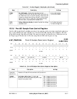
Table 15-7. Control Register Description
Name
Description
Settings
Reserved
Bits 31–28
Reserved—These bits are reserved and should read 0.
ASWB
Bit 27
Auto Mode Switch Bypass
—Controls the switch settings
in Auto XY mode with AZ off. When enabled, switch settings
take the value of SW[7...0], otherwise is determined by
internal logic. This is only for ATE test (debug) purpose.
1 = Bypass enable. Switches are
set by SW[7:0]
0 = Bypass disable. Switches are
set by internal logic
ACAL
Bit 26
Auto Mode Calibration
—Enables/Disables switch settings
for auto-calibration in auto-ZXY mode. Switch settings for X
/ Y are changed from C6 / 39, to CC / 33 respectively.
1 = Enable
0 = Disable
CLKEN
Bit 25
Clock Enable
—Enables/Disables the clock into the Pen
ADC clock generator. This is used to save power when the
Pen ADC is not in use.
0 = Disable clock into the ADC
clock generator
1 = Enable clock into Pen ADC
clock generator
Reserved
Bit 24
Reserved—This bit is reserved and should read 0.
SWRST
Bit 23
Software Reset
—Resets the entire ASP module. All ASP
registers will be restored to default value upon reset.
0 = No effect
1 = Reset -This automatically
restores to 0
Reserved
Bit 22
Reserved—This bit is reserved and should read 0.
U_SEL
Bit 21
U-Channel Resistor Selection
—Selects which external
resistor to use for U-channel measurement.
0 = Resistor at UIN and UIP pins
1 = Resistor at R1a and R2a pins
Summary of Contents for DragonBall MC9328MX1
Page 68: ...1 12 MC9328MX1 Reference Manual MOTOROLA Introduction ...
Page 86: ...2 18 MC9328MX1 Reference Manual MOTOROLA Signal Descriptions and Pin Assignments ...
Page 116: ...3 30 MC9328MX1 Reference Manual MOTOROLA Memory Map ...
Page 126: ...4 10 MC9328MX1 Reference Manual MOTOROLA ARM920T Processor ...
Page 160: ...8 8 MC9328MX1 Reference Manual MOTOROLA System Control ...
Page 272: ...13 32 MC9328MX1 Reference Manual MOTOROLA DMA Controller ...
Page 281: ...Programming Model MOTOROLA Watchdog Timer Module 14 9 ...
Page 282: ...14 10 MC9328MX1 Reference Manual MOTOROLA Watchdog Timer Module ...
Page 300: ...15 18 MC9328MX1 Reference Manual MOTOROLA Analog Signal Processor ASP ...
Page 438: ...18 16 MC9328MX1 Reference Manual MOTOROLA Serial Peripheral Interface Modules SPI 1 and SPI 2 ...
Page 478: ...19 40 MC9328MX1 Reference Manual MOTOROLA LCD Controller ...
Page 574: ...21 32 MC9328MX1 Reference Manual MOTOROLA Memory Stick Host Controller MSHC Module ...
Page 598: ...23 16 MC9328MX1 Reference Manual MOTOROLA Real Time Clock RTC ...
Page 670: ...24 72 MC9328MX1 Reference Manual MOTOROLA SDRAM Memory Controller ...
Page 726: ...25 56 MC9328MX1 Reference Manual MOTOROLA SmartCard Interface Module SIM ...
Page 736: ...26 10 MC9328MX1 Reference Manual MOTOROLA General Purpose Timers ...
Page 854: ...29 18 MC9328MX1 Reference Manual MOTOROLA I2C Module ...
Page 900: ...30 46 MC9328MX1 Reference Manual MOTOROLA Synchronous Serial Interface SSI ...
Page 942: ...32 26 MC9328MX1 Reference Manual MOTOROLA GPIO Module and I O Multiplexer IOMUX ...


