13-4
MC9328MX1 Reference Manual
MOTOROLA
DMA Controller
13.3.1 Big Endian and Little Endian
The BIG_ENDIAN signal determines the MC9328MX1 memory endian configuration. BIG_ENDIAN is a
static pin to the processor and if it is driven logic-high at power on reset the processor's memory system is
configured as big endian. If it is driven logic-low at power on reset the processor's memory system is
configured as little endian. The pin should not be changed after power on reset (POR) deasserts or during
operation.
13.4 Programming Model
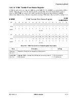
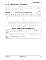
The DMA module includes 107 user-accessible 32-bit registers. These registers are divided into three
groups by function:
•
General registers for all functional blocks (see Section 13.4.1, on page 13-8)
•
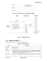
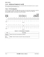
2D memory registers to control the display width and the x and y of the window (see
Section 13.4.2, on page 13-16)
•
Channel registers to control and configure channels 0–10 (see Section 13.4.3, on page 13-18)
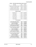
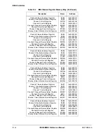
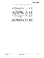
Table 13-2 summarizes these registers and their addresses.
DMA_EOBI
This signal is asserted by the USB device when the last data of the burst is read from the
FIFO.
DMA_EOBI_CNT
This signal is asserted by the USB device when the last data of the burst is read from the
FIFO to indicate the number of valid bytes.
DMA_EOBO
This signal is asserted by the DMA controller when the last data of the burst is written to the
FIFO.
DMA_EOBO_CNT
This signal is asserted by the DMA controller when the last data of the burst is written to the
FIFO to indicate the number of valid bytes.
DMA_ERR
This signal is asserted by DMA controller when any DMA error is detected.
DMA_INT
This signal is asserted by DMA controller when data transfer is complete
—
that is, the data
count reaches the desired level.
Table 13-2. DMA Module Register Memory Map
Description
Name
Address
General Registers
DMA Control Register
DCR
0x00209000
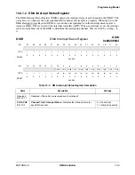
DMA Interrupt Status Register
DISR
0x00209004
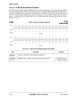
DMA Interrupt Mask Register
DIMR
0x00209008
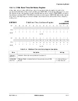
DMA Burst Time-Out Status Register
DBTOSR
0x0020900C
Table 13-1. Signal Description (Continued)
Signal
Description
Summary of Contents for DragonBall MC9328MX1
Page 68: ...1 12 MC9328MX1 Reference Manual MOTOROLA Introduction ...
Page 86: ...2 18 MC9328MX1 Reference Manual MOTOROLA Signal Descriptions and Pin Assignments ...
Page 116: ...3 30 MC9328MX1 Reference Manual MOTOROLA Memory Map ...
Page 126: ...4 10 MC9328MX1 Reference Manual MOTOROLA ARM920T Processor ...
Page 160: ...8 8 MC9328MX1 Reference Manual MOTOROLA System Control ...
Page 272: ...13 32 MC9328MX1 Reference Manual MOTOROLA DMA Controller ...
Page 281: ...Programming Model MOTOROLA Watchdog Timer Module 14 9 ...
Page 282: ...14 10 MC9328MX1 Reference Manual MOTOROLA Watchdog Timer Module ...
Page 300: ...15 18 MC9328MX1 Reference Manual MOTOROLA Analog Signal Processor ASP ...
Page 438: ...18 16 MC9328MX1 Reference Manual MOTOROLA Serial Peripheral Interface Modules SPI 1 and SPI 2 ...
Page 478: ...19 40 MC9328MX1 Reference Manual MOTOROLA LCD Controller ...
Page 574: ...21 32 MC9328MX1 Reference Manual MOTOROLA Memory Stick Host Controller MSHC Module ...
Page 598: ...23 16 MC9328MX1 Reference Manual MOTOROLA Real Time Clock RTC ...
Page 670: ...24 72 MC9328MX1 Reference Manual MOTOROLA SDRAM Memory Controller ...
Page 726: ...25 56 MC9328MX1 Reference Manual MOTOROLA SmartCard Interface Module SIM ...
Page 736: ...26 10 MC9328MX1 Reference Manual MOTOROLA General Purpose Timers ...
Page 854: ...29 18 MC9328MX1 Reference Manual MOTOROLA I2C Module ...
Page 900: ...30 46 MC9328MX1 Reference Manual MOTOROLA Synchronous Serial Interface SSI ...
Page 942: ...32 26 MC9328MX1 Reference Manual MOTOROLA GPIO Module and I O Multiplexer IOMUX ...


