28-34
MC9328MX1 Reference Manual
MOTOROLA
USB Device Port
28.4 Programmer’s Reference
The programmer’s reference guide gives details on how to program the USB module. This section covers
device initialization, processing vendor requests, normal datapath operations, interrupt services, and reset
operation.
28.5 Device Initialization
During device initialization, user software downloads critical configuration information to the UDC
module and prepares the USB module datapath for processing. This process is performed at two different
times: at reset (hard reset or software reset via RST bit in the USB_DDAR register) and when the device is
first connected to the USB.
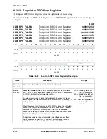
USB_EP0_FWRP
USB_EP1_FWRP
USB_EP2_FWRP
USB_EP3_FWRP
USB_EP4_FWRP
USB_EP5_FWRP
Endpoint 0 FIFO Write Pointer Register
Endpoint 1 FIFO Write Pointer Register
Endpoint 2 FIFO Write Pointer Register
Endpoint 3 FIFO Write Pointer Register
Endpoint 4 FIFO Write Pointer Register
Endpoint 5 FIFO Write Pointer Register
Addr
0x00212058
0x00212088
0x002120B8
0x002120E8
0x00212118
0x00212148
BIT
31
30
29
28
27
26
25
24
23
22
21
20
19
18
17
16
TYPE
r
r
r
r
r
r
r
r
r
r
r
r
r
r
r
r
RESET
0
0
0
0
0
0
0
0
0
0
0
0
0
0
0
0
0x0000
BIT
15
14
13
12
11
10
9
8
7
6
5
4
3
2
1
0
WP
TYPE
r
r
r
r
r
r
r
r
r
r
rw
rw
rw
rw
rw
rw
RESET
0
0
0
0
0
0
0
0
0
0
0
0
0
0
0
0
0x0000
Table 28-24. Endpoint n FIFO Write Pointer Registers Description
Name
Description
Reserved
Bits 31–6
Reserved—These bits are reserved and should read 0.
WP
Bits 5
–
0
Write Pointer
—Points to the next FIFO location to write. The physical address of this FIFO location is
actually the sum of the read pointer and the FIFO base, provided through a port to the FIFO controller.
This base address can vary, however if chosen properly, the FIFO RAM address can be concatenated
with the read pointer instead of requiring hardware for addition. The read pointer can be both read and
written. This ability facilitates the debugging of the FIFO controller and peripheral drivers.
Summary of Contents for DragonBall MC9328MX1
Page 68: ...1 12 MC9328MX1 Reference Manual MOTOROLA Introduction ...
Page 86: ...2 18 MC9328MX1 Reference Manual MOTOROLA Signal Descriptions and Pin Assignments ...
Page 116: ...3 30 MC9328MX1 Reference Manual MOTOROLA Memory Map ...
Page 126: ...4 10 MC9328MX1 Reference Manual MOTOROLA ARM920T Processor ...
Page 160: ...8 8 MC9328MX1 Reference Manual MOTOROLA System Control ...
Page 272: ...13 32 MC9328MX1 Reference Manual MOTOROLA DMA Controller ...
Page 281: ...Programming Model MOTOROLA Watchdog Timer Module 14 9 ...
Page 282: ...14 10 MC9328MX1 Reference Manual MOTOROLA Watchdog Timer Module ...
Page 300: ...15 18 MC9328MX1 Reference Manual MOTOROLA Analog Signal Processor ASP ...
Page 438: ...18 16 MC9328MX1 Reference Manual MOTOROLA Serial Peripheral Interface Modules SPI 1 and SPI 2 ...
Page 478: ...19 40 MC9328MX1 Reference Manual MOTOROLA LCD Controller ...
Page 574: ...21 32 MC9328MX1 Reference Manual MOTOROLA Memory Stick Host Controller MSHC Module ...
Page 598: ...23 16 MC9328MX1 Reference Manual MOTOROLA Real Time Clock RTC ...
Page 670: ...24 72 MC9328MX1 Reference Manual MOTOROLA SDRAM Memory Controller ...
Page 726: ...25 56 MC9328MX1 Reference Manual MOTOROLA SmartCard Interface Module SIM ...
Page 736: ...26 10 MC9328MX1 Reference Manual MOTOROLA General Purpose Timers ...
Page 854: ...29 18 MC9328MX1 Reference Manual MOTOROLA I2C Module ...
Page 900: ...30 46 MC9328MX1 Reference Manual MOTOROLA Synchronous Serial Interface SSI ...
Page 942: ...32 26 MC9328MX1 Reference Manual MOTOROLA GPIO Module and I O Multiplexer IOMUX ...


