Programming Model
MOTOROLA
Synchronous Serial Interface (SSI)
30-13
30.3.6 SSI Receive Shift Register
The SSI Receive Shift Register (RXSR) is a 16-bit shift register that contains the data being received from
the SSI_RXDAT pin. When the register is full, received data fills the receive FIFO.
When a continuous clock is used, data is shifted in by the selected (internal/external) bit clock when the
associated (internal/external) frame sync is asserted. When a gated clock is used, data is shifted in from the
SSI_TXDAT pin by the selected (internal/external) gated clock.
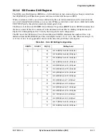
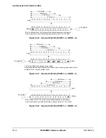
The Receive shift direction (RSHFD) bit and Receive bit position(RXBIT0) in the SRCR determines how
the data is stored. Table 30-6 contains all of the information about data bit shifting configurations and
Figure 30-10 through Figure 30-13 visually the data path for each configuration.
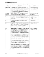
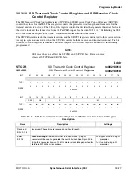
The WL bits in the SSI Receive Clock Control Register (SRCCR) determine the number of bits to be
shifted in from the SSI_RXDAT pin. This word length can be 8, 10, 12, or 16 bits. When receiving 8, 10,
or 12 bits of data, 0s are appended to the end of the data string to fill the 16-bit register.
Table 30-6. Data Bit Shifting Configuration
RXBIT0
RSHFD
WL[1:0]
Shifting to bit
0
0
00
Bit 15 (MSB) first, bit 8 (LSB) last
01
Bit 15 (MSB) first, bit 6 (LSB) last
10
Bit 15 (MSB) first, bit 4 (LSB) last
11
Bit 15 (MSB) first, bit 0 (LSB) last
0
1
00
Bit 8 (MSB) first, bit 15 (LSB) last
01
Bit 6 (MSB) first, bit 15 (LSB) last
10
Bit 4 (MSB) first, bit 15 (LSB) last
11
Bit 0 (MSB) first, bit 15 (LSB) last
1
0
00
Bit 0 (MSB) first, bit 7 (LSB) last
01
Bit 0 (MSB) first, bit 9 (LSB) last
10
Bit 0 (MSB) first, bit 11 (LSB) last
11
Bit 0 (MSB) first, bit 15 (LSB) last
1
1
00
Bit 7 (MSB) first, bit 0 (LSB) last
01
Bit 9 (MSB) first, bit 0 (LSB) last
10
Bit 11 (MSB) first, bit 0 (LSB) last
11
Bit 15 (MSB) first, bit 0 (LSB) last
Summary of Contents for DragonBall MC9328MX1
Page 68: ...1 12 MC9328MX1 Reference Manual MOTOROLA Introduction ...
Page 86: ...2 18 MC9328MX1 Reference Manual MOTOROLA Signal Descriptions and Pin Assignments ...
Page 116: ...3 30 MC9328MX1 Reference Manual MOTOROLA Memory Map ...
Page 126: ...4 10 MC9328MX1 Reference Manual MOTOROLA ARM920T Processor ...
Page 160: ...8 8 MC9328MX1 Reference Manual MOTOROLA System Control ...
Page 272: ...13 32 MC9328MX1 Reference Manual MOTOROLA DMA Controller ...
Page 281: ...Programming Model MOTOROLA Watchdog Timer Module 14 9 ...
Page 282: ...14 10 MC9328MX1 Reference Manual MOTOROLA Watchdog Timer Module ...
Page 300: ...15 18 MC9328MX1 Reference Manual MOTOROLA Analog Signal Processor ASP ...
Page 438: ...18 16 MC9328MX1 Reference Manual MOTOROLA Serial Peripheral Interface Modules SPI 1 and SPI 2 ...
Page 478: ...19 40 MC9328MX1 Reference Manual MOTOROLA LCD Controller ...
Page 574: ...21 32 MC9328MX1 Reference Manual MOTOROLA Memory Stick Host Controller MSHC Module ...
Page 598: ...23 16 MC9328MX1 Reference Manual MOTOROLA Real Time Clock RTC ...
Page 670: ...24 72 MC9328MX1 Reference Manual MOTOROLA SDRAM Memory Controller ...
Page 726: ...25 56 MC9328MX1 Reference Manual MOTOROLA SmartCard Interface Module SIM ...
Page 736: ...26 10 MC9328MX1 Reference Manual MOTOROLA General Purpose Timers ...
Page 854: ...29 18 MC9328MX1 Reference Manual MOTOROLA I2C Module ...
Page 900: ...30 46 MC9328MX1 Reference Manual MOTOROLA Synchronous Serial Interface SSI ...
Page 942: ...32 26 MC9328MX1 Reference Manual MOTOROLA GPIO Module and I O Multiplexer IOMUX ...


