Pin Configuration for GPIO
MOTOROLA
GPIO Module and I/O Multiplexer (IOMUX)
32-5
set of these signals available for each GPIO Port (Port A, Port B, Port C, and Port D). The “IN” signals
denote inputs to the GPIO module whereas the “OUT” signals are outputs from the GPIO module, as can
be seen in Figure 32-2 on page 32-4. In the case of the “IN” signals, these signals are passed through the
GPIO module from the selected peripheral and are output to the MC9328MX1 pins. Therefore, the Data
Direction Register for the desired “IN” signal must be set as an output. On the other hand, in the case of the
“OUT” signals, these signals are also passed through the GPIO module, however their inputs come from
the MC9328MX1 pins and are output to the selected peripheral. Therefore, the Data Direction register for
the desired “OUT” signal must be set as an input. For example, if the user wishes to route the SPI2_RXD
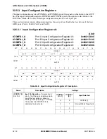
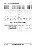
input via the PA17 pin, they would need to set GIUS_A bit 1 for GPIO function (set bit 1). The next step
would then be to set the ICONFA1_A bits 2 and 3 (to 11) to select the GPIO-IN to allow PA1 to drive
AOUT[1]. Finally, the DDIR bit 1 must be set as an input (clear bit 1). Should the user wish to route the
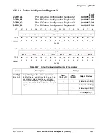
SPI2_CLK output via pin PD7, they should first set bit 7 of GIUS_D. The next step would be to clear bits
15 and 14 of OCR1_D to select AIN[7] as an input to the GPIO module. Finally, bit 7 of DDIR must be set
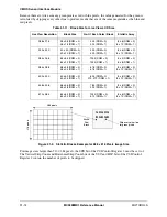
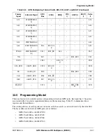
to select this signal as an output from the GPIO module to the external pin. Table 32-3 shows the signals
that use this expanded functionality.
Table 32-2. Pin Configuration
Pin
Configuration Procedure
Port A
Pins 31–0
1.
For each pin [i] that is used as a GPIO, set bit [i] in the Port A GPIO In Use Register (GIUS_A).
2.
When pin [i] is used as an input:
•
Clear bit [i] in the Port A Data Direction Register (DDIR_A)
•
Read the Port A Sample Status Register (SSR_A) as needed
3.
When pin [i] is used as an output:
•
Set bits [2i + 1] and [2i] in the Port A Output Configuration Register 1 (OCR1_A)
or
Set bits [2i – 32 + 1] and [2i – 32] in the Port A Output Configuration Register 2 (OCR2_A)
•
Write desired output value to bit [i] of the Port A Data Register (DR_A)
•
Set bit [i] in the Port A Data Direction Register (DDIR_A)
Port B
Pins 31–0
1.
For each pin [i] that is used as a GPIO, set bit [i] in thePort B GPIO In Use Register (GIUS_B).
2.
When pin [i] is used as an input:
•
Clear bit [i] in the Port B Data Direction Register (DDIR_B)
•
Read the Port B Sample Status Register (SSR_B) as needed
3.
When pin [i] is used as an output:
•
Set bits [2i + 1] and [2i] in the Port B Output Configuration Register 1 (OCR1_B)
or
Set bits [2i – 32 + 1] and [2i – 32] in the Port B Output Configuration Register 2 (OCR2_B)
•
Write desired output value to bit [i] of the Port B Data Register (DR_B)
•
Set bit [i] in the Port B Data Direction Register (DDIR_B)
Port C
Pins 31–0
1.
For each pin [i] that is used as a GPIO, set bit [i] in the Port C GPIO In Use Register (GIUS_C).
2.
When pin [i] is used as an input:
•
Clear bit [i] in the Port C Data Direction Register (DDIR_C)
•
Read the Port C Sample Status Register (SSR_C) as needed
3.
When pin [i] is used as an output:
•
Set bits [2i + 1] and [2i] in the Port C Output Configuration Register 1 (OCR1_C)
or
Set bits [2i – 32 + 1] and [2i – 32] in the Port C Output Configuration Register 2 (OCR2_C)
•
Write desired output value to bit [i] of the Port C Data Register (DR_C)
•
Set bit [i] in the Port C Data Direction Register (DDIR_C)
Summary of Contents for DragonBall MC9328MX1
Page 68: ...1 12 MC9328MX1 Reference Manual MOTOROLA Introduction ...
Page 86: ...2 18 MC9328MX1 Reference Manual MOTOROLA Signal Descriptions and Pin Assignments ...
Page 116: ...3 30 MC9328MX1 Reference Manual MOTOROLA Memory Map ...
Page 126: ...4 10 MC9328MX1 Reference Manual MOTOROLA ARM920T Processor ...
Page 160: ...8 8 MC9328MX1 Reference Manual MOTOROLA System Control ...
Page 272: ...13 32 MC9328MX1 Reference Manual MOTOROLA DMA Controller ...
Page 281: ...Programming Model MOTOROLA Watchdog Timer Module 14 9 ...
Page 282: ...14 10 MC9328MX1 Reference Manual MOTOROLA Watchdog Timer Module ...
Page 300: ...15 18 MC9328MX1 Reference Manual MOTOROLA Analog Signal Processor ASP ...
Page 438: ...18 16 MC9328MX1 Reference Manual MOTOROLA Serial Peripheral Interface Modules SPI 1 and SPI 2 ...
Page 478: ...19 40 MC9328MX1 Reference Manual MOTOROLA LCD Controller ...
Page 574: ...21 32 MC9328MX1 Reference Manual MOTOROLA Memory Stick Host Controller MSHC Module ...
Page 598: ...23 16 MC9328MX1 Reference Manual MOTOROLA Real Time Clock RTC ...
Page 670: ...24 72 MC9328MX1 Reference Manual MOTOROLA SDRAM Memory Controller ...
Page 726: ...25 56 MC9328MX1 Reference Manual MOTOROLA SmartCard Interface Module SIM ...
Page 736: ...26 10 MC9328MX1 Reference Manual MOTOROLA General Purpose Timers ...
Page 854: ...29 18 MC9328MX1 Reference Manual MOTOROLA I2C Module ...
Page 900: ...30 46 MC9328MX1 Reference Manual MOTOROLA Synchronous Serial Interface SSI ...
Page 942: ...32 26 MC9328MX1 Reference Manual MOTOROLA GPIO Module and I O Multiplexer IOMUX ...


