Appendix D – GTXI Buffer Board
155
IA Name Description
Default
Value
2
MSA
Memory Start Address for
MEMS0
xx00
3
MEA
Memory End Address for
MEMS0
xx00
4
MMR
Memory Mask Register and
enable mode
xx00
5
DMR
DMA Mask Register
xx00
6
IMR
IRQ Mask Register
xx00
Table D-2: Internal Address Register Descriptions
I/O Space
The basic PC I/O space is 1kbyte - 000h-3FFh. The GTXI buffer
divides this space into blocks. Some of these blocks can be assigned
to the GTXI by writing to the IOM0 and IOM1 registers. The power
up default I/O space is addresses 200-23Fh and 300-33Fh.
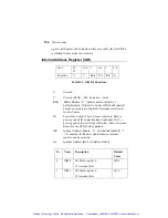
I/O Mask Register 0 (IOM0)
Internal address (IA) is 0.
Bit #
15-12
11-0
Function U
IOE11-IOE0
Table D-3: I/O Mask Register 0 Bit Functions
U
Unused
IOE
I/O block enable. ‘0’ - block disabled. ‘1’ - block enabled.
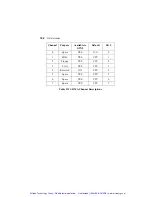
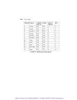
See the table on the next page for bit assignments.
The default value for bits 11-0 is 000h (all disabled).
Artisan Technology Group - Quality Instrumentation ... Guaranteed | (888) 88-SOURCE | www.artisantg.com


