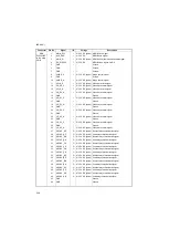

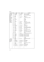
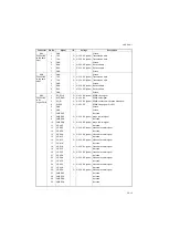

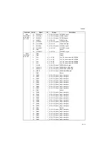

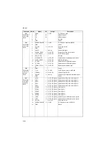


2KR/2KS
2-3-19
YC9
21
EXTBOEN
O
0/3.3 V DC (pulse) EXTBOEN signal
Connected
to the inter-
face PWB
22
CFWEN0
O
0/3.3 V DC (pulse) CFWEN0 signal
23
EXTBDIR
O
0/3.3 V DC (pulse) EXTBDIR signal
24
CFRST0
O
0/3.3 V DC
CFRST0 signal
25
CF0CSN0
O
0/3.3 V DC (pulse) CF0CSN0 signal
26
CFWAITN0
I
0/3.3 V DC
CFWAITN0 signal
27
CF0CSN1
O
0/3.3 V DC (pulse) CF0CSN1 signal
28
CF0CDET1
I
0/3.3 V DC
CF0CDET1 signal
29
GND
-
-
Ground
30
CF0CDET2
I
0/3.3 V DC
CF0CDET2 signal
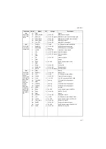
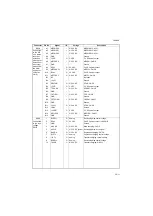
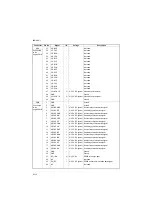
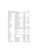
YC10
1
GND
-
-
Ground
Connected
to the DP
2
GND
-
-
Ground
3
3.3V
O
3.3 V DC
3.3 V DC power output to DPRPWB
4
3.3V
O
3.3 V DC
3.3 V DC power output to DPRPWB
5
3.3V
O
3.3 V DC
3.3 V DC power output to DPRPWB
6
3.3V
O
3.3 V DC
3.3 V DC power output to DPRPWB
7
VCLKB
I
0/3.3 V DC (pulse) DPRPWB clock signal
8
VSYNCB
I
0/3.3 V DC (pulse) DPRPWB VSYNCB signal
9
HSYNCB
I
0/3.3 V DC (pulse) DPRPWB HSYNCB signal
10
MREB
I
0/3.3 V DC (pulse) DPRPWB MREB signal
11
GND
-
-
Ground
12
DRB0
I
0/3.3 V DC (pulse) Image data signal
13
DRB1
I
0/3.3 V DC (pulse) Image data signal
14
DRB2
I
0/3.3 V DC (pulse) Image data signal
15
DRB3
I
0/3.3 V DC (pulse) Image data signal
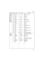
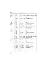
16
DRB4
I
0/3.3 V DC (pulse) Image data signal
17
DRB5
I
0/3.3 V DC (pulse) Image data signal
18
DRB6
I
0/3.3 V DC (pulse) Image data signal
19
DRB7
I
0/3.3 V DC (pulse) Image data signal
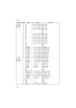
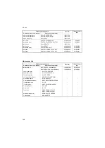
20
GND
-
-
Ground
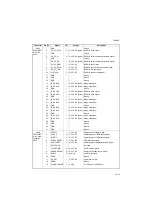
21
DGB0
I
0/3.3 V DC (pulse) Image data signal
22
DGB1
I
0/3.3 V DC (pulse) Image data signal
23
DGB2
I
0/3.3 V DC (pulse) Image data signal
24
DGB3
I
0/3.3 V DC (pulse) Image data signal
25
DGB4
I
0/3.3 V DC (pulse) Image data signal
26
DGB5
I
0/3.3 V DC (pulse) Image data signal
27
DGB6
I
0/3.3 V DC (pulse) Image data signal
28
DGB7
I
0/3.3 V DC (pulse) Image data signal
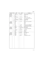
29
GND
-
-
Ground
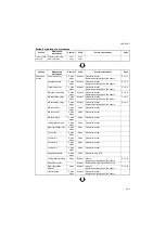
30
DBB0
I
0/3.3 V DC (pulse) Image data signal
31
DBB1
I
0/3.3 V DC (pulse) Image data signal
32
DBB2
I
0/3.3 V DC (pulse) Image data signal
33
DBB3
I
0/3.3 V DC (pulse) Image data signal
34
DBB4
I
0/3.3 V DC (pulse) Image data signal
35
DBB5
I
0/3.3 V DC (pulse) Image data signal
Connector
Pin No.
Signal
I/O
Voltage
Description
Содержание TASKalfa 420i
Страница 1: ...SERVICE MANUAL Published in May 2010 842KS113 2KSSM063 Rev 3 TASKalfa 420i TASKalfa 520i ...
Страница 4: ...This page is intentionally left blank ...
Страница 10: ...This page is intentionally left blank ...
Страница 14: ...2KR 2KS This page is intentionally left blank ...
Страница 224: ...2KR 2KS 1 4 66 This page is intentionally left blank ...
Страница 328: ...2KR 2KS 2 3 30 This page is intentionally left blank ...
Страница 371: ...INSTALLATION GUIDE FOR PAPER FEEDER ...
Страница 381: ...INSTALLATION GUIDE FOR 3000 SHEETS PAPER FEEDER ...
Страница 436: ...INSTALLATION GUIDE FOR CENTER FOLDING UNIT ...
Страница 450: ...INSTALLATION GUIDE FOR MAILBOX ...
Страница 458: ...INSTALLATION GUIDE FOR HOLE PUNCH UNIT ...
Страница 470: ...INSTALLATION GUIDE FOR BUILT IN FINISHER ...
Страница 483: ...INSTALLATION GUIDE FOR JOB SEPARATOR ...
Страница 491: ...INSTALLATION GUIDE FOR FAX System ...
Страница 507: ......
Страница 508: ......


