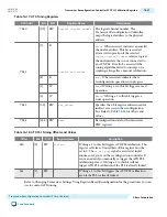
Reconfig Addr
Bits
R/W
Register Name
Description
7’h44
[15:0] RW
data
Specifies the read or write data.
Note: All undefined register bits are reserved.
Table 16-20: PLL Reconfiguration Offsets and Values
Offset
Bits
R/W
Name
Description
0x0
[2:0]
RW
logical refclk selection
When written initiates reference clock
change to the logical reference clock
indexed by bits [2:0].
This index refers to the Number of
input clocks on the Reconfiguration
tab. You can specify up to 5 input
clocks. When performing a reference
clock switch for an ATX PLL you
must stream in an ATX MIF.
This offset is used to switch the
reference clock for CMU PLLs. To
perform a reference clock switch for
ATX PLLs use MIF mode 0 and
stream the ATX PLL MIF.
0x1
[2:0]
RW
logical PLL selection
When written initiates a clock
generation block (CGB) switch to
logical PLL indexed by bits [2:0].
This index refers to the Number of
TX PLLs selected on the Reconfigu‐
ration tab. You can specify up to 4
input clocks. If you set the Main TX
PLL logical index to 0, the Quartus II
software initializes your design using
the first PLL defined.
0x2
[24:0] RO
refclk physical mapping
Specifies the logical to physical refclk
for current logical channel.
0x3
[14:0] RO
PLL physical mapping
Specifies the logical to physical clock
generation block word for current
logical channel.
Transceiver Reconfiguration Controller DCD Calibration Registers
UG-01080
2015.01.19
Transceiver Reconfiguration Controller DCD Calibration Registers
16-31
Transceiver Reconfiguration Controller IP Core Overview
Altera Corporation
Send Feedback


