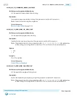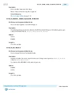
Options
• AC_COUPLING
• DC_COUPLING_INTERNAL_100_OHMS
• DC_COUPLING_EXTERNAL_RESISTOR
Assign To
Pin - PLL refclk pin
XCVR_RX_BYPASS_EQ_STAGES_234
Pin Planner and Assignment Editor Name
Receiver Equalizer Stage 2, 3, 4 Bypass
Description
Bypass continuous time equalizer stages 2, 3, and 4 to save power. This setting eliminates significant AC
gain on the equalizer and is appropriate for chip-to-chip short range communication on a PCB. Assigning
a value to this setting and
XCVR_ANALOG_SETTINGS_PROTOCOL
results in a Quartus II Fitter error as shown
in the following example:
Error (21215)
Error resolving parameter "pm_rx_sd_bypass_eqz_stages_234" value
on instance "pci_interface_ddf2:u_pci_interface_2|
PCIE_8x8Gb_HARDIP_2:PCIe2_Interface.U_PCIE_CORE|
altpcie_sv_hip_ast_hwtcl:pcie_8x8gb_hardip_2_inst|
altpcie_hip_256_pipen1b:altpcie_hip_256_pipen1b
|sv_xcvr_pipe_native:g_xcvr.sv_xcvr_pipe_native|sv_xcvr_native:
inst_sv_xcvr_native|sv_pma:inst_sv_pma|sv_rx_pma:rx_pma.
sv_rx_pma_inst|rx_pmas[8].rx_pma.rx_pma_buf": Only one QSF
setting for the parameter is allowed.
Options
• All_Stages_Enabled
• Bypass_Stages
Assign To
Pin - RX serial data
Note: This setting can be used for data rates upto 5 Gbps for backplane applications, and 8 Gbps for chip-
to-chip applications.
XCVR_TX_SLEW_RATE_CTRL
Pin Planner and Assignment Editor Name
Transmitter Slew Rate Control
19-36
XCVR_RX_BYPASS_EQ_STAGES_234
UG-01080
2015.01.19
Altera Corporation
Analog Parameters Set Using QSF Assignments
Send Feedback


