Parameter
Range
Description
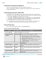
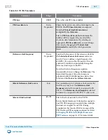
Enable rx_std_rmfifo_
full port
On/Off
When you turn this option On, the rate match FIFO
outputs a FIFO full status flag.
Related Information
Transceiver Architecture in Arria V Devices
Byte Ordering Block Parameters
This section describes the byte ordering block parameters.
The RX byte ordering block realigns the data coming from the byte deserializer. This block is necessary
when the PCS to FPGA fabric interface width is greater than the PCS datapath. Because the timing of the
RX PCS reset logic is indeterminate, the byte ordering at the output of the byte deserializer may or may
not match the original byte ordering of the transmitted data.
Note: For more information refer to the Byte Ordering section in the
Transceiver Architecture in Arria V
Devices
.
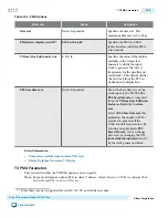
Table 13-12: Byte Ordering Block Parameters
Parameter
Range
Description
Enable RX byte
ordering
On/Off
When you turn this option On, the PCS includes the byte
ordering block.
Byte ordering
control mode
manual
auto
Specifies the control mode for the byte ordering block. The
following modes are available:
• Manual: Allows you to control the byte ordering block
• Auto: The word aligner automatically controls the byte
ordering block once word alignment is achieved.
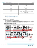
Byte ordering
pattern width
8–10
Shows width of the pattern that you must specify. This width
depends upon the PCS width and whether or not 8B/10B
encoding is used as follows:
Width
8, 16,32
10,20,40
8,16,32
8B/10B
No
No
Yes
Pad Pattern
8 bits
10 bits
9 bits
Byte ordering
symbol count
1–2
Specifies the number of symbols the word aligner should search
for. When the PMA is 16 or 20 bits wide, the byte ordering block
can optionally search for 1 or 2 symbols.
UG-01080
2015.01.19
Byte Ordering Block Parameters
13-13
Arria V Transceiver Native PHY IP Core
Altera Corporation
Send Feedback


