Name
Value
Description
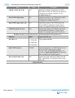
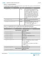
Data rate
Device Dependent If you select a data rate that is not supported by the
configuration you have specified, the MegaWizard
displays a error message in the message pane.
Table 11-7
for sample the channel widths that support these data
rates.
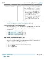
Base data rate
1 × Data rate
2 × Data rate
4 × Data rate
8 × Data rate
For systems that transmit and receive data at more than
one data rate, select a base data rate that minimizes the
number of PLLs required to generate the clocks for data
transmission. The Recommended Base Data Rate and
Clock Divisors for CPRI table lists the recommended
Base data rates for various Data rates.
The available options are dynamically computed based
on the Data rate you specified as long as those Base data
rates are within the frequency range of the PLL.
Input clock frequency
Data rate/20
Data rate/10
Data rate/8
Data rate/5
Data rate/4
Data rate/2.5
Data rate/2
Data rate/1.25
Data rate/1
This is the reference clock for the PHY PLL. The
available options are based on the Base data rate
specified.
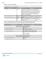
Enable tx_clkout
feedback path for TX
PLL
On/ Off
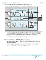
When On, the core uses TX PLL feedback to align the
TX core clock with the source to the TX PLL which is the
RX recovered clock. This configuration is shown in
Using TX PLL Feedback to Align the TX Core Clock
with the RX Core Clock.
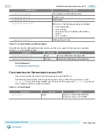
The following table lists the available channel widths available at selected frequencies. The channel width
options are restricted by the following maximum FPGA-PCS fabric interface frequencies:
• Arria V devices—153.6 MHz
• Cyclone V devices—153.6 MHz
• Stratix V devices—221 MHz
Table 11-7: Sample Channel Width Options for Supported Serial Data Rates
Serial Data Rate (Mbps)
Channel Width (FPGA-PCS Fabric)
Single-Width
Double-Width
8-Bit
16-Bit
16-Bit
32-Bit
614.4
Yes
Yes
No
No
UG-01080
2015.01.19
General Options Parameters for Deterministic Latency PHY
11-9
Deterministic Latency PHY IP Core
Altera Corporation
Send Feedback


