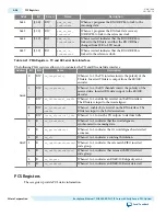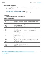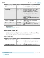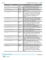
Table 5-6: Clock and Reset Signals
Signal Name
Direction
Description
rx_recovered_clk
Output
The RX clock which is recovered from the received
data. You can use this clock as a reference to lock an
external clock source. Its frequency is 125 or 156.25
MHz. For 10G PCS, its frequency is 257.8125 MHz.
tx_clkout_1g
Output
GMII TX clock for the 1G TX and RX parallel data
source interface. The frequency is 125 MHz.
rx_clkout_1g
Output
GMII RX clock for the 1G RX parallel data source
interface. The frequency is 125 MHz.
rx_coreclkin_1g
Input
Clock to drive the read side of the RX phase
compensation FIFO in the Standard PCS. The
frequency is 125 MHz.
tx_coreclkin_1g
Input
Clock to drive the write side of the TX phase
compensation FIFO in the Standard PCS. The
frequency is 125 MHz.
pll_ref_clk_1g
Input
Reference clock for the PMA block for the 1G
mode. Its frequency is 125 or 62.5 MHz.
pll_ref_clk_10g
Input
Reference clock for the PMA block in 10G mode. Its
frequency is 644.53125 or 322.265625 MHz.
pll_powerdown_1g
Input
Resets the 1Gb TX PLLs.
pll_powerdown_10g
Input
Resets the 10Gb TX PLLs.
tx_analogreset
Input
Resets the analog TX portion of the transceiver
PHY.
tx_digitalreset
Input
Resets the digital TX portion of the transceiver
PHY.
rx_analogreset
Input
Resets the analog RX portion of the transceiver
PHY.
rx_digitalreset
Input
Resets the digital RX portion of the transceiver
PHY.
usr_seq_rest
Input
Resets the sequencer.
1G/10GbE PHY Data Interfaces
The following table describes the signals in the XGMII and GMII interfaces. The MAC drives the TX
XGMII and GMII signals to the 1G/10GbE PHY. The 1G/10GbE PHY drives the RX XGMII or GMII
signals to the MAC.
Table 5-7: SGMII and GMII Signals
Signal Name
Direction
Description
1G/10GbE XGMII Data Interface
UG-01080
2015.01.19
1G/10GbE PHY Data Interfaces
5-9
1G/10 Gbps Ethernet PHY IP Core
Altera Corporation
Send Feedback


