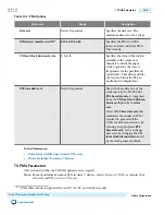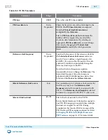
Table 13-5: TX PLL Parameters
Parameter
Range
Description
PLL type
CMU
This is the only PLL type available.
PLL base data rate
Device
Dependent
Shows the base data rate of the clock input to the
TX PLL.The PLL base data rate is computed
from the TX local clock division factor
multiplied by the Data rate.
Select a PLL base data rate that minimizes the
number of PLLs required to generate all the
clocks for data transmission. By selecting an
appropriate PLL base data rate, you can change
data rates by changing the TX local clock
division factor used by the clock generation
block.
Reference clock frequency
Device
Dependent
Specifies the frequency of the reference clock for
the Selected reference clock source index you
specify. You can define a single frequency for
each PLL. You can use the Transceiver Reconfi‐
guration Controller to dynamically change the
reference clock input to the PLL.
Note that the list of frequencies updates
dynamically when you change the Data rate. The
Input clock frequency drop down menu is
populated with all valid frequencies derived as a
function of the Data rate and Base data rate.
Selected reference clock source
0–4
You can define up to 5 reference clock sources for
the PLLs in your core. The Reference clock
frequency selected for index 0, is assigned to TX
PLL<0>. The Reference clock frequency selected
for index 1, is assigned to TX PLL<1>, and so on.
Selected clock network
x1 ×N
Selects the clock network for the TX PLL.
In non-bonded mode, each channel is assigned to
one PLL. PLL merging is required when multiple
channels are assigned to one PLL. During
compilation, the Quartus II Fitter, merges all the
PLLs that meet PLL merging requirements. Refer
to
Merging TX PLLs In Multiple Transceiver
PHY Instances
on page 16-57 for more details.
UG-01080
2015.01.19
TX PLL Parameters
13-7
Arria V Transceiver Native PHY IP Core
Altera Corporation
Send Feedback


