660
Chapter 16
Clocked Serial Interface B (CSIB)
User’s Manual U16580EE3V1UD00
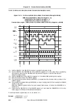
16.4.6 Continuous mode (master mode, reception mode)
Figure 16-14:
Continuous Mode (Master Mode, Reception Mode)
MSB First (CBnDIR Bit of CBnCTL0 Register = 0),
CBnCKP Bit of the CBnCTL1 Register = 0,
CBnDAP Bit of the CBnCTL1 Register = 1,
Transfer Data Length = 8 Bits (CSnCL3 to CBnCL0 Bits of CBnCTL2 Register = 0000B)
<1> Set the CBnCTL1 and CBnCTL2 registers to specify the transfer mode.
<2> Set the CBnRXE bit of the CBnCTL0 register to 1 at the same time as specifying the transfer
mode using the CBnDIR bit of the CBnCTL0 register, to set the reception enabled status.
<3> Set the CBnPWR bit of the CBnCTL0 register is 1 to enable CSIB operating clock supply.
<4> Perform a dummy read of the CBnRX register (reception start trigger).
<5> The reception complete interrupt (INTCBnR) is output, notifying the CPU that reading the CBnRX
(CBnRXL) register is possible. Read the CBnRX register before the next receive data arrives or
before the CBnPWR bit is cleared to 0.
<6> Clear the CBnSCE bit of the CBnCTL0 register is 0 to set the reception end data status.
<7> Check that the CBnTSF bit of the CBnSTR register is 0 and clear the CBnPWR bit to 0 to stop
clock supply to CSIB (end of reception).
To continue transfer, repeat steps <4> and <5> before <6>.
Remark:
μ
PD70F3187: n = 0, 1
μ
PD70F3447: n = 0
<1>
<2>
<3>
<7>
<5>
<5>
<6>
<4>
1
0
0
0
0
0
0
0
1
1
1
1
1
55H
SCKBn pin
CBnSCE bit
SIBn pin
INTCnR
signal
Shift
register n
CBnRX
register
1
1
0
55H
AAH
AAH
00H
00H
Summary of Contents for V850E/PH2
Page 6: ...6 Preface User s Manual U16580EE3V1UD00...
Page 16: ...16 User s Manual U16580EE3V1UD00...
Page 28: ...28 User s Manual U16580EE3V1UD00...
Page 32: ...32 User s Manual U16580EE3V1UD00...
Page 84: ...84 Chapter 2 Pin Functions User s Manual U16580EE3V1UD00 MEMO...
Page 144: ...144 Chapter 3 CPU Functions User s Manual U16580EE3V1UD00 MEMO...
Page 192: ...192 Chapter 5 Memory Access Control Function PD70F3187 only User s Manual U16580EE3V1UD00 MEMO...
Page 312: ...312 Chapter 9 16 Bit Timer Event Counter P User s Manual U16580EE3V1UD00 MEMO...
Page 534: ...534 Chapter 11 16 bit Timer Event Counter T User s Manual U16580EE3V1UD00...
Page 969: ...969 Chapter 20 Port Functions User s Manual U16580EE3V1UD00 MEMO...
Page 970: ...970 Chapter 20 Port Functions User s Manual U16580EE3V1UD00...
Page 976: ...976 Chapter 22 Internal RAM Parity Check Function User s Manual U16580EE3V1UD00 MEMO...
Page 984: ...984 Chapter 23 On Chip Debug Function OCD User s Manual U16580EE3V1UD00 MEMO...
Page 1006: ...1006 Chapter 24 Flash Memory User s Manual U16580EE3V1UD00 MEMO...
Page 1036: ...1036 Chapter 27 Recommended Soldering Conditions User s Manual U16580EE3V1UD00 MEMO...
Page 1046: ...1046 Appendix A Index User s Manual U16580EE3V1UD00 MEMO...
Page 1052: ...1052 User s Manual U16580EE3V1UD00...
Page 1053: ......


