background image

208

Chapter 6

DMA Functions (DMA Controller)

User’s Manual U16580EE3V1UD00

6.4.3  DMA transfer of serial interfaces

(1)

Serial data reception with DMA transfer

The DMAC has two dedicated channels (4 and 5) to support the serial data reception. Each of

both channels can be assigned to a serial interface (CSI30, CSI31

Note

, CSIB0, CSIB1

Note

,

UARTC0, UARTC1). As DMA trigger factor, which requests and starts the DMA transfer, the corre-
sponding interrupt signal at the end of reception is pre-defined (ref. to Table 6-2).

For each DMA trigger the data will be transferred from the corresponding serial reception register
to internal RAM. Depending on the serial interface the transfer data size can be set to 8 or 16 bits
(refer to Table 6-2)

In case of 8 bits transfer data size, the destination address is incremented by 1 for each 
occurrence of DMA trigger. When selecting 16 bits transfer data size the destination address must
be even, and is incremented by 2 for each DMA trigger.

When the DMA transfer count of a DMA channel terminates, the DMA transfer is stopped and a
DMA completion interrupt is generated. The maximum DMA transfer count is 256.

Note:

Not available on 

μ

PD70F3447.

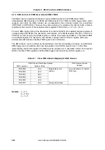
Table 6-2:

DMA Configuration of Serial Data Reception

Serial Interface

DMA Trigger 

Factor

Transfer Data 

Size

Source

Destination

CSI30

INTC30

8 bits

SIRB0L

Any iRAM address

16 bits

SIRB0

Any even iRAM address

CSI31

Note

INTC31

8 bits

SIRB1L

Any iRAM address

16 bits

SIRB1

Any even iRAM address

CSIB0

INTCB0T

8 bits

CB0RXL

Any iRAM address

16 bits

CB0RX

Any even iRAM address

CSIB1

Note

INTCB1T

8 bits

CB1RXL

Any iRAM address

16 bits

CB1RX

Any even iRAM address

UARTC0

INTUC0T

8 bits

UC0RX

Any iRAM address

16 bits

Setting prohibited

UARTC1

INTUC1T

8 bits

UC1RX

Any iRAM address

16 bits

Setting prohibited

Summary of Contents for V850E/PH2

Page 1: ...User s Manual V850E PH2TM 32 Bit Single Chip Microcontroller Hardware PD70F3187 PD70F3447 Document No U16580EE3V1UD00 Date Published January 2007 NEC Electronics Corporation 2007 Printed in Germany...

Page 2: ...insulators that easily build up static electricity Semiconductor devices must be stored and transported in an anti static container static shielding bag or conductive material All test and measurement...

Page 3: ...reof cannot be eliminated entirely To minimize risks of damage to property or injury including death to persons arising from defects in NEC Electronics products customers must incorporate sufficient s...

Page 4: ...ena Square Singapore 307684 Tel 6253 8311 http www sg necel com NEC Electronics Korea Ltd 11F Samik Lavied or Bldg 720 2 Yeoksam Dong Kangnam Ku Seoul 135 080 Korea Tel 02 558 3737 http www kr necel c...

Page 5: ...as follows Weight in data notation Left is high order column right is low order column Active low notation xxx pin or signal name is over scored or xxx slash before signal name Memory map address High...

Page 6: ...6 Preface User s Manual U16580EE3V1UD00...

Page 7: ...3 3 1 Operating modes outline 96 3 3 2 Operation mode specification 97 3 4 Address Space 98 3 4 1 CPU address space 98 3 4 2 Images 99 3 4 3 Wrap around of CPU address space 100 3 4 4 Memory map 101...

Page 8: ...Processing Function 219 7 1 Features 219 7 2 Non maskable Interrupt 224 7 2 1 Operation 225 7 2 2 Restore 227 7 2 3 Non maskable interrupt status flag NP 228 7 2 4 Edge Detection Function 228 7 3 Mas...

Page 9: ...6 3 Reload hold flag 370 10 7 Interrupt Thinning Out Function 371 10 7 1 Operation of interrupt thinning out function 372 10 7 2 Operation examples when peak interrupts and valley interrupts occur alt...

Page 10: ...pon occurrence of compare match 567 12 6 3 Transfer operation 567 12 6 4 Interrupt signal output upon compare match 568 12 6 5 TM1UBD flag bit 0 of STATUS register operation 568 Chapter 13 Auxiliary F...

Page 11: ...de master mode transmission mode 656 16 4 3 Single transfer mode master mode reception mode 657 16 4 4 Continuous mode master mode transmission reception mode 658 16 4 5 Continuous mode master mode tr...

Page 12: ...ive mode in slave mode and transmission reception mode 736 17 7 Cautions 738 Chapter 18 AFCAN Controller 739 18 1 Features 739 18 1 1 Overview of functions 740 18 1 2 Configuration 741 18 2 CAN Protoc...

Page 13: ...it Operation in Each Operation Mode 830 18 14 Time Stamp Function 831 18 14 1 Time stamp function 831 18 15 Baud Rate Settings 832 18 15 1 Baud rate setting conditions 832 18 15 2 Representative examp...

Page 14: ...2 Communication mode 992 24 4 3 Flash memory control 995 24 4 4 Selection of communication mode 996 24 4 5 Communication commands 997 24 4 6 Pin connection 998 24 5 Rewriting by Self Programming 1003...

Page 15: ...15 User s Manual U16580EE3V1UD00 Chapter 27 Recommended Soldering Conditions 1035 Appendix A Index 1037 Appendix B Revision History 1047...

Page 16: ...16 User s Manual U16580EE3V1UD00...

Page 17: ...06 Figure 3 23 Programmable Peripheral I O Area Outline 121 Figure 3 24 Programmable Peripheral Area Control Register BPC 122 Figure 3 25 Processor Command Register PRCMD 140 Figure 3 26 System Status...

Page 18: ...Maskable interrupt status flag ID 243 Figure 7 15 Interrupt Mode Register 0 INTM0 245 Figure 7 16 Interrupt Mode Register 1 INTM1 246 Figure 7 17 Interrupt Mode Register 2 INTM2 247 Figure 7 18 Inter...

Page 19: ...MRn Counter Read Register TRnCNT 322 Figure 10 9 TMRn Sub Counter Read Register TRnSBC 322 Figure 10 10 TMRn Dead Time Setting Register 0 TRnDTC0 323 Figure 10 11 TMRn Dead Time Setting Register 1 TRn...

Page 20: ...1 3 429 Figure 10 64 Timer Output Change after Compare Register Updating Timings 1 3 433 Figure 10 65 Compare Register Value After Trough Reload Timing 1 3 436 Figure 10 66 Compare Register Value Afte...

Page 21: ...10 TUM10 545 Figure 12 8 Timer Control Register 10 TMC10 1 2 546 Figure 12 9 Capture Compare Control Register 10 CCR10 548 Figure 12 10 Signal Edge Selection Register 10 SESA10 1 2 549 Figure 12 11 Pr...

Page 22: ...rol Register 2 UCnCTL2 615 Figure 15 5 UARTCn Option Control Register 0 UCnOPT0 1 2 616 Figure 15 6 UARTCn Option Control Register 1 UCnOPT1 618 Figure 15 7 UARTCn Status Register UCnSTR 1 2 620 Figur...

Page 23: ...CSI Data Buffer Register n CSIBUFn 696 Figure 17 12 Data Transfer Direction Specification MSB first 697 Figure 17 13 Data Transfer Direction Specification LSB first 698 Figure 17 14 Transfer Data Len...

Page 24: ...during Transmission 844 Figure 18 40 Message transmit processing 845 Figure 18 41 ABT Message transmit processing 846 Figure 18 42 Transmission via interrupt using CnLOPT register 847 Figure 18 43 Tra...

Page 25: ...5 Figure 20 39 Port Emergency Shut Off Control Register 5 PESC5 916 Figure 20 40 Port Emergency Shut Off Status Register 5 ESOST5 917 Figure 20 41 Port Register 6 P6 919 Figure 20 42 Port Mode Registe...

Page 26: ...Dedicated Flash Programmer CSIB0 HS 993 Figure 24 7 Procedure for Manipulating Flash Memory 995 Figure 24 8 Selection of Communication Mode 996 Figure 24 9 Communication Commands 997 Figure 24 10 FLM...

Page 27: ...1028 Figure 25 23 CSI3 Chip Select Timing Master Mode only CSIT 1 CSWE 1 CSMD 0 1029 Figure 25 24 CSI3 Chip Select Timing Master Mode only CSIT 1 CSWE 1 CSMD 1 1029 Figure 25 25 Equivalent Circuit of...

Page 28: ...28 User s Manual U16580EE3V1UD00...

Page 29: ...ak Interrupts and Valley Interrupts in Each Mode 363 Table 10 1 Positive Phase Operation Condition List 432 Table 10 2 Negative Phase Operation Condition List 432 Table 10 3 Compare Register Value Aft...

Page 30: ...tting 746 Table 18 6 Operation in error status 750 Table 18 7 Definition of error frame fields 750 Table 18 8 Definition of overload frame fields 751 Table 18 9 Determining bus priority 752 Table 18 1...

Page 31: ...24 1 Rewrite Method 988 Table 24 2 Basic Functions 989 Table 24 3 Protection Functions 990 Table 24 4 Signal Connections of Dedicated Flash Programmer PG FP4 994 Table 24 5 Communication Commands 997...

Page 32: ...32 User s Manual U16580EE3V1UD00...

Page 33: ...nd data conversion This enhances the performance of both data processing and control It is possible to use the software resources of the V850 CPU integrated system since the instruction codes of the V...

Page 34: ...ace common program data Chip select output function 4 spaces Memory block division function 2 4 or 8 MB block Programmable wait function Idle state insertion function External bus interfaceNote1 32 bi...

Page 35: ...interface CSI3 up to 2 channelsNote 2 FCAN interface AFCAN up to 2 channelsNote 2 A D converters 10 bit resolution 2 10 channels Random number generator Automatic seed generation Fips Maurer test pas...

Page 36: ...other applications where a combination of general purpose inverter control functions and CAN network support is required 1 4 Ordering Information Part Number Package PD70F3187GD 64 LML 208 pin plasti...

Page 37: ...O0 178 PDL15 D15 205 PCT4 RD 50 P23 TIP51 TEVTP4 TOP51 175 PDL12 D12 197 PDH14 D30 83 RESET 100 P36 FCRXD1 2 PCM0 WAIT 1 PCD5 BEN3 30 P00 NMI 49 P22 TIP50 TTRGP4 TOP50 174 PDL11 D11 196 PDH13 D29 99 P...

Page 38: ...A 21 21 PD70F3187F1 A2 JN4 PD70F3447F1 A2 JN4 Figure 1 2 Pin Configuration 256 pin Plastic BGA 21 21 Top View Bottom View Index mark Index mark A B C D E F G H J K L M N P R T U V W Y Y W V U T R P N...

Page 39: ...B13 PDL13 D13 PDL13 A14 PDL14 D14 PDL14 B14 PDL12 D12 PDL12 A15 PDL9 D9 PDL9 B15 PDL8 D8 PDL8 A16 PDL5 D5 PDL5 B16 PDL4 D4 PDL4 A17 PDL1 D1 PDL1 B17 PDL3 D3 PDL3 A18 PDL0 D0 PDL0 B18 PCS4 CS4 PCS4 A19...

Page 40: ...NI13 ANI13 J2 ANI14 ANI14 K2 ANI10 ANI10 J3 ANI15 ANI15 K3 ANI11 ANI11 J4 ANI16 ANI16 K4 ANI12 ANI12 J17 PAL5 A5 PAL5 K17 VDD13 VDD13 J18 PAL8 A8 PAL8 K18 VSS13 VSS13 J19 PAL7 A7 PAL7 K19 PAL4 A4 PAL4...

Page 41: ...31 P17 TIP31 TEVTP2 TOP31 V2 P23 TIP51 TEVTP4 TOP51 P23 TIP51 TEVTP4 TOP51 U3 P22 TIP50 TTRGP4 TOP50 P22 TIP50 TTRGP4 TOP50 V3 P24 TIP60 TEVTP7 TOP60 P24 TIP60 TEVTP7 TOP60 U4 P25 TIP61 TTRGP7 TOP61 P...

Page 42: ...W8 P55 TOR05 P55 TOR05 Y8 P56 TOR06 P56 TOR06 W9 P57 TOR07 P57 TOR07 Y9 P60 TOR10 TTRGR 1 P60 TOR10 TTRGR 1 W10 VSS31 VSS31 Y10 VSS31 VSS31 W11 X2 X2 Y11 CVSS CVSS W12 X1 X1 Y12 CVDD CVDD W13 DMS DMS...

Page 43: ...t CD PCM0 PCM1 PCM6 PCM7 Port CM PCS0 PCS1 PCS3 PCS4 Port CS PCT4 PCT5 Port CT PDL0 to PDL15 Port DH PDH0 to PDH15 Port DL RD Read strobe RESET Reset RXDC0 RXDC1 Receive data input SCK30 SCK31 SCKB0 S...

Page 44: ...5 PAH0 to PAH5 P00 to P04 P10 to P17 P20 to P27 P30 to P37 P40 to P45 P50 to P57 P60 to P67 P70 to P75 P80 to P86 P90 to P96 P100 to P102 PCS0 PCS1 PCS3 PCS4 PCM0 PCM1 PCM6 PCM7 PCT4 PCT5 PCD2 to PCD5...

Page 45: ...P04 P10 to P17 P20 to P27 P30 to P37 P40 to P45 P50 to P57 P60 to P67 P70 to P75 P80 to P86 P90 to P96 P100 to P102 PCS0 PCS1 PCS3 PCS4 PCM0 PCM1 PCM6 PCM7 PCT4 PCT5 PCD2 to PCD5 INTC NMI INTP0 to INT...

Page 46: ...rface Supports access to SRAM external ROM and external I O b DMA controller DMAC The DMAC performs data transfers b w internal on chip RAM and peripheral I O For this purpose eight DMA channels are p...

Page 47: ...ial interface B CSIB up to 2 channels clocked serial interface 3 CSI3 and up to 2 channels FCAN interface AFCAN The UARTC performs data transfer using pins TXDCn and RXDCn n 0 1 The CSIB performs data...

Page 48: ...unit I O Port 6 8 bit I O Real time pulse unit I O Port 7 6 bit I O Real time pulse unit I O external interrupt input Port 8 7 bit I O Serial interface I O external interrupt input Port 9 7 bit I O S...

Page 49: ...ut or output direction can be specified in 1 bit units TIP00 TEVTP1 TOP00 P11 TIP01 TTRGP1 TOP01 P12 TIP10 TTRGP0 TOP10 P13 TIP11 TEVTP0 TOP11 P14 TIP20 TEVTP3 TOP20 P15 TIP21 TTRGP3 TOP21 P16 TIP30 T...

Page 50: ...in 1 bit units TOR10 TTRGR1 P61 TOR11 TIR10 P62 TOR12 TIR11 P63 TOR13 TIR12 P64 TOR14 TIR13 P65 TOR15 P66 TOR16 P67 TOR17 TEVTR1 P70 I O Port 7 6 bit I O port Input or output direction can be specifie...

Page 51: ...fied in 1 bit units TCLR1 TICC10 TOP81 TOP81 P101 TCUD1 TICC11 P102 TIUD1 TO1 PAL0 I O Port AL 16 bit I O port Input or output direction can be specified in 1 bit units A0 PAL1 A1 PAL2 A2 PAL3 A3 PAL4...

Page 52: ...DL14 D14 PDL15 D15 PDH0 I O Port DH 16 bit I O port Input or output direction can be specified in 1 bit units D16 PDH1 D17 PDH2 D18 PDH3 D19 PDH4 D20 PDH5 D21 PDH6 D22 PDH7 D23 PDH8 D24 PDH9 D25 PDH10...

Page 53: ...bit units WAIT PCM1 PCM6 PCM7 PCS0 I O Port CS 4 bit I O port Input or output direction can be specified in 1 bit units CS0 PCS1 CS1 PCS3 CS3 PCS4 CS4 PCT4 I O Port CT 2 bit I O port Input or output d...

Page 54: ...nput ADC1 AVSS0 Power supply ground ADC0 AVSS1 Power supply ground ADC1 BEN0Note O External byte enable output PCD2 BEN1Note PCD3 BEN2Note PCD4 BEN3Note PCD5 CS0Note O Chip select signal output PCS0 C...

Page 55: ...al output PCT4 RESET I System reset input RXDC0 I Receive input UARTC0 P30 INTP4 RXDC1 I Receive input UARTC1 P32 INTP5 SCK30 I O Serial shift clock I O CSI30 P82 SCK31Note I O Serial shift clock I O...

Page 56: ...TIP11 TOP11 TEVTP1 I Timer event input TMP1 P10 TIP00 TOP00 TEVTP2 I Timer event input TMP2 P17 TIP31 TOP31 TEVTP3 I Timer event input TMP3 P14 TIP20 TOP20 TEVTP4 I Timer event input TMP4 P23 TIP51 T...

Page 57: ...ote I External count clock input TMENC10 P102 TO1 P102 TO1Note O Pulse signal output TMENC10 P102 TIUD1 P102 TOP00 O Pulse signal output TMP0 P10 TIP00 TEVTP1 TOP01 P11 TIP01 TTRGP1 TOP10 O Pulse sign...

Page 58: ...P16 TIP30 TOP30 TTRGP3 Timer trigger input TMP3 P15 TIP21 TOP21 TTRGP4 Timer trigger input TMP4 P22 TIP50 TOP50 TTRGP5 Timer trigger input TMP5 P21 TIP41 TOP41 TTRGP6 Timer trigger input TMP6 P26 TIP...

Page 59: ...E3V1UD00 Note Not available on PD70F3447 WAITNote I External wait control signal input PCM0 WRNote O Write strobe signal output PCT5 X1 I Crystal connection X2 Table 2 2 Non Port Pins 6 6 Pin Name I O...

Page 60: ...perating CS3 PCS3 Hi Z Hi Z Operating Operating CS4 PCS4 Hi Z Hi Z Operating Operating RD PCT4 Hi Z Hi Z Operating Operating WR PCT5 Hi Z Hi Z Operating Operating WAIT PCM0 Hi Z Hi Z Operating Operati...

Page 61: ...rt cannot be switched with the NMI input pin external interrupt request input pin RPU emergency shut off signal input pin and A D converter ADC external trigger input pin Read the status of each pin b...

Page 62: ...pins iv TOP00 TOP01 TOP10 TOP11 TOP20 TOP21 TOP30 TOP31 Timer output Output These pins output timer TMP0 to TMP3 pulse signals 3 P20 to P27 Port 2 Input Output Port 2 is an 8 bit I O port in which in...

Page 63: ...1 bit units using the port 3 mode register PM3 i INTP4 INTP5 Interrupt request from peripherals Input These are external interrupt request input pins which are simultaneously enabled in port input mo...

Page 64: ...port or control mode for each port pin individually a Port mode P40 to P45 can be set to input or output in 1 bit units using the port 4 mode register PM4 b Control mode P40 to P45 can be set to port...

Page 65: ...to P67 Port 6 Input Output Port 6 is an 8 bit I O port in which input or output can be set for each port pin individually Besides functioning as an I O port in control mode P60 to P67 operate as RPU...

Page 66: ...interrupt request input pin which is simultaneously enabled in port input mode b Control mode P70 to P75 can be set to port or control mode in 1 bit units using the PMC7 register i TIT00 TIT01 TIT10...

Page 67: ...can be set to input or output in 1 bit units using the port 8 mode register PM8 i INTP6 INTP7 INTP8 Interrupt request from peripherals Input These are external interrupt request input pins which are...

Page 68: ...r output in 1 bit units using the port 9 mode register PM9 i INTP9 INTP10 INTP11 Interrupt request from peripherals Input These are external interrupt request input pins which are simultaneously enabl...

Page 69: ...lear signal input pin to the up down counter TMENC10 iv TICC10 TICC11 Timer capture input InputNote These are timer TMENC10 external capture trigger input pins v TO1 Timer output OutputNote This pin o...

Page 70: ...are the address output pins of the higher 6 bits of the 22 bit address bus when the external memory is accessed 14 PDL0 to PDL15 Port DL I O Port DL is an 8 bit or a 16 bit I O port in which input or...

Page 71: ...e These are the data I O pins of the higher 16 bits of the 32 bit data bus when the external memory is accessed 16 PCD2 to PCD5 Port CD I O Port CD is a 4 bit I O port in which input or output can be...

Page 72: ...or hold time is terminated within the sampling timing wait insertion may not be executed 18 PCS0 PCS1 PCS3 PCS4 Port CS I O Port CS is a 4 bit I O port in which input or output can be set for each po...

Page 73: ...can be set to input or output in 1 bit units using the port CT mode register PMCT b Control mode PCT4 and PCT5 can be set to port or control mode in 1 bit units using the PMCCT register i RD Read str...

Page 74: ...g reset Input This pin inputs a debug reset signal that is a negative logic signal to initialize the DCU asynchronously When this signal goes low the DCU is reset invalidated Keep this pin low when th...

Page 75: ...or 34 CVSS Ground for clock oscillator This is the ground pin for the clock generator 35 VDD10 to VDD15 Power supply These are the positive power supply pins for the internal CPU 36 VDD30 to VDD37 Pow...

Page 76: ...ly to VDD3 or VSS3 via a resistor Output leave open P11 TIP01 TTRGP1 TOP01 P12 TIP10 TTRGP0 TOP10 P13 TIP11 TEVTP0 TOP11 P14 TIP20 TEVTP3 TOP20 P15 TIP21 TTRGP3 TOP21 P16 TIP30 TTRGP2 TOP30 P17 TIP31...

Page 77: ...1 P72 TECRT0 INTP12 P73 TIT10 TTRGT0 TOT10 TENCT10 P74 TIT11 TEVTT0 TOT11 TENCT11 P75 TECRT1 AFO P80 SI30 P81 SO30 P82 SCK30 P83 SCS300 INTP6 P84 SCS301 INTP7 P85 SCS302 INTP8 P86 SCS303 SSB0 P90 SI31...

Page 78: ...via a resistor Output leave open PCT5 WR PCT5 PCM0 WAIT PCM0 PCM1 PCM1 PCM6 PCM6 PCM7 PCM7 RESET 2 Pin must be used in the intended way X1 X2 MODE0 FLMD0 2 MODE1 FLMD1 2 MODE2 2 DCK 1 Connect independ...

Page 79: ...U16580EE3V1UD00 AVDD Pin must be used in the intended way AVSS0 AVSS1 VDD10 to VDD15 VSS10 to VSS15 VDD30 to VDD37 VSS30 to VSS37 CVDD CVSS Table 2 4 I O Circuit Types 4 4 Terminal I O circuit type Re...

Page 80: ...2 Type 5 K Type 2 I Type 7 Type 3 Schmitt trigger input with hysteresis characteristics IN Schmitt trigger input with hysteresis characteristics IN P ch N ch OUT VDD VDD P ch N ch IN OUT data output d...

Page 81: ...60ns to 200ns INTP2 to INTP11 ADTRG0 ADTRG1 4 to 5 clocks fXX 16 or fXX 64 set by NCR1 bit of NRC register INTP12 TICC00Note TICC01Note TCLR0Note TCUD0Note TIUD0Note TIT00 TIT01 TIT10 TIT11 TECRT0 TE...

Page 82: ...setting for input pins TIR10 to TIR13 TEVTR1 TTRGR1 0 fXX 16 1 fXX 64 NCR6 Noise removal clock setting for input pins TIP60 TIP61 TIP70 TIP71 TEVTP6 TEVTP7 TTRGP6 TTRGP7 0 fXX 16 1 fXX 64 NCR5 Noise...

Page 83: ...nual U16580EE3V1UD00 Figure 2 2 Noise Removal Time Control Register 2 2 NCR1 Noise removal clock setting for input pins INTP2 to INTP11 ADTRG0 ADTRG1 0 fXX 16 1 fXX 64 NCR0 Noise removal clock setting...

Page 84: ...84 Chapter 2 Pin Functions User s Manual U16580EE3V1UD00 MEMO...

Page 85: ...ns 64 MHz operation Memory space Program space 64 MB linear Data space 4 GB linear General purpose registers 32 bits 32 Internal 32 bit architecture 5 stage pipeline control Multiply divide instructi...

Page 86: ...11 r12 r13 r14 r15 r16 r17 r18 r19 r20 r21 r22 r23 r24 r25 r26 r27 r28 r29 r0 Zero register r1 Assembler reserved register r3 Stack pointer SP r4 Global pointer GP r5 Text pointer TP r30 Element point...

Page 87: ...2 is not used by the real time OS r2 can be used as a variable register 2 Program counter PC This register holds the address of the instruction under execution The lower 26 bits of this register are v...

Page 88: ...upt servicing because bit 0 of PC is fixed to 0 If setting a value to EIPC FEPC and CTPC set an even number bit 0 0 Table 3 2 System Register Numbers System Register Operand Specification Enabled for...

Page 89: ...n or maskable interrupt occurs is saved to EIPC except for the DIVH instruction see Chapter 7 Interrupt Exception Processing Function on page 219 Since there is only one set of interrupt status saving...

Page 90: ...ng execution of a RETI instruction 3 Exception cause register ECR Upon occurrence of an interrupt or an exception the Exception Cause Register ECR holds the source of the interrupt or the exception Th...

Page 91: ...rvicing not in progress 1 NMI servicing in progress 6 EP Indicates that exception processing is in progress This flag is set to 1 when an exception occurs Moreover interrupt requests can be acknowledg...

Page 92: ...8 of CTPSW are reserved fixed to 0 for future function expansion Figure 3 7 CALLT Execution Status Saving Registers CTPC CTPSW The values of CTPC and CTPSW are restored to PC and PSW during execution...

Page 93: ...of DBPSW are reserved fixed to 0 for future function expansion Figure 3 8 Exception Debug Trap Status Saving Registers DBPC DBPSW The values of DBPC and DBPSW are restored to PC and PSW during execut...

Page 94: ...UT PT 0 0 0 0 0 0 0 0 Bit position Bit name Description 31 to 13 RFU Reserved field Fixed to 0 12 IT Enables invalid operation detection in the TR value calculation 0 IV is set when an invalid operati...

Page 95: ...operation has overflowed 0 no overflow generated 1 overflow generated 9 UD Undervalue indicates that the result of executing a floating point operation has underflowed 0 no underflow generated 1 unde...

Page 96: ...p mode 1Note after the system reset is released each pin related to the bus interface enters the control mode program execution branches to the external device s memory reset entry address and instruc...

Page 97: ...n Remark L Low level input H High level input Notes 1 Single chip mode 1 is not available on PD70F3447 2 ROM less mode is not available on PD70F3447 MODE2 MODE1 MODE0 Mode Remark L L L Single chip mod...

Page 98: ...ssing data access When addressing instructions a linear address space program space of up to 64 MB is supported However both the program and data spaces include areas whose use is prohibited For detai...

Page 99: ...this 4 GB address space however 256 MB physical address spaces can be seen as an image Therefore whatever the values of bits 31 to 29 of an address may be a physical address space of the same 256 MB...

Page 100: ...No instructions can be fetched from the 4 KB area of 03FFF000H to 03FFFFFFH because this area is a peripheral I O area Therefore do not execute any branch operation instructions in which the destinati...

Page 101: ...ipheral I O area Internal RAM area On chip peripheral I O area Internal RAM area Access prohibitedNote 1 External memory area Internal ROM area External memory area Internal ROM area External memory a...

Page 102: ...s prohibited area is accessed xFFFFFFFH On chip peripheral I O area Internal RAM area Internal ROM area Single chip mode 0 x0100000H x00FFFFFH x0000000H xFFFF000H xFFFEFFFH xFFF0000H xFFEFFFFH On chip...

Page 103: ...ngle chip mode 1 Addresses 0100000H to 017FFFFH addresses 0180000H to 01FFFFFH are undefined Figure 3 18 Internal ROM Internal Flash Memory Area of PD70F3187 In case of PD70F3447 internal flash memory...

Page 104: ...andler addresses is called an interrupt exception table which is located in the inter nal ROM area When an interrupt exception request is acknowledged execution jumps to the han dler address and the p...

Page 105: ...nal RAM The 32 KB area of 3FF0000H to 3FF7FFFH can be seen as an image of FFF0000H to FFF7FFFH Figure 3 20 Internal RAM Area of PD70F3187 In case of PD70F3447 internal RAM of 24 KB are physically prov...

Page 106: ...ed with functions such as on chip peripheral I O operation mode specification and state monitoring are mapped to the on chip peripheral I O area Program fetches are not allowed in this area Cautions 1...

Page 107: ...register ALH R W R W FFH FFFFF022H PMAH Port mode register AH R W R W FFH FFFFF024H PMDL Port mode register DL R W FFFFH FFFFF024H PMDLL Port mode register DLL R W R W FFH FFFFF025H PMDLH Port mode r...

Page 108: ...W FFFFH FFFFF104H IMR2L Interrupt mask register 2L R W R W FFH FFFFF105H IMR2H Interrupt mask register 2H R W R W FFH FFFFF106H IMR3 Interrupt mask register 3 R W FFFFH FFFFF106H IMR3L Interrupt mask...

Page 109: ...7H FFFFF140H PIC24 Interrupt control register 24 R W R W 47H FFFFF142H PIC25 Interrupt control register 25 R W R W 47H FFFFF144H PIC26 Interrupt control register 26 R W R W 47H FFFFF146H PIC27 Interru...

Page 110: ...Interrupt control register 64 R W R W 47H FFFFF192H PIC65 Interrupt control register 65 R W R W 47H FFFFF194H PIC66 Interrupt control register 66 R W R W 47H FFFFF196H PIC67 Interrupt control register...

Page 111: ...FFFF1E0H PIC104 Interrupt control register 104 R W R W 47H FFFFF1E2H PIC105 Interrupt control register 105 R W R W 47H FFFFF1FAH ISPR Interrupt service priority register R R 00H FFFFF1FCH PRCMD Comman...

Page 112: ...conversion result register 14H R undefined FFFFF25AH ADCR15 A D conversion result register 15 R undefined FFFFF25BH ADCR15H A D conversion result register 15H R undefined FFFFF25CH ADCR16 A D conversi...

Page 113: ...R6 DMA trigger factor register 6 R W R W 00H FFFFF34EH DTFR7 DMA trigger factor register 7 R W R W 00H FFFFF400H P0 Port register 0 R R undefined FFFFF402H P1 Port register 1 R W R W undefined FFFFF40...

Page 114: ...MR0 control register 0 R W R W 00H FFFFF581H TR0CTL1 TMR0 control register 1 R W R W 00H FFFFF582H TR0IOC0 TMR0 I O control register 0 R W R W 00H FFFFF585H TR0IOC3 TMR0 I O control register 3 R W R W...

Page 115: ...0000H FFFFF5E2H TR1DTC1 TMR1 dead time set register 1 R W 0000H FFFFF5E4H TR1CNT TMR1 timer counter read register R 0000H FFFFF5E6H TR1SBC TMR1 timer sub counter read register R 0000H FFFFF600H TP0CT...

Page 116: ...R W 00H FFFFF641H TP4CTL1 TMP4 timer control register 1 R W R W 00H FFFFF642H TP4IOC0 TMP4 I O control register 0 R W R W 00H FFFFF643H TP4IOC1 TMP4 I O control register 1 R W R W 00H FFFFF644H TP4IOC...

Page 117: ...W 00H FFFFF685H TP8OPT0 TMP8 option register R W R W 00H FFFFF686H TP8CCR0 TMP8 capture compare register 0 R W 0000H FFFFF688H TP8CCR1 TMP8 capture compare register 1 R W 0000H FFFFF68AH TP8CNT TMP8 c...

Page 118: ...FF6BFH STATUS10 Status register 10 R R 00H Note 2 FFFFF6F0H TPIC0 TMP input source control register 0 R W R W 00H FFFFF6F2H TPIC1 TMP input source control register 1 R W R W 00H FFFFF6F4H TPIC2 TMP in...

Page 119: ...rol register 1 R W R W 00H FFFFFD02H CB0CTL2 CSIB0 control register 2 R W 00H FFFFFD03H CB0STR CSIB0 state register R W R W 00H FFFFFD04H CB0RX0 CSIB0 receive data register R 0000H FFFFFD04H CB0RX0L C...

Page 120: ...2 FFFFFD64H SFCS31L CSI31 chip selection CSI buffer register L R W R W FFH Note 2 FFFFFD64H SFCS31 CSI31 chip selection CSI buffer register R W FFFFH Note 2 FFFFFD65H SFCS31H CSI31 chip selection CSI...

Page 121: ...to this area the written contents are reflected on the on chip peripheral I O area Therefore access to this area is prohibited To access the on chip peripheral I O area be sure to specify addresses FF...

Page 122: ...e the programmable peripheral I O area is 87FFH This setting assigns the programmable peripheral I O area to addresses from 1FFC000H to 1FFFFFFH After reset 0000H R W Address FFFFF064H 15 14 13 12 11...

Page 123: ...Undefined 0000044H C0MASK2L CAN0 module mask 2 register L R W Undefined 0000046H C0MASK2H CAN0 module mask 2 register H R W Undefined 0000048H C0MASK3L CAN0 module mask 3 register L R W Undefined 000...

Page 124: ...00 R W Undefined 000010AH C0MIDL00 CAN0 message identifier L register 00 R W Undefined 000010CH C0MIDH00 CAN0 message identifier H register 00 R W Undefined 000010EH C0MCTRL00 CAN0 message control re...

Page 125: ...103 CAN0 message data byte 1 register 03 R W Undefined 0000162H C0MDATA2303 CAN0 message data byte 2 and 3 register 03 R W Undefined 0000162H C0MDATA203 CAN0 message data byte 2 register 03 R W Undefi...

Page 126: ...505 CAN0 message data byte 3 register 05 R W Undefined 00001A6H C0MDATA6705 CAN0 message data byte 6 and 7 register 05 R W Undefined 00001A6H C0MDATA605 CAN0 message data byte 6 register 05 R W Undefi...

Page 127: ...egister 07 R W Undefined 00001EAH C0MIDL07 CAN0 message identifier L register 07 R W Undefined 00001ECH C0MIDH07 CAN0 message identifier H register 07 R W Undefined 00001EEH C0MCTRL07 CAN0 message con...

Page 128: ...110 CAN0 message data byte 1 register 10 R W Undefined 0000242H C0MDATA2310 CAN0 message data byte 2 and 3 register 10 R W Undefined 0000242H C0MDATA210 CAN0 message data byte 2 register 10 R W Undefi...

Page 129: ...512 CAN0 message data byte 3 register 12 R W Undefined 0000286H C0MDATA6712 CAN0 message data byte 6 and 7 register 12 R W Undefined 0000286H C0MDATA612 CAN0 message data byte 6 register 12 R W Undefi...

Page 130: ...egister 14 R W Undefined 00002CAH C0MIDL14 CAN0 message identifier L register 14 R W Undefined 00002CCH C0MIDH14 CAN0 message identifier H register 14 R W Undefined 00002CEH C0MCTRL14 CAN0 message con...

Page 131: ...CAN1 module mask 4 register H R W Undefined 0000650H C1CTRL CAN1 module control register R W 0000H 0000652H C1LEC CAN1 module last error code register R W 00H 0000653H C1INFO CAN1 module information...

Page 132: ...rol register 00 R W Undefined 0000720H C1MDATA0101 CAN1 message data byte 0 and 1 register 01 R W Undefined 0000720H C1MDATA001 CAN1 message data byte 0 register 01 R W Undefined 0000721H C1MDATA101 C...

Page 133: ...303 CAN1 message data byte 3 register 03 R W Undefined 0000764H C1MDATA4503 CAN1 message data byte 4 and 5 register 03 R W Undefined 0000764H C1MDATA403 CAN1 message data byte 2 register 03 R W Undefi...

Page 134: ...TA705 CAN1 message data byte 7 register 05 R W Undefined 00007A8H C1MDLC05 CAN1 message data length code register 05 R W Undefined 00007A9H C1MCONF05 CAN1 message configuration register 05 R W Undefin...

Page 135: ...W Undefined 0000800H C1MDATA0108 CAN1 message data byte 0 and 1 register 08 R W Undefined 0000800H C1MDATA008 CAN1 message data byte 0 register 08 R W Undefined 0000801H C1MDATA108 CAN1 message data...

Page 136: ...310 CAN1 message data byte 3 register 10 R W Undefined 0000844H C1MDATA4510 CAN1 message data byte 4 and 5 register 10 R W Undefined 0000844H C1MDATA410 CAN1 message data byte 2 register 10 R W Undefi...

Page 137: ...TA712 CAN1 message data byte 7 register 12 R W Undefined 0000888H C1MDLC12 CAN1 message data length code register 12 R W Undefined 0000889H C1MCONF12 CAN1 message configuration register 12 R W Undefin...

Page 138: ...14 R W Undefined 00008CCH C1MIDH14 CAN1 message identifier H register 14 R W Undefined 00008CEH C1MCTRL14 CAN1 message control register 14 R W Undefined 00008E0H C1MDATA0115 CAN1 message data byte 0 a...

Page 139: ...6 on page 918 1 Setting data to specific registers Setting data to a specific registers is done in the following sequence 1 Prepare the data to be set to the special register in a general purpose reg...

Page 140: ...ister is valid As a result register values can be overwritten only using a preset sequence preventing invalid write operations PRCMD register must be written with store instruction execution by CPU on...

Page 141: ...nipulation instruction is performed on an on chip peripheral I O register other than a specific register after a write operation to the PRCMD register when 4 in the example 3 4 8 1 Setting data to spe...

Page 142: ...tion frequency used This register can be read or written in 1 bit or 8 bit units 3 4 10 DMA wait control registers 0 and 1 DMAWC0 DMAWC1 The DMA wait control registers 0 and 1 DMAWC0 DMAWC1 are a regi...

Page 143: ...the following registers immediately after reset signal release in the following sequence System wait control register VSWC refer to 3 4 9 System wait control register VSWC DMA wait control registers 0...

Page 144: ...144 Chapter 3 CPU Functions User s Manual U16580EE3V1UD00 MEMO...

Page 145: ...us control port alternate function pins Programmable Endian format Little Endian Big Endian 4 2 Bus Control Pins The following pins are used for connecting to external devices Note Even if the port mo...

Page 146: ...FFFFH 3A00000H 39FFFFFH 3800000H 37FFFFFH 3400000H 33FFFFFH 3000000H 2FFFFFFH 2800000H 27FFFFFH 1000000H 0FFFFFFH 0C00000H 0BFFFFFH 0400000H 03FFFFFH 0200000H 01FFFFFH 0000000H Block 1 2 Mbytes Block...

Page 147: ...the same block the priority order is controlled as follows CSC0 Peripheral I O area CS0 CS2 CS1 CS3 Note CSC1 Peripheral I O area CS7 CS5 CS6 CS4 Note Note Not all the chip area select signals are ex...

Page 148: ...ing block 4 or 5 access CS32 CS3 active during block 6 access CS33 CS3 active during block 7 access CS40 CS4 active during block 12 13 14 or 15 access CS41 CS4 active during block 10 or 11 access CS42...

Page 149: ...E3V1UD00 4 4 Bus Cycle Type Control Function In the V850E PH2 the following external devices can be connected directly to each memory block SRAM external ROM external I O Connected external devices ar...

Page 150: ...er it is possible to access external memory areas whose initialization has been finished 2 The bits marked as 0 and 1 are reserved The values of these bits must not be changed Otherwise the operation...

Page 151: ...urce is as follows Notes 1 The instruction fetch becomes 2 clocks in case of contention with data access 2 This is the minimum value Table 4 1 Number of Bus Access Clocks Resources Bus width Internal...

Page 152: ...ot change the set value Also do not access an external memory area other than that for this initialization routine until initial setting of the BSC register is finished However it is possible to acces...

Page 153: ...ian method for each CS area selected with the chip select signal CS0 to CS7 Switching of the Endian method is specified with the Endian configuration register BEC Figure 4 5 Big Endian Addresses withi...

Page 154: ...area to Little Endian format n 0 to 7 3 In the following areas the data processing method is fixed to Little Endian method Any setting of Big Endian method for these areas according to the BEC registe...

Page 155: ...2 Access to address 4n 1 3 Access to address 4n 2 4 Access to address 4n 3 7 0 7 0 15 8 23 16 31 24 Byte data External data bus Address 4n 7 0 7 0 15 8 23 16 31 24 Byte data External data bus Address...

Page 156: ...ata bus 7 0 7 0 4n 1 Address Byte data External data bus 7 0 7 0 4n 2 Address Byte data External data bus 7 0 7 0 4n 3 Address Byte data External data bus 1 Access to address 4n 2 Access to address 4n...

Page 157: ...Address Byte data External data bus 7 0 7 0 Byte data 15 8 External data bus 4n 1 Address 7 0 7 0 15 8 4n 2 Address Byte data External data bus 7 0 7 0 Byte data 15 8 External data bus 4n 3 Address 1...

Page 158: ...Access to address 4n 3 7 0 7 0 15 8 15 8 23 16 31 24 External data bus Address 4n 4n 1 Halfword data 7 0 7 0 15 8 15 8 23 16 31 24 External data bus Address 4n 1 4n 2 Halfword data 7 0 7 0 15 8 15 8 2...

Page 159: ...7 0 7 0 15 8 15 8 External data bus 4n 4n 1 Address Halfword data 7 0 7 0 15 8 15 8 External data bus 4n 1 Address 7 0 7 0 15 8 15 8 External data bus 4n 2 Address Halfword data Halfword data 1st acce...

Page 160: ...Address Address 7 0 7 0 15 8 External data bus 4n 1 1st access 2nd access 7 0 7 0 15 8 External data bus 4n 1 Address Address 7 0 7 0 15 8 External data bus 4n 2 Halfword data Halfword data 1st acces...

Page 161: ...ss 4n 3 7 0 7 0 15 8 15 8 23 16 31 24 External data bus Address 4n 1 4n Halfword data 7 0 7 0 15 8 15 8 23 16 31 24 External data bus Address 4n 2 4n 1 Halfword data 7 0 7 0 15 8 15 8 23 16 31 24 Exte...

Page 162: ...0 7 0 15 8 15 8 External data bus 4n 1 4n Address Halfword data 7 0 7 0 15 8 15 8 External data bus 4n 1 Address 7 0 7 0 15 8 15 8 External data bus 4n 2 Address Halfword data Halfword data 1st access...

Page 163: ...External data bus 4n 1 Halfword data Halfword data 1st access 2nd access 7 0 7 0 15 8 External data bus 4n 1 Address Address 7 0 7 0 15 8 External data bus 4n 2 Halfword data Halfword data 1st access...

Page 164: ...24 23 16 31 24 Word data External data bus Address Address 4n 1 4n 2 4n 3 7 0 7 0 15 8 15 8 23 16 31 24 23 16 31 24 Word data External data bus 4n 4 1st access 2nd access 7 0 7 0 15 8 15 8 23 16 31 2...

Page 165: ...0 7 0 15 8 15 8 23 16 31 24 Word data External data bus Address 4n 4n 1 7 0 7 0 15 8 15 8 23 16 31 24 Word data External data bus Address 4n 3 4n 2 1st access 2nd access 3rd access 7 0 7 0 15 8 15 8 2...

Page 166: ...1 24 Word data External data bus Address 4n 2 4n 3 7 0 7 0 15 8 15 8 23 16 31 24 Word data External data bus Address 4n 5 4n 4 1st access 2nd access 3rd access 7 0 7 0 15 8 15 8 23 16 31 24 Word data...

Page 167: ...ta bus 4n 1 Address 7 0 7 0 15 8 23 16 31 24 Word data External data bus 4n 2 Address 7 0 7 0 15 8 23 16 31 24 Word data External data bus 4n 3 1st access 2nd access 3rd access 4th access 7 0 7 0 15 8...

Page 168: ...4n 3 7 0 7 0 15 8 23 16 31 24 Word data External data bus 4n 4 7 0 7 0 15 8 23 16 31 24 Word data External data bus 4n 5 1st access 2nd access 3rd access 4th access 7 0 7 0 15 8 23 16 31 24 Word data...

Page 169: ...31 24 Word data External data bus Address Address 4n 1 4n 2 4n 3 7 0 7 0 15 8 15 8 23 16 31 24 23 16 31 24 Word data External data bus 4n 4 1st access 2nd access 7 0 7 0 15 8 15 8 23 16 31 24 23 16 31...

Page 170: ...0 7 0 15 8 15 8 23 16 31 24 Word data External data bus Address 4n 4n 1 7 0 7 0 15 8 15 8 23 16 31 24 Word data External data bus Address 4n 3 4n 2 1st access 2nd access 3rd access 7 0 7 0 15 8 15 8...

Page 171: ...1 24 Word data External data bus Address 4n 2 4n 3 7 0 7 0 15 8 15 8 23 16 31 24 Word data External data bus Address 4n 5 4n 4 1st access 2nd access 3rd access 7 0 7 0 15 8 15 8 23 16 31 24 Word data...

Page 172: ...ata External data bus 4n 1 7 0 7 0 15 8 23 16 31 24 Word data External data bus 4n 2 7 0 7 0 15 8 23 16 31 24 Word data External data bus 4n 3 1st access 2nd access 3rd access 4th access 7 0 7 0 15 8...

Page 173: ...4n 3 7 0 7 0 15 8 23 16 31 24 Word data External data bus 4n 4 7 0 7 0 15 8 23 16 31 24 Word data External data bus 4n 5 1st access 2nd access 3rd access 4th access 7 0 7 0 15 8 23 16 31 24 Word data...

Page 174: ...ble wait states with wait control performed only by each peripheral function 2 Write to the DWC0 and DWC1 registers after reset and then do not change the set values Also do not access an external mem...

Page 175: ...each peripheral function 2 Write to the AWC registers after reset and then do not change the set values Also do not access an external memory area other than that for this initialization routine until...

Page 176: ...following the T2 state starts after the idle state is inserted An idle state is inserted after read write cycles for SRAM external I O or external ROM In the following cases an idle state is inserted...

Page 177: ...setting of the BCC register is finished However it is possible to access external memory areas whose initialization has been finished 3 Do not change the settings of bits that are 0 after reset Otherw...

Page 178: ...initialization routine until initial setting of the DVC register is finished However it is possible to access external memory areas whose initialization has been finished 3 Do not change the settings...

Page 179: ...the highest priority has the instruction fetch than operand data access An instruction fetch may be inserted between read access and write access during read modify write access Also an instruction f...

Page 180: ...cle will be generated at least 2 times and bus efficiency will drop 1 External bus width 16 bits a In the case of halfword length data access When the address s LSB is 1 a byte length bus cycle will b...

Page 181: ...states of programmable data waits can be inserted by setting the DWC0 and DWC1 registers Data wait can be controlled via WAIT pin input An idle state can be inserted after a read write cycle by setti...

Page 182: ...ata Size of SRAM is 8 Bits Remark n 0 1 3 4 V850E PH2 A2 to A20 D24 to D31 CSn RD WR D16 to D23 D8 to D15 D0 to D7 BEN3 1 1 1 1 BEN2 BEN1 BEN0 A0 to A18 I O1 to I O8 CS OE WE SRAM PD444008L 512 Kwords...

Page 183: ...a Bus Width is 16 Bits and Data Size of SRAM is 16 Bits Remark n 0 1 3 4 V850E PH2 A2 to A19 D16 to D31 CSn RD BEN3 BEN2 WR D0 to D15 BEN1 BEN0 A0 to A17 I O1 to I O16 CS OE UB LB WE SRAM PD444016L 25...

Page 184: ...BEN3 output levels depend on the accessed type byte half word or word and the external bus size 8 16 or 32 bits specified by the BSC register Remarks 1 n 0 1 3 4 2 Bus clock fXX 2 3 The circle indicat...

Page 185: ...0 and BCT1 registers 2 BEN0 to BEN3 output levels depend on the accessed type byte half word or word and the external bus size 8 16 or 32 bits specified by the BSC register Remarks 1 n 0 1 3 4 2 Bus c...

Page 186: ...BCT0 and BCT1 registers 2 BEN0 to BEN3 output levels depend on the accessed type byte half word or word and the external bus size 8 16 or 32 bits specified by the BSC register Remarks 1 n 0 1 3 4 2 B...

Page 187: ...n enabled by BCT0 and BCT1 registers 2 BEN0 to BEN3 output levels depend on the accessed type byte half word or word and the external bus size 8 16 or 32 bits specified by the BSC register Remarks 1 n...

Page 188: ...pend on the accessed type byte half word or word and the external bus size 8 16 or 32 bits specified by the BSC register Remarks 1 n 0 1 3 4 2 Bus clock fXX 2 3 The circle indicates the sampling timin...

Page 189: ...T0 and BCT1 registers 2 BEN0 to BEN3 output levels depend on the accessed type byte half word or word and the external bus size 8 16 or 32 bits specified by the BSC register Remarks 1 n 0 1 3 4 2 Bus...

Page 190: ...BCT0 and BCT1 registers 2 BEN0 to BEN3 output levels depend on the accessed type byte half word or word and the external bus size 8 16 or 32 bits specified by the BSC register Remarks 1 n 0 1 3 4 2 B...

Page 191: ...n enabled by BCT0 and BCT1 registers 2 BEN0 to BEN3 output levels depend on the accessed type byte half word or word and the external bus size 8 16 or 32 bits specified by the BSC register Remarks 1 n...

Page 192: ...192 Chapter 5 Memory Access Control Function PD70F3187 only User s Manual U16580EE3V1UD00 MEMO...

Page 193: ...er channels for ADC0 and ADC1 2 channels for DMA transfer to PWM timer TMR0 TMR1 Transfer object iRAM I O Transfer size 16 bits Dedicated transfer channels for TMR0 and TMR1 2 channels for DMA transfe...

Page 194: ...ters 0 to 7 MAR0 to MAR7 Cautions 1 Since the internal RAM area is mapped between 3FF0000H and 3FF7FFFH the value written to the MARn register has to be in the range from 0000H to 7FFFH 2 The value se...

Page 195: ...d when SARn2 to SARn0 bits are equal to 011B or less Caution During DMA transfer DEn 1 the contents of the SARn register may change After each DMA transfer the contents is incremented by 1 until the f...

Page 196: ...er the DMA transfer ends Therefore after DMA transfer end the DTCRn register values becomes 00H 2 A DMA request becomes only effective after the DTCRn register was written Even if 00H means a transfer...

Page 197: ...units Reset input clears this register to 00H Figure 6 5 DMA Status Register DMAS Remark n 0 to 7 After reset 00H R W Address DMAMC FFFFF330H 7 6 5 4 3 2 1 0 DMAMC DE7 DE6 DE5 DE4 DE3 DE2 DE1 DE0 DEn...

Page 198: ...to 7 The data size of DMA channels 0 to 3 is fixed and therefore not selectable This register can be read or written in 8 bit units Reset input clears this register to 00H Figure 6 6 DMA Data Size Co...

Page 199: ...r ends corresponding DTCRn register value is 00H 3 Write the DTFRn register before setting the corresponding DTCRn register According to the present transfer start factor in the DTFRn register a DMA m...

Page 200: ...DMA trigger the data will be transferred from the A D conversion result register for DMA ADDMAn into the internal RAM specified as destination While the source transfer address is fixed to the ADDMAn...

Page 201: ...of ADCn DMA channel 0 or 1 Set up A D conversion scan range in the ADMn2 register Set up the MARx register with destination start address within iRAM in Specify the DMA transfer count in the DTCRx re...

Page 202: ...t Remark n 0 1 number of ADC channel x n number of DMA transfer channel Operation of DMA channel 0 1 DEx bit 1 DEx bit newly written ADDMARQn occured Transfer content from ADDMAn register to iRAM MARx...

Page 203: ...lly Write 1 in the corresponding DEx bit of the DMAMC register again to enable the next transfer of DMA channel x The DEx bit is not cleared by hardware 2 n 0 1 number of the A D converter channel x n...

Page 204: ...CC5 can be set up by the SARx register as well as the source start address in the internal RAM by the MARx register The destination end address is always fixed to TRnCC1 register which also enables th...

Page 205: ...MA channel Set up SARx register with TMRn start address offset TRnCCR0 TRnCCR2 to TRnCCR5 Set up the MARx register with source start address in iRAM Specify the DMA transfer count in the DTCRx registe...

Page 206: ...Ex bit newly written INTTRnOD occurred INTTRnCD occurred Increment destination pointer m m 2 Transfer content from iRAM to TMRn compare register m MARx Increment source pointer MARx MARx 2 m Address o...

Page 207: ...ansfer is not restarted automatically Write 1 in the corresponding DEx bit of the DMAMC register again to enable the next transfer of DMA channel x The DEx bit is not cleared by hardware 2 n 0 1 numbe...

Page 208: ...is incremented by 1 for each occurrence of DMA trigger When selecting 16 bits transfer data size the destination address must be even and is incremented by 2 for each DMA trigger When the DMA transfer...

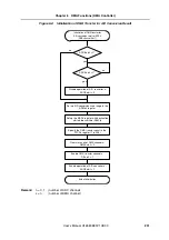
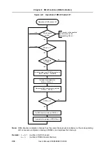
Page 209: ...Initialization of DMA transfer for serial data reception DMA channel 4 or 5 Set up MARx register with the destination start address in iRAM Specify the DMA transfer count in the DTCRx register 1 to 25...

Page 210: ...trigger factor occurred Transfer content from serial receive buffer depending on DTFRx register to iRAM MARx SIRBn or CBnRX Increment source pointer MARx MARx 2 Decrement DMA transfer count register...

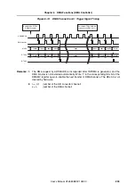
Page 211: ...Channel 4 and 5 Trigger Signal Timing Remark m 4 5 n 0 1 1000H 1002H 1004H 1006H 1008H 0003H 0002H 0001H 0000H 0000H 100CH 100EH 1010H 0002H 0001H 0000H 100AH 0003H MARm DTCRm DTRFm DMAMCm DTCRm DMAMC...

Page 212: ...bits transfer data size the source address must be even and is incremented by 2 for each DMA trigger When the DMA transfer count of a DMA channel terminates the DMA transfer is stopped and a DMA comp...

Page 213: ...nel Initialization of DMA transfer for serial data transmission DMA channel 6 or 7 Set up MARx register with the source start address in iRAM Specify the DMA transfer count in the DTCRx register 1 to...

Page 214: ...Channel 6 and 7 Trigger Signal Timing Remark m 6 7 n 0 1 1000H 1002H 1004H 1006H 1008H 0003H 0002H 0001H 0000H 0000H 100CH 100EH 1010H 0002H 0001H 0000H 100AH 0003H MARm DTCRm DTRFm DMAMCm DTCRm DMAMC...

Page 215: ...DMA trigger factor occurred Transfer content from iRAM to serial transmit buffer spec by DTFRx register SFDBn or CBnTX MARx Increment source pointer MARx MARx 2 Decrement DMA transfer count register D...

Page 216: ...rst after it has been finished see Figure 6 20 Figure 6 20 CPU and DMA Controller Processing of DMA Transfer Termination Example SAR2 0AH DTCR2 8 DMAS2 0 DE2 1 DMA transfer channel 2 enabled DMA trans...

Page 217: ...ge 219 Table 6 4 shows the relations between DMA trigger factors and DMA completion interrupts Notes 1 Not available on PD70F3447 2 An interrupt request is not generated for a signal which serves as D...

Page 218: ...interface Interrupt signals without quote mark are provided to the interrupt controller INTUC0R INTUC1R INTUC0R INTUC1R INTUC0R INTUC1R INTCB0R INTCB1R INTCSI30 INTCSI31 INTCB0R INTCB1R INTCB0R INTCB1...

Page 219: ...riority Mask can be specified to each maskable interrupt request Valid edge for detection of external interrupt request signal can be specified Exceptions Software exceptions 32 sources Exception trap...

Page 220: ...000001E0H nextPC Interrupt INTTR1OV PIC23 TR1CNT overflow TMR1 23 01F0H 000001F0H nextPC Interrupt INTTR1CC0 PIC24 TIR10 capture input TR1CCR0 match TMR1 24 0200H 00000200H nextPC Interrupt INTTR1CC1...

Page 221: ...TMP4 54 03E0H 000003E0H nextPC Interrupt INTP4CC1 PIC55 TIP41 capture input TP4CCR1 match TMP4 55 03F0H 000003F0H nextPC Interrupt INTP5OV PIC56 TMP5overflow TMP5 56 0400H 00000400H nextPC Interrupt...

Page 222: ...SIB1 reception completion DMA transfer completion CSIB1 Note DMAC 83 05B0H 000005B0H nextPC Interrupt INTCB1RE PIC84 Note CSIB1 receive error CSIB1 Note 84 05C0H 000005C0H nextPC Interrupt INTC30OVF P...

Page 223: ...illegal instruction when an illegal opcode exception occurs is calculated by Restored PC 4 Maskable Interrupt INTAD1 PIC96 ADC1 conversion completion DMA transfer completion ADC1 DMAC 96 0680H 0000068...

Page 224: ...of the interrupt mode register 0 INTM0 is detected at the NMI pin the interrupt occurs While the service program of the non maskable interrupt is being executed PSW NP 1 the acknowledgment of another...

Page 225: ...f ECR 4 Sets the NP and ID bits of the PSW and clears the EP bit 5 Sets the handler address 00000010H corresponding to the non maskable interrupt to the PC and transfers control The processing configu...

Page 226: ...equest is generated twice while a NMI service program is being executed Main routine NMI request NMI request PSW NP 1 NMI request held pending because PSW NP 1 Pending NMI request processed Main routi...

Page 227: ...is 1 2 Transfers control back to the address of the restored PC and PSW Figure 7 3 illustrates how the RETI instruction is processed Figure 7 3 RETI Instruction Processing Caution When the PSW EP bit...

Page 228: ...be specified by the interrupt mode register 0 INTM0 The valid edge of the external NMI pin input can be specified by the ESN0 and ESN1 bits The INTM0 register can be read written in 8 bit or 1 bit un...

Page 229: ...vicing of interrupts having a higher priority than the interrupt request in progress specified by the interrupt control register Note that only interrupts with a higher priority will have this capabil...

Page 230: ...SW ID 0 as set by the RETI and LDSR instructions input of the pending INT starts the new maskable interrupt processing INT input xxIF 1 No xxMK 0 No Is the interrupt mask released Yes Yes No No No Mas...

Page 231: ...ored PC and PSW Figure 7 7 illustrates the processing of the RETI instruction Figure 7 7 RETI Instruction Processing Note For the ISPR register see 7 3 6 In service priority register ISPR on page 242...

Page 232: ...ore interrupts having the same priority level specified by the PRn bit are generated at the same time interrupts are serviced in order depending on the priority level allocated to each interrupt reque...

Page 233: ...Main routine EI EI Interrupt request a level 3 Processing of a Processing of b Processing of c Interrupt request c level 3 Processing of d Processing of e EI Interrupt request e level 2 Processing of...

Page 234: ...evel 3 Interrupt request n level 1 Processing of o Interrupt request p level 2 Interrupt request q level 1 Interrupt request r level 0 Interrupt request u level 2 Note 2 Interrupt request t level 2 No...

Page 235: ...rrupt servicing restore the values of EIPC and EIPSW after executing the DI instruction Default priority a b c Main routine EI Interrupt request a level 2 Interrupt request b level 1 Interrupt request...

Page 236: ...wledged Remark n 0 to 105 see Table 7 2 Addresses and Bits of Interrupt Control Registers After reset 47H R W Address Refer to Table 7 2 7 6 5 4 3 2 1 0 PICn IFn MKn 0 0 0 PRn2 PRn1 PRn0 IFn Interrupt...

Page 237: ...17 0 0 0 PR172 PR171 PR170 INTTR0CC3 FFFFF134H PIC18 IF18 MK18 0 0 0 PR182 PR181 PR180 INTTR0CC4 FFFFF136H PIC19 IF19 MK19 0 0 0 PR192 PR191 PR190 INTTR0CC5 FFFFF138H PIC20 IF20 MK20 0 0 0 PR202 PR201...

Page 238: ...TP5CC0 FFFFF184H PIC58 IF58 MK58 0 0 0 PR582 PR581 PR580 INTP5CC1 FFFFF186H PIC59 IF59 MK59 0 0 0 PR592 PR591 PR590 INTP6OV FFFFF188H PIC60 IF60 MK60 0 0 0 PR602 PR601 PR600 INTP6CC0 FFFFF18AH PIC61 I...

Page 239: ...0 PR902 PR901 PR900 INTUC0R FFFFF1C6H PIC91 IF91 MK91 0 0 0 PR912 PR911 PR910 INTUC0T FFFFF1C8H PIC92 IF92 MK92 0 0 0 PR922 PR921 PR920 INTUC1RE FFFFF1CAH PIC93 IF93 MK93 0 0 0 PR932 PR931 PR930 INTUC...

Page 240: ...t as a reserved word If a bit is manipulated using the name of MKn the contents of the PICn register instead of the IMRm register are rewritten as a result the contents of the IMRm register are also r...

Page 241: ...W Address IMR4 FFFFF108H IMR4L FFFFF108H IMR4H FFFFF109H 15 14 13 12 11 10 9 8 IMR4 MK79 MK78 Note MK77 Note MK76 Note MK75 Note MK74 MK73 MK72 MK71 MK70 MK69 MK68 MK67 MK66 MK65 MK64 After reset FFFF...

Page 242: ...interrupt servicing or exception processing Reset input clears this register to 00H This register is read only in 8 bit or 1 bit units Caution In the interrupt enabled EI state if an interrupt is ack...

Page 243: ...truction or LDSR instruction when referencing the PSW Non maskable interrupt and exceptions are acknowledged regardless of this flag When a maskable interrupt is acknowledged the ID flag is automatica...

Page 244: ...skable external interrupt input pin INTPn can be selected by program n 0 to 12 The edge that can be selected as the valid edge is one of the following Rising edge Falling edge Both the rising and fall...

Page 245: ...he interrupt status flag after changing the bits ESn0 ESn1 of the interrupt channel n 0 to 2 After reset 00H R W Address FFFFF880H 7 6 5 4 3 2 1 0 INTM0 ES21 ES20 ES11 ES10 ES01 ES00 ESN1 ESN0 ES21 ES...

Page 246: ...e interrupt status flag after changing the bits ESn0 ESn1 of the interrupt channel n 3 to 6 After reset 00H R W Address FFFFF882H 7 6 5 4 3 2 1 0 INTM1 ES61 ES60 ES51 ES50 ES41 ES40 ES31 ES30 ES61 ES6...

Page 247: ...nterrupt status flag after changing the bits ESn0 ESn1 of the interrupt channel n 7 to 10 After reset 00H R W Address FFFFF884H 7 6 5 4 3 2 1 0 INTM1 ES101 ES100 ES91 ES90 ES81 ES80 ES71 ES70 ES101 ES...

Page 248: ...ESn1 may trigger an unintended interrupt event for the respective interrupt channels Be sure to mask the respective interrupt channel and clear the interrupt status flag after changing the bits ESn0...

Page 249: ...exception code to the lower 16 bits EICC of ECR interrupt source 4 Sets the EP and ID bits of PSW 5 Loads the handler address 00000040H or 00000050H of the software exception routine in the PC and tra...

Page 250: ...l to the address of the restored PC and PSW The processing of the RETI instruction is shown below Figure 7 20 RETI Instruction Processing Caution When the PSW EP bit and the PSW NP bit are changed by...

Page 251: ...lag used to indicate that exception processing is in progress This flag is set when an exception occurs Figure 7 21 Exception Status Flag EP 31 8 7 6 5 4 3 2 1 0 After reset 00000020H PSW 0 0 0 0 0 0...

Page 252: ...instruction applicable to this illegal instruction is executed Figure 7 22 Illegal Opcode Caution Caution Since it is possible that this instruction may be assigned to an illegal opcode in the future...

Page 253: ...nd controls the address of the restored PC 1 Loads the restored PC and PSW from DBPC and DBPSW 2 Transfers control to the address indicated by the restored PC and PSW Figure 7 24 illustrates the resto...

Page 254: ...e next instruction interrupt is held pending The interrupt request non sample instructions are as follows EI instruction DI instruction LDSR reg2 0x5 instruction for PSW The store instruction for the...

Page 255: ...mark fX External resonator or external clock frequency fXX Internal system clock An external resonator or crystal is connected to X1 and X2 pins whose frequency is multiplied by the PLL synthesizer By...

Page 256: ...ved due to a combination of HALT mode and normal operation mode The system is switched to HALT mode by a specific instruction the HALT instruction Figure 8 2 shows the operation of the clock generator...

Page 257: ...power consumption of the system can be reduced by using the HALT mode in combination with the normal operation mode for intermittent operation Cautions 1 Insert five or more NOP instructions after the...

Page 258: ...than or same as the interrupt currently being serviced is generated the HALT mode is released but the newly generated interrupt request signal is not acknowledged The interrupt request signal itself...

Page 259: ...operations PWM output Interval timer External event counter operation not possible when clock is stopped One shot pulse output Pulse width measurement 9 2 Function Outline Capture trigger input signal...

Page 260: ...ion Timer register 16 bit counter Registers TMPn capture compare registers 0 1 TPnCCR0 TPnCCR1 TMPn counter register TPnCNT CCR0 buffer register CCR1 buffer register Timer input 2 8 TIPm0 TIPm1 TTRGPm...

Page 261: ...a Use as compare register TPnCCR0 can be rewritten when TPnCE 1 The timing at which the TPnCCR0 rewrite values become valid when TPnCE 1 is as follows b Use as capture register TMP0 to TMP7 The count...

Page 262: ...a Use as compare register TPnCCR1 can be rewritten when TPnCE 1 The timing at which the TPnCCR1 rewrite values become valid when TPnCE 1 is as follows b Use as capture register TMP0 to TMP7 The counte...

Page 263: ...t is cleared to 0 Figure 9 4 TMPn Counter Register TPnCNT Remark The value of the TPnCNT register is cleared to 0000H when the TPnCE bit 0 If the TPnCNT register is read at this time the value of the...

Page 264: ...FFFFF620H TP3CTL0 FFFFF630H TP4CTL0 FFFFF640H TP5CTL0 FFFFF650H TP6CTL0 FFFFF660H TP7CTL0 FFFFF670H TP8CTL0 FFFFF680H 7 6 5 4 3 2 1 0 TPnCTL0 TPnCE 0 0 0 0 TPnCKS2 TPnCKS1 TPnCKS0 n 0 to 8 TPnCE Timer...

Page 265: ...Mode Selection 0 Timer Pn operates in single operation mode 1 Timer Pn operates in synchronous operation modeNote This bit supports synchronous operation of two or more timer P Two groups of timers ex...

Page 266: ...nal clock selected by bits TPnCKS2 to TPnCKS0 1 Use external clock input TEVTPn input edge Note When TPnEEE 1 external clock input TEVTPn the valid edge is specified by bits TPnEES1 and TPnEES0 Note E...

Page 267: ...C0 FFFFF612H TP2IOC0 FFFFF622H TP3IOC0 FFFFF632H TP4IOC0 FFFFF642H TP5IOC0 FFFFF652H TP6IOC0 FFFFF662H TP7IOC0 FFFFF672H TP8IOC0 FFFFF682H 7 6 5 4 3 2 1 0 TPnIOC0 0 0 0 0 TPnOL1 TPnOE1 TPnOL0 TPnOE0 n...

Page 268: ...can be written when TPnCE 1 If rewriting was mistakenly performed set TPnCE 0 and then set the bits again 2 The TPnIS3 to TPnIS0 bits are valid only in the free running mode and the pulse width measu...

Page 269: ...PnEES0 bits are valid only when TPnEEE 1 or when the external event count mode TPnMD2 to TPnMD0 001B of the TPnCTL1 register has been set Remark n 0 to 7 After reset 00H R W Address TP0IOC2 FFFFF604H...

Page 270: ...CCR1 register capture compare selection 0 Compare register selection 1 Capture register selection The TPnCCS1 bit settings are valid only in the free running mode TPnCCS0 TPnCCR0 register capture comp...

Page 271: ...FFF6F0H 7 6 5 4 3 2 1 0 TPIC0 0 0 0 0 TPIC03 TPIC02 TPIC01 TPIC00 TPIC03 TP3CCR1 Register Capture Source Input Selection 0 Capture source input is pin P17 TIP31 1 Capture source input is pin P16 TIP30...

Page 272: ...le After reset 00H R W Address FFFFF6F2H 7 6 5 4 3 2 1 0 TPIC1 0 0 TIP15 TIP14 TPIC13 TPIC12 TPIC11 TPIC10 TPIC15 Note TIPC14 TIPC13 Capture Source Input Selection of TP7CCR0 TP7CCR1 0 0 0 Pin P26 TIP...

Page 273: ...egister 1 TPIC1 Note Setting TIPC22 to 1 is prohibited for PD70F3447 since TMENC1 is not available After reset 00H R W Address FFFFF6F4H 7 6 5 4 3 2 1 0 TPIC2 0 0 0 0 0 TPIC22 TPIC21 TPIC20 TIPC22 Not...

Page 274: ...n TPnCE 1 but the write method anytime rewrite reload differs depending on the mode 1 Anytime rewrite When the TPnCCRm register is written during timer operation the write data is transferred at that...

Page 275: ...operation in the interval timer mode 2 n 0 to 8 START Initial settings INTTPnCC0 output TPnCCR1 rewrite Transfer to CCR1 buffer register TPnCCR0 rewrite Transfer to CCR0 buffer register Match between...

Page 276: ...0 register 0000H to FFFFH D11 D12 Setting values of TPnCCR1 register 0000H to FFFFH 2 The above timing chart illustrates an example of the operation in the interval timer mode 3 n 0 to 8 16 bit counte...

Page 277: ...Thereafter the values of the TPnCCR0 and the TPnCCR1 register are reloaded upon TPnCCR0 register match Whether to enable or disable the next reload timing is controlled by writing to the TPnCCR1 regis...

Page 278: ...value of TPnCCR0 register 0000H to FFFFH D11 D12 Setting value of TPnCCR1 register 0000H to FFFFH 2 The above timing chart illustrates the operation in the PWM mode as an example 3 n 0 to 8 D01 D01 D...

Page 279: ...the setting value of the TPnCCR1 register is transferred to the CCR1 buffer register and compared with the value of the 16 bit counter and an interrupt request INTTPnCC1 is output if these values mat...

Page 280: ...ote The 16 bit counter is not cleared when its value matches the value of TPnCCR1 Remarks 1 D1 D2 Setting values of TPnCCR0 register 0000H to FFFFH D3 Setting value of TPnCCR1 register 0000H to FFFFH...

Page 281: ...tput TPnOE0 TPnOE1 1 TPnOL0 0 TPnOL1 1 Remarks 1 D1 Setting value of TPnCCR0 register 0000H to FFFFH D2 Setting value of TPnCCR1 register 0000H to FFFFH 2 Interval time tDn Dn 1 count clock cycle 3 n...

Page 282: ...and the value of the CCR0 buffer register 16 bit counter clearing using the TPnCCR1 register is not performed However the setting value of the TPnCCR1 register is transferred to the CCR1 buffer regist...

Page 283: ...register Remark n 0 to 7 START Initial settings External event count mode setting TPnCTL0 TPnMD2 to TPnMD0 001 Note 1 Valid edge setting TPnIOC2 TPnEES1 TPnEES0 Compare register setting TPnCCR0 TPnCCR...

Page 284: ...2 D3 rewrite of TPnCCR0 only no TOPn1 output Remarks 1 D1 D2 Setting values of TPnCCR0 register 0000H to FFFFH D3 Setting value of TPnCCR1 register 0000H to FFFFH 2 Event count Dn 1 3 n 0 to 7 16 bit...

Page 285: ...1 D2 no TPnCCR0 TPnCCR1 rewrite TOPn1 output Remarks 1 D1 Setting value of TPnCCR0 register 0000H to FFFFH D2 Setting value of TPnCCR1 register 0000H to FFFFH 2 Event count Dn 1 3 n 0 to 7 16 bit coun...

Page 286: ...ming is controlled by writing to the TPnCCR1 register Thus even when wishing only to rewrite the value of the TPnCCR0 register also write the same value to the TPnCCR1 register Reload is disabled even...

Page 287: ...PnEEE 0 TPnCTL0 TPnCKS2 to TPnCKS0 External trigger pulse output mode setting TPnCTL1 TPnMD2 to TPnMD0 010 Compare register setting TPnCCR0 TPnCCR1 Match between 16 bit counter and TPnCCR1Note INTTPnC...

Page 288: ...2 Setting value of TPnCCR1 register 0000H to FFFFH 2 TOPn1 output duty Setting value of TPnCCR1 register Setting value of TP0CCR0 register TOPn1 output cycle Setting value of TPnCCR0 register Count cl...

Page 289: ...when the 16 bit counter has stopped at 0000H In the one shot pulse mode the TPnCCR0 and TPnCCR1 registers can be rewritten when TPnCE 1 The setting values rewritten to the TPnCCR0 and TPnCCR1 registe...

Page 290: ...r Remark n 0 to 8 START Initial settings Clock selection TPnCTL1 TPnEEE 0 TPnCTL0 TPnCKS2 to TPnCKS0 One shot pulse mode setting TPnCTL1 TPnMD2 to TPnMD0 011B Compare register setting TPnCCR0 TPnCCR1...

Page 291: ...ilable for TMP8 n 8 Remarks 1 D0 Setting value of TPnCCR0 register 0000H to FFFFH D1 Setting value of TPnCCR1 register 0000H to FFFFH 2 Delay time of one shot pulse output TOPn1 when external pin edge...

Page 292: ...then write to the TPnCCR1 register before the 16 bit counter value and the TPnCCR0 register value match Thereafter the values of the TPnCCR0 register and the TPnCCR1 register are reloaded upon a TPnCC...

Page 293: ...tings Clock selection TPnCTL0 TPnCKS2 to TPnCKS0 PWM mode settings TPnCTL1 TPnMD2 to TPnMD0 100B Compare register setting TPnCCR0 TPnCCR1 Match between 16 bit counter and CCR1 buffer register TOPn1 lo...

Page 294: ...mode setting TPnCTL1 TPnMD2 to TPnMD0 100B Compare register setting TPnCCR0 TPnCCR1 Match between 16 bit counter and TPnCCR1 TOPn1 low level output Match between 16 bit counter and TPnCCR0 16 bit cou...

Page 295: ...alues of TPnCCR1 register 0000H to FFFFH 2 TOPn1 output duty factor Setting value of TPnCCR1 register Setting value of TP0CCR0 register 1 TOPn1 output cycle Setting value of TPnCCR0 register 1 Count c...

Page 296: ...0 D11 D12 D13 Setting values of TPnCCR1 register 0000H to FFFFH 2 TOPn1 output duty factor Setting value of TPnCCR1 register Setting value of TP0CCR0 register 1 TOPn1 output cycle Setting value of TPn...

Page 297: ...rupt is output upon a match between the 16 bit counter and the CCR1 buffer register in the free running mode interval function Rewrite during compare timer operation is enabled and performed with anyt...

Page 298: ...of the 16 bit counter is saved to the TPnCCR0 register upon TIPn0 pinNote 1 edge detection Notes 1 Since TMP8 has no external input pin the capture function can only be used internally for capturing t...

Page 299: ...of TPnCCR1 value to CCR1 buffer register TIPn1 edge detection capture of 16 bit counter value to TPnCCR1 TIPn0 edge detection capture of 16 bit counter value to TPnCCR0 16 bit counter overflow Timer o...

Page 300: ...e trigger is input Moreover when TPnOEm 1 is set TOPnm performs toggle output upon a match between the 16 bit counter and the CCRm buffer register Figure 9 29 Basic Operation Timing in Free Running Mo...

Page 301: ...ing the overflow flag TPnOVF However if overflow occurs twice 2 or more free running cycles the capture trigger interval cannot be judged with the TPnOVF flag In this case the system should be revised...

Page 302: ...e TPnCCR0 register as an interval function Even if TPnOE1 1 is set to realize the capture function the TPnCCR1 register cannot control TOPn1 Figure 9 31 Basic Operation Timing in Free Running Mode TPn...

Page 303: ...2 Basic Operation Timing in Free Running Mode TPnCCS1 0 TPnCCS0 1 Remarks 1 D00 D01 D02 D03 Values captured to TPnCCR0 register 0000H to FFFFH D10 D11 D12 Setting value of TPnCCR1 register 0000H to FF...

Page 304: ...lected capture input sources and specified edge detection three different measurement methods can be applied 1 Pulse period measurement 2 Alternating pulse width and pulse space measurement This requi...

Page 305: ...nting Figure 9 33 Flowchart of Pulse Period Measurement Note External pulse input is possible for both TIPn0 and TIPn1 but only one should be selected for the pulse period measurement Specify either r...

Page 306: ...ent Remarks 1 D00 D01 D02 Values captured to TPnCCR0 register 0000H to FFFFH 2 TIPn0 Set to detection of rising edge TPnIS1 TPnIS0 01B 3 TIPn1 Set to no edge detection TPnIS3 TPnIS2 00B 4 n 0 to 7 D00...

Page 307: ...hart of Alternating Pulse Width and Pulse Space Measurement Note External pulse input is possible for both TIPn0 and TIPn1 but only one should be selected for the alternating pulse width and pulse spa...

Page 308: ...rks 1 D00 D01 D02 D03 D04 Values captured to TPnCCR0 register 0000H to FFFFH 2 TIPn0 Set to detection of both rising and falling edges TPnIS1 TPnIS0 11B 3 TIPn1 Set to no edge detection TPnIS3 TPnIS2...

Page 309: ...sters TPnCCR0 TPnCCR1 and the timer is cleared and restarts counting Figure 9 37 Flowchart of Simultaneous Pulse Width and Pulse Space Measurement Note External pulse input must be input to both TIPn0...

Page 310: ...ut on TIPn0 pin In case of internal connection the signal has to be input on TIPn0 pin Remarks 1 D00 D01 D02 Values captured to TPnCCR0 register 0000H to FFFFH 2 D10 D11 Values captured to TPnCCR1 reg...

Page 311: ...1 Clear the synchronous mode selection bit TPmSYE of the master counter TMPm to 0 2 Disable the count operation of the master counter TMPm TPmCE 0 3 Enable the synchronous operation for each of the i...

Page 312: ...312 Chapter 9 16 Bit Timer Event Counter P User s Manual U16580EE3V1UD00 MEMO...

Page 313: ...stop function ESO High impedance output of pins TORn0 to TORn7 possible during ESOn input Compare value setting Reload batch rewrite anytime rewrite mode selectable Note Reload mode Reload enabled by...

Page 314: ...ompare registers 0 to 3 TRnCCR0 TRnCCR3 Timer Rn compare registers 4 5 TRnCCR4 TRnCCR5 TRnCCR0 to TRnCCR5 buffer registers TRnDTC0 TRnDTC1 buffer registers Timer input pins 3 TIR10 to TIR13 TTRGR1 TEV...

Page 315: ...uffer CCR5 buffer TRnSBC TRnCNT TRnCUF TRnCUF TRnADTRG0 TORn0 TIR10 TTRGR1 TEVTR1 TIR11 TIR12 TIR13 TORn1 TORn2 TORn3 TORn4 TORn5 TORn6 TORn7 TRnADTRG1 INTTRnO V INTTRnOD INTTRnCD INTTRnCC0 INTTRnCC1...

Page 316: ...a Use as compare register When TRnCE 1 the TRnCCR0 register write access method is as follows Remarks 1 For details about the compare register rewrite operation refer to 10 4 2 Compare register rewri...

Page 317: ...in 16 bit units RESET input clears this register to 0000H Remarks 1 In the high accuracy T PWM mode when bit 0 is set to 1 the additional pulse control function is engaged For details about the addit...

Page 318: ...o 1 the additional pulse control function is engaged For details about the additional pulse control function refer to 10 10 9 10 10 9 2 n 0 1 Figure 10 4 TMRn Capture Compare Register 2 TRnCCR2 a Use...

Page 319: ...to 1 the additional pulse control function is engaged For details about the additional pulse control function refer to 10 10 9 10 10 9 2 n 0 1 Figure 10 5 TMRn Capture Compare Register 3 TRnCCR3 a Use...

Page 320: ...mode bit 0 of the TRnCCR4 register is ignored 2 n 0 1 Figure 10 6 TMRn Compare Register 4 TRnCCR4 When TRnCE 1 the TRnCCR4 register write access method is as follows Remarks 1 For details about the co...

Page 321: ...he TRnCCR5 register is ignored 2 n 0 1 Figure 10 7 TMRn Compare Register 5 TRnCCR5 When TRnCE 1 the TRnCCR5 register write access method is as follows Remarks 1 For details about the compare register...

Page 322: ...de bit 0 is read as 0 Remark n 0 1 8 TMRn sub counter read register TRnSBC The TRnSBC register can read the value of the 16 bit counter This register can only be read in 16 bit units RESET input or se...

Page 323: ...r 0 TRnDTC0 10 TMRn dead time setting register 1 TRnDTC1 The TRnDTC1 register is a 10 bit register that specifies the dead time value This register can be read and written in 16 bit units Reset input...

Page 324: ...g clock operation disabled Reset timer Rn asynchronously 1 Internal operating clock operation enabled When bit TRnCE is set to 0 the internal operation clock of timer Rn stops fixed to low level and t...

Page 325: ...fXX 8 0 1 1 fXX 16 1 0 0 fXX 32 1 0 1 fXX 64 1 1 0 fXX 256 1 1 1 fXX 1024 Caution Set bits TRnCKS2 to TRnCKS0 when TRnCE 0 When bit TRnCE is set from 0 to 1 bits TRnCKS2 to TRnCKS0 can be simultaneous...

Page 326: ...ess TR0CTL1 FFFFF581H TR1CTL1 FFFFF5C1H 7 6 5 4 3 2 1 0 TRnCTL1 0 TRnEST TRnEEE 0 TRnMD3 TRnMD2 TRnMD1 TRnMD0 n 0 1 TRnEST Software Trigger Control 0 No operation 1 Enables software trigger control In...

Page 327: ...ent count mode Note 1 0 0 1 0 External trigger pulse output mode Note 2 0 0 1 1 One shot pulse mode 0 1 0 0 PWM mode 0 1 0 1 Free running mode 0 1 1 0 Pulse width measurement mode Note 1 0 1 1 1 Trian...

Page 328: ...may occur on the output pin set the TRnIOC0 register when TRnCE 0 When TRnCE 1 the TRnIOC0 register can be write accessed using the same value Figure 10 14 TMRn I O Control Register 0 TRnIOC0 Remark...

Page 329: ...R W Address FFFFF5C3H 7 6 5 4 3 2 1 0 TR1IOC1 TR1IS7 TR1IS6 TR1IS5 TR1IS4 TR1IS3 TR1IS2 TR1IS1 TR1IS0 TR1IS7 TR1IS6 Capture Input TIR13 Valid Edge Setting 0 0 No edge detection capture operation inval...

Page 330: ...0 0 0 0 TR1EES1 TR1EES0 TR1ETS1 TR1ETS0 TR1EES1 TR1EES0 External Event Counter Input TEVTR1 Valid Edge Setting 0 0 No edge detection capture operation invalid 0 1 Rising edge detection 1 0 Falling ed...

Page 331: ...ay occur on the output pin set the TRnIOC3 register when TRnCE 0 When TRnCE 1 the TRnIOC0 register can be write accessed using the same value Figure 10 17 TMRn I O Control Register 3 TRnIOC3 Remark n...

Page 332: ...TORn5 and TORn6 Remark If simultaneous active state is detected when TRnTBA2 1 the TRnTBF flag is set 1 and an error interrupt INTTRnER is output TRnTBA1 Timer Outputs TORn3 TORn4 True Bar Active Det...

Page 333: ...0 TR1CMS TR1CUF TR1OVF TR1CCS3 TR1CCR3 register capture compare selection 0 Select compare register 1 Select capture register Remark Bit TR1CCS3 is only valid in the free running mode In all other mod...

Page 334: ...RnCUF Timer R Counter Up Down Detection Flag 0 The timer counter is in up count state 1 The timer counter is in down count state Remark The TRnCUF bit is valid only in the high accuracy T PWM mode and...

Page 335: ...H TR1OPT1 FFFFF5CEH 7 6 5 4 3 2 1 0 TRnOPT1 TRnICE TRnIOE TRnRDE TRnID4 TRnID3 TRnID2 TRnID1 TRnID0 n 0 1 TRnICE Peak Interrupts INTTRnCD Control 0 Disable peak interrupt INTTRnCD output in the counte...

Page 336: ...lid only in the PWM mode high accuracy T PWM mode triangular wave PWM output mode and PWM mode with dead time TRnID4 TRnID3 TRnID2 TRnID1 TRnID0 Interrupt Thinning Out Rate 0 0 0 0 0 No thinning out 0...

Page 337: ...angular wave PWM mode when setting TRnAT02 1 set TRnOE4 0 Figure 10 21 TMRn Option Register 2 TRnOPT2 1 2 Remark n 0 1 After reset 00H R W Address TR0OPT2 FFFFF588H TR1OPT2 FFFFF5C8H 7 6 5 4 3 2 1 0 T...

Page 338: ...verter Trigger Signal TRnADTRG0 Generation with Occurrence of Peak Interrupt INTTRnCD 0 No trigger signal is generated when peak interrupt INTTRnCD occurs 1 Trigger signal is generated when peak inter...

Page 339: ...gular wave PWM mode when setting TRnAT12 1 set TRnOE4 0 Figure 10 22 TMRn Option Register 3 TRnOPT3 1 2 Remark n 0 1 After reset 00H R W Address TR0OPT3 FFFFF589H TR1OPT3 FFFFF5C9H 7 6 5 4 3 2 1 0 TRn...

Page 340: ...Converter Trigger Signal TRnADTRG1 Generation with Occurrence of Peak Interrupt INTTRnCD 0 No trigger signal is generated when peak interrupt INTTRnCD occurs 1 Trigger signal is generated when peak i...

Page 341: ...Remarks 1 The TRnTBF flag is set 1 upon detection that any of the normal phases TORn1 TORn3 TORn5 and inverted phases TORn2 TORn4 TORn6 are simultaneously active and an error interrupt INTTRnER is out...

Page 342: ...Remark n 0 1 After reset 00H R W Address TR0OPT7 FFFFF58DH TR1OPT7 FFFFF5CDH 7 6 5 4 3 2 1 0 TRnOPT7 0 0 0 0 0 0 0 TRnTOS n 0 1 TRnTOS Timer Output TORn0 Switching Control 0 Output counter s TRnCNT up...

Page 343: ...r and the compare register Counting immediately following the start of count operation and counting from FFFFH to 0000H in the case of overflow are not detected as clear operations 3 Overflow operatio...

Page 344: ...RnCC3 Functions as TRnCCRn3 buffer register match interrupt INTTRnCC4 Functions as TRnCCRn4 buffer register match interrupt INTTRnCC5 Functions as TRnCCRn5 buffer register match interrupt INTTRnCD Fun...

Page 345: ...written to the register is updated to the value written during anytime write access Reload mode batch rewrite When the TRnCCR1 register is written to all the registers are updated at the next reload...

Page 346: ...nterrupt 2 Set with TRnOPT0 register bit TRnCMS 0 TRnOPT1 register bit TRnRDE 0 Mode Rewrite Timing Interval mode Anytime rewrite External event count mode Anytime rewrite External trigger pulse outpu...

Page 347: ...e only the TRnCCR1 register has a 2 stage configuration the actual transfer timing is after the lapse of 5 clocks fTMRn Figure 10 25 Anytime Rewrite Timing Remarks 1 D01 D02 TRnCCR0 register setting v...

Page 348: ...erred to the TRnCCR0 buffer register at the next peak or at the valley timing Since TRnCMS 1 anytime rewrite the settings of bits TRnIOE TRnICE TRnRDE and TRnID4 to TRnID0 have no influence b Cautions...

Page 349: ...ch occurrence In the case of rewrite after a match between the TRnCCR1 to TRnCCR3 registers and the counter occurs further match occurrences are ignored so the rewrite value is not reflected Counter T...

Page 350: ...rewrite and the rewrite value is instantly reflected If a value larger than the counter value is written before match occurrence no match occurs so the following output wave results If no match occurs...

Page 351: ...ewriting TRnOPT1 Since the internal interrupt thinning out counter is cleared when the TRnOPT1 register is written to the interrupt output interval may temporarily become longer Counter TRnCCR1 i k TR...

Page 352: ...0 26 Basic Operation Flow during Batch Rewrite Caution Write access to the TRnCCR1 register includes also the reload enable operation Therefore rewrite the TRnCCR1 register after rewriting the other T...

Page 353: ...TRnCCR0 buffer TRnCCR1 TRnCCR1 buffer TRnCCR2 TRnCCR2 buffer TRnCCR3 TRnCCR3 buffer TRnCCR4 TRnCCR4 buffer TRnCCR5 TRnCCR5 buffer TRnOPT1 TRnOPT1 buffer Reload rewrite timing Counter INTTRnOD INTTRnCD...

Page 354: ...ng 2 2 Counter Reload upon TRnCCR1 write Batch update at reload timing Setting of reload hold flag Flag clearing following reload TRnCCR0 TSnCCR0 buffer TRnCCR1 TSnCCR1 buffer TRnCCR2 TSnCCR2 buffer T...

Page 355: ...TRnICE 1 TRnIOE 1 settings Rewrite in 1 interval rewrite during up count Since the next reload timing becomes the peak point the cycle on the down count side changes and an asymmetrical triangular wav...

Page 356: ...unt Since the next reload timing becomes the valley point the cycle value changes from the next cycle and the asymmetrical triangular waveform output is held Since the cycle changes be sure to set aga...

Page 357: ...ite in 1 interval rewrite during up count Since reload is performed at the peak interrupt timing an asymmetric triangular waveform is output Rewrite in 2 interval rewrite during down count Since reloa...

Page 358: ...e upon TRnCCR1 match Inactive upon TRnCCR0 match Active upon TRnCCR2 match Inactive upon TRnCCR0 match Active upon TRnCCR3 match Inactive upon TRnCCR0 match PWM mode Toggle output upon TRnCCR0 compare...

Page 359: ...h upon TRnCCR5 match Inactive upon TRnCCR0 match PWM mode PWM output upon TRnCCR4 compare match PWM output upon TRnCCR5 compare match Pulse output upon A D conversion trigger Note Free running mode To...

Page 360: ...1 its set 1 status is maintained If the TRnADTRG1 trigger occurs while pin TORn7 is reset 0 the 0 status is maintained If the TRnADTRG0 and TRnADTRG1 signal triggers occur simultaneously pin TORn7 is...

Page 361: ...l trigger pulse output mode TRnCCR0 compare match interrupt TRnCCR1 compare match interrupt TRnCCR2 compare match interrupt TRnCCR3 compare match interrupt One shot pulse mode TRnCCR0 compare match in...

Page 362: ...TRnCCR4 compare match interrupt TRnCCR5 compare match interrupt External trigger pulse output mode TRnCCR4 compare match interrupt TRnCCR5 compare match interrupt One shot pulse mode TRnCCR4 compare m...

Page 363: ...ode PWM mode Select from interrupts INTTRnCD INTTRnCC4 INTTRnCC5 Select from interrupts INTTRnCD INTTRnCC4 INTTRnCC5 Peak interrupt at same timing as INTTRnCC0 interrupt Free running mode Pulse width...

Page 364: ...time If the counter is a triangular wave operation mode triangular wave PWM mode high accuracy PWM mode a peak interrupt is output when the counter switches from up count to down count If the counter...

Page 365: ...er s Manual U16580EE3V1UD00 Figure 10 29 Interrupt Signal Output Example 2 2 p FFFFH 0H TRnCCR0 TRnCCR1 TRnCCR2 TRnCCR3 p i j k p Counter INTTRnCD0 peak interrupt INTTRnOD valley interrupt INTTRnCC1 I...

Page 366: ...curacy T PWM mode if set in the range of 0000H TRnCCRm TRnDTC0 TRnCCR0 TRnDTC1 TRnCCRm TRnCCR0 no interrupt occurs upon a match between the compare value and the counter Remark m 1 to 3 Restrictions r...

Page 367: ...conditions no compare interrupt is output Restrictions related to TRnCCRm In the PWM mode with dead time if setting is performed in the following range no match between the compare value and counter o...

Page 368: ...is fixed to 0 in all other modes For both TRnCUF and TRnSUF 0 indicates the up count status and 1 indicates the down count status Figure 10 30 Up Count Flags Timings 1 2 In the triangular wave PWM mod...

Page 369: ...WM mode triangular wave PWM mode high accuracy T PWM mode and PWM mode with dead time Figure 10 31 Normal Phase Inverted Phase Simultaneous Active Detection Flag Timing TRnCUF TORn0 TRnSUF TORn0 TSnCC...

Page 370: ...is cleared to 0 The TRnRSF flag is valid in the following operation modes External trigger pulse output mode PWM mode Triangular wave PWM mode High accuracy T PWM mode TRnCMS 0 PWM mode with dead tim...

Page 371: ...interrupt output following thinning out If thinning out No is specified reload is executed at the reload timing after write access to the TRnCCR1 register The reload anytime rewrite method can be spe...

Page 372: ...g Out Operations 1 2 a when TRnICE 1 TRnIOE 1 peak valley interrupt output TRnID4 0 00H no th inning out TRnID4 0 01H mask 1 TRnID4 0 02H mask 2 TRnID4 0 03H mask 3 TRnID4 0 04H mask 4 TRnID4 0 05H ma...

Page 373: ...ly output Counter TRnID4 0 00H no th inning out INTTRnCD INTTRnOD TRnID4 0 01H mask 1 INTTRnCD INTTRnOD TRnID4 0 02H mask 2 INTTRnCD INTTRnOD TRnID4 0 03H mask 3 INTTRnCD INTTRnOD TRnID4 0 04H mask 4...

Page 374: ...TRnCMS 0 TRnRDE 1 Reload Thinning Out Control Recommended Settings b when TRnCMS 0 TRnRDE 0 No Reload Control Counter INTTRnCD INTTRnOD TRnIDS4 to 0 TRnID4 to 0 Reload Clear Interrupt thinning out cou...

Page 375: ...used to specify reload thinning out Yes No If thinning out Yes is specified reload is executed at the same timing as interrupt output following thinning out If thinning out No is specified reload is e...

Page 376: ...triggers peak inter rupts and valley interrupts in each mode Figure 10 35 A D Conversion Trigger Output Controller The above figure shows the A D conversion trigger controller As shown in this figure...

Page 377: ...nversion trigger outputtable upon compare match interrupt INTTRnCC4 during counter down count TRnOPT2 register TRnAT04 1 A D conversion trigger outputtable upon compare match interrupt INTTRnCC5 durin...

Page 378: ...When TRnAT05 to 00 000010 Output INTTRnCD When TRnAT05 to 00 000100 Output INTTRnCC4 during up count When TRnAT05 to 00 001000 Output INTTRnCC4 during down count When TRnAT05 to 00 010000 Output INTTR...

Page 379: ...2 Cautions related to A D conversion triggers In the PWM mode and PWM mode with dead time no valley interrupt INTTRnOD is output Only peak interrupts INTTRnCD are valid Counter INTTRnCD INTTRnOD When...

Page 380: ...ng bits TRnTBA2 to TRnTBA0 of the TRnIOC4 register The possibility of normal phase inverted phase simultaneous active error detection in each mode is indicated below Remark Error detection possible Er...

Page 381: ...re set so that pins TORn3 and TORn4 simultaneously output H Figure 10 38 Error Interrupt and Error Signal Output Controller in PWM mode If the output active level is switched by manipulating TRnIOC0 r...

Page 382: ...RnER is output when the TRnCCR0 and TRnCCR1 registers are set so that pins TORn1 and TORn2 simultaneously output H Similarly an error interrupt INTTRnER is output when the TRnCCR3 and TRnCCR4 register...

Page 383: ...rror occurs this is likely due to an internal circuit fault Figure 10 40 Error Interrupt and Error Signal Output Controller in High Accuracy T PWM Mode PWM Mode with Dead Time TORn1 TORn2 INTTRnER TRn...

Page 384: ...alues transferred to the TRnCCR1 to TRnCCR5 buffer registers and compare match interrupts INTTRnCC1 to INTTRnCCR5 are output The TRnCCR0 to TRnCCR5 registers can be rewritten using the anytime write m...

Page 385: ...pts Register Rewrite Method Rewrite during Operation Function TRnCCR0 Reload Possible Compare value TRnCCR1 to TRnCCR3 Reload Possible Compare value TRnCCR4 TRnCCR5 Reload Possible Compare value Pin F...

Page 386: ...ORn1 are not output TRnOE0 1 0 TRnOL0 0 TRnOL1 1 Remarks 1 D1 D2 Setting values of TRnCCR0 register 0000H to FFFFH D3 Setting values of TRnCCR1 register 0000H to FFFFH 2 Interval time Dm 1 count clock...

Page 387: ...Rn1 output performed TRnOE0 1 1 TRnOL0 0 TRnOL1 1 Remarks 1 D1 Setting value of TRnCCR0 register 0000H to FFFFH D2 Setting value of TRnCCR1 register 0000H to FFFFH 2 Interval time Dm 1 count clock cyc...

Page 388: ...OE1 to TRnOE7 are set to 1 When a compare register TRnCCR0 to TRnCCR5 is not used it is recommended to set it contents to FFFFH External event count operation flow 1 TRnCTL1 register bits TRnMD3 to TR...

Page 389: ...ite during Operation Function TRnCCR0 Anytime rewrite Possible Compare value TRnCCR1 to TRnCCR3 Anytime rewrite Possible Compare value TRnCCR4 TRnCCR5 Anytime rewrite Possible Compare value Pin Functi...

Page 390: ...nd TORn1 are not output The signal input from TEVTRn and internally synchronized is counted as the count clock TRnOE0 1 0 TRnOL0 0 TRnOL1 1 Remarks 1 D1 D2 Setting values of TRnCCR0 register 0000H to...

Page 391: ...CR0 and TRnCCR1 register values are not rewritten TORn0 and TORn1 are output TRnOE0 1 1 TRnOL0 0 TRnOL1 1 Remarks 1 D1 Setting value of TRnCCR0 register 0000H to FFFFH D2 Setting value of TRnCCR1 regi...

Page 392: ...When D1 D2 TRnCCR0 and TRnCCR1 register values are not rewritten TORn0 and TORn1 are output TRnOE0 1 1 TRnOL0 0 TRnOL1 1 Remarks 1 D1 Setting value of TRnCCR0 register 0000H D2 Setting value of TRnCC...

Page 393: ...d When D1 D2 TRnCCR0 TRnCCR1 register values are not rewritten TORn0 and TORn1 are output TRnOE0 1 1 TRnOL0 0 TRnOL1 1 Remarks 1 D1 Setting value of TRnCCR0 register 0001H D2 Setting value of TRnCCR1...

Page 394: ...be rewritten during count operation Compare register reload is performed at the timing when the counter value and the TR1CCR0 register match However when write access to the TR1CCR1 register is perfo...

Page 395: ...Cycle TR1CCR1 to TR1CCR3 Reload Possible Duty TR1CCR4 TR1CCR5 Reload Possible Duty Pin Function TIR1m m 0 to 3 TTRGR1 Counter clear start through external trigger input TEVTR1 Timer count through exte...

Page 396: ...l trigger TTRGR1 pin input Counter starts counting Counter clear start Initial settings Timer operation enable TR1CE 1 Transfer of valu es of TR1CCR0 to TR1CCR5 to buffers TR1CCR0 to TR1CCR5 Match bet...

Page 397: ...ister 0000H to FFFFH D11 D12 Setting values of TR1CCR1 register 0000H to FFFFH 2 TOR11 PWM duty setting value of TR1CCR1 register count clock cycle TOR11 PWM cycle setting value of TR1CCR0 register 1...

Page 398: ...t INTTRnCC0 is output and upon a match between the counter and TRnCCR1 to TRnCCR5 buffer registers compare match interrupts INTTRnCC1 to INTTRnCCR5 are output The TRnCCR0 and TRnCCR1 registers can be...

Page 399: ...le TRnCCR1 to TRnCCR3 Anytime rewrite Possible Output delay value TRnCCR4 TRnCCR5 Anytime rewrite Possible Output delay value Pin Function TIR1m m 0 to 3 TTRGR1 Counter start through external trigger...

Page 400: ...enable TRnCE 1 Transfer of values of TRnCCR0 to TRnCCR5 to buffers TRnCCR0 to TRnCCR5 Initial settings Clock selection TRnCTL1 TRnEEE 0 TRnCTL0 TRnCKS2 to TRnCKS0 One shot pulse mode setting TRnCTL1...

Page 401: ...g value of TRnCCR0 register 0000H to FFFFH D1 Setting value of TRnCCR1 register 0000H to FFFFH 2 TORn1 output delay setting value of TRnCCR1 register count clock cycle TORn1 output pulse width setting...

Page 402: ...uffer register During count operation a compare match interrupt INTTRnCC0 is output upon a match between the counter and TRnCCR0 register and compare match interrupts INTTRnCC1 to INTTRnCC5 are output...

Page 403: ...TRnCCR0 Reload Possible Cycle TRnCCR1 to TRnCCR3 Reload Possible Duty TRnCCR4 TRnCCR5 Reload Possible Duty Pin Function TIR1m m 0 to 3 TTRGR1 TEVTR1 Pin Function TORn0 Toggle output upon TRnCCR0 regis...

Page 404: ...nce Timer operation enable Transfer of value of TRnCCRm to TRnCCRm buffer TORn1 to TORn5 output low level upon a match between counter and TRnCCR1 to TRnCCR5 bffers Upon a match between counter and TR...

Page 405: ...Rn1 to TORn5 output low level Timer operation enable TRnCE 1 Transfer of value of TRnCCRm to TRnCCRm buffer Upon a match between counter and TRnCCR1 to TRnCCR5 TORn1 to TORn5 output low level TRnCCR0...

Page 406: ...D12 D13 Setting values of TRnCCR1 register 0000H to FFFFH 2 TORn1 PWM duty setting value of TRnCCR1 register count clock cycle TORn1 PWM cycle setting value of TRnCCR0 register 1 count clock cycle TO...

Page 407: ...buffer register was not performed Held until the next reload timing Remarks 1 D00 D01 D02 D03 Setting values of TRnCCR0 register 0000H to FFFFH D10 D11 D12 D13 Setting values of TRnCCR1 register 0000...

Page 408: ...tween TRnCCR0 buffer and counter TIRn0 edge detection settings TRnIS1 TRnIS0 TRnCCS1 0 TRnCCS0 0 TRnCCS1 0 TRnCCS0 0 TRnCCS1 1 TRnCCS0 1 TRnCCS1 1 TRnCCS0 1 Timer operation enable TRnCE 1 Transfer of...

Page 409: ...ister Rewrite Method Rewrite during Operation Function TRnCCR0 Anytime rewriteNote 1 PossibleNote 1 Capture or compare value TRnCCR1 to TRnCCR3 Anytime rewriteNote 1 PossibleNote 1 Capture or compare...

Page 410: ...d in the free running mode until TRnCE 0 is set Moreover during count operation a compare match interrupt INTTRnCC0 is output upon a match between the counter and TRnCCR0 buffer register and a compare...

Page 411: ...000H to FFFFH D10 D11 Setting values of TRnCCR1 register 0000H to FFFFH 2 TORn0 toggle width setting value of TRnCCR0 register 1 count clock cycle 3 TORn1 toggle width setting value of TRnCCR1 registe...

Page 412: ...trigger interval is such that it includes two overflow occurrences 2 or more free running cycles Cautions 1 In free running mode the external event clock input TEVTR1 is prohibited TR1CTL1 TR1EEE 0 2...

Page 413: ...ee running mode the external event clock input TEVTR1 is prohibited TR1CTL1 TR1EEE 0 2 When an internal count clock fXX 16 TRnCTL0 TRnCKS2 0 is selected in free running mode and TRnCCR0 register is us...

Page 414: ...Overflow flag When in the free running mode the counter overflows from FFFFH to 0000H the overflow flag TRnOVF is set to 1 and an overflow interrupt INTTRnOV is output The overflow flag is cleared th...

Page 415: ...e detection pulse width measurement can be similarly performed by using the TR1CCR1 to TR1CCR3 registers Figure 10 54 Basic Operation Timing in Pulse Width Measurement Mode TR1OE0 1 0 TR1OL0 1 0 Remar...

Page 416: ...pts Register Rewrite Method Rewrite during Operation Function TR1CCR0 Capture value TR1CCR1 to TR1CCR3 Capture value TR1CCR4 TR1CCR5 Pin Function TIR1m Input capture trigger transfer counter value to...

Page 417: ...nter and TRnCCR1 to TRnCCR5 registers a compare match interrupt INTTRnCC1 is output Moreover upon counter underflow an overflow interrupt INTTRnOV is output The TRnCCR0 to TRnCCR5 registers can be rew...

Page 418: ...load Possible 1 2 of cycle TRnCCR1 to TRnCCR3 Reload Possible 1 2 of duty TRnCCR4 TRnCCR5 Reload Possible 1 2 of duty Pin Function TIR1m m 0 to 3 TTRGR1 TEVTR1 Pin Function TORn0 Inactive during count...

Page 419: ...80EE3V1UD00 Figure 10 55 Basic Operation Timing in Triangular Wave PWM Mode When TORn0 TORn1 are output TRnOE0 1 1 TRnOL0 1 0 Remark n 0 1 D00 D10 Counter FFFFH INTTRnCC0 TRnCE D00 TRnCCR0 0000H FFFFH...

Page 420: ...value and upon a match with the maximum value indicated by TRnCCR0 TRnDTC1 performing down count The 10 bit counters for dead time generation TRnDTT1 to TRnDTT3 load the setting values of the TRnDTC0...

Page 421: ...electable as A D conversion trigger Pin Function TIR1m m 0 to 3 TTRGR1 TEVTR1 Pin Function TORn0 Inactive during counter or sub counter up count active during down count TORn1 PWM output upon TRnCCR1...

Page 422: ...timer Rn internal circuit fault If the dead time setting is 000H a glitch may occur upon occurrence of an error interrupt INTTRnER at the normal phase and inverted phase switch timing d Rewrite timin...

Page 423: ...and TRnDTC1 registers The dead time can be obtained with counter operation clock cycle P TRnDTC0 TRnDTC1 The time until TORn2 TORn4 TORn6 pin inactive change TORn1 TORn3 TORn5 pin active change can be...

Page 424: ...FFFEH the value of TRnDTC0 register is loaded to the sub counter immediately after TRnCE 1 is set Then until a match with 0000H the sub counter counts down in 2 steps and the counter value is loaded t...

Page 425: ...y T PWM Mode Remarks 1 TRnCCR0 0010H TRnDTC0 0002H TRnDTC1 0004H 2 TD0 Time depends on dead time setting of TRnDTC0 register TD1 Time depends on dead time setting of TRnDTC1 register TS1 Time is deter...

Page 426: ...4H 2 TD0 Time depends on dead time setting of TRnDTC0 register TD1 Time depends on dead time setting of TRnDTC1 register TS0 Time is determined through sub counter compare when sub counter value count...

Page 427: ...ample When Performing Additional Pulse Control Remarks 1 TRnCCR0 12 TRnDTC0 0 TRnDTC1 0 2 n 0 1 The locations where additional pulse control is performed are when an odd value has been set to the TRnC...

Page 428: ...e figure the arrows and numbers indicate the duty width of the TORn1 pin output within 1 cycle When additional pulse control is not performed the output width of pin TORn1 can be controlled in 2 count...

Page 429: ...r setting is changed like this a match between the 16 bit counter and TRnCCR1 register does not occur thereafter Therefore the TORn1 pin output level is forcibly changed to inactive level at the follo...

Page 430: ...C1 TRnCCRm TRnCCR0 TRnDTC0 TRnDTC1 to TRnCCRm TRnDTC0 TRnDTC1 Figure 10 63c shows the output waveform when rewriting the TRnCCR1 register from x TRnDTC0 TRnDTC1 x TRnCCR0 TRnDTC0 TRnDTC1 to y y TRnDTC...

Page 431: ...TC0 TRnDTC1 TRnDTC0 TRnCCR0 In this case the TORn2 pin output becomes inactive high level when the TORn2 pin set condition occurs upon a match between the 16 bit counter or 16 bit sub counter and TRnC...

Page 432: ...ch interrupt occurs between TRnCCR0 and TRnDTC0 the operation is cleared by special processing Clear RT5 The operation is cleared upon a match between peripheral 16 bit sub counter peak and compare re...

Page 433: ...0000H 0000H TRnCCR1 to TRnCCR3 TRnDTC0 Figureaa TRnCCR1 to TRnCCR3 0000H TRnDTC0 1 Figureab TRnDTC0 1 TRnCCR1 to TRnCCR3 TRnDTC0 2 Figure 10 64c TRnDTC0 2 TRnCCR1 to TRnCCR3 TRnCCR0 TRnDTC0 TRnDTC1 F...

Page 434: ...re 10 64c To prevent this phenomenon change 0000H TRnCCR1 to TRnCCR3 TRnDTC0 to TRnDTC0 TRnCCR1 to TRnCCR3 TRnDTC 2 through TRnDTC0 or directly change 0000H TRnCCR1 to TRnCCR3 TRnDTC0 to TRnDTC0 2 TRn...

Page 435: ...CCR1 to TRnCCR3 0000H TRnCCR0 TRnDTC1 TRnCCR1 to TRnCCR3 TRnCCR0 TRnDTT1 to TRnDTT3 TORn1 TORn3 TORn5 TORn2 TORn4 TORn6 16 bit counter 16 bit sub counter 0000H ST3 SB2 RT2 RT3 TRnCCR0 RB2 RT2 SB2 RB2...

Page 436: ...Figure 10 65a 0000H TRnCCR1 to TRnCCR3 TRnDTC0 Figure 10 65b TRnCCR1 to TRnCCR3 TRnDTC0 TRnDTC0 1 Figure 10 65c TRnDTC0 1 TRnCCR1 to TRnCCR3 TRnDTC0 TRnDTC1 Figure 10 65d TRnDTC0 TRnDTC1 TRnCCR1 to T...

Page 437: ...nCCR0 TRnDTC0 TRnDTC1 TRnCCR1 to TRnCCR3 TRnCCR0 TRnDTC1 TRnDTC0 TRnDTT1 to TRnDTT3 TORn1 TORn3 TORn5 TORn2 TORn4 TORn6 16 bit counter 16 bit sub counter 0000H SB3 ST2 TRnCCR0 ST1 RB5 RT1 TRnCCR1 to T...

Page 438: ...No TRnCCR0 TRnCCR0 TRnDTC1 TRnCCR1 to TRnCCR3 TRnCCR0 Figure 10 66a TRnCCR1 to TRnCCR3 TRnCCR0 TRnDTC1 Figure 10 66b TRnCCR0 TRnDTC1 2 TRnCCR1 to TRnCCR3 TRnCCR0 TRnDTC1 Figure 10 66c TRnDTC0 TRnDTC1...

Page 439: ...0 TRnDTC1 TRnCCR1 to TRnCCR3 TRnCCR0 b TRnCCR1 to TRnCCR3 TRnCCR0 TRnCCR1 to TRnCCR3 TRnDTC0 TRnDTC1 TRnDTT1 to TRnDTT3 TORn1 TORn3 TORn5 TORn2 TORn4 TORn6 16 bit counter 16 bit sub counter 0000H SB3...

Page 440: ...ure below To prevent this phenomenon change TRnCCR0 TRnDTC1 TRnCCR1 to TRnCCR3 TRnCCR0 to TRnDTC0 TRnCCR1 to TRnCCR3 TRnDT1 2 through TRnCCR0 TRnDTC1 or directly change TRnCCR0 TRnDTC1 TRnCCR1 to TRnC...

Page 441: ...CR1 to TRnCCR3 TRnCCR0 TRnCCR1 to TRnCCR3 0000H TRnDTT1 to TRnDTT3 TORn1 TORn3 TORn5 TORn2 TORn4 TORn6 16 bit counter 16 bit sub counter 0000H SB3 ST2 RB3 TRnCCR0 RT2 TRnCCR1 to TRnCCR3 RB2 ST2 ST2 RT...

Page 442: ...TRnCCR0 Figure 10 67a TRnCCR0 TRnDTC1 TRnCCR1 to TRnCCR3 TRnCCR0 Figure 10 67b TRnCCR1 to TRnCCR3 TRnCCR0 TRnDTC1 Figure 10 67c TRnCCR0 TRnDTC0 TRnDTC1 TRnCCR1 to TRnCCR3 TRnCCR0 TRnDTC1 Figure 10 67...

Page 443: ...0000H TRnDTC0 TRnDTC1 TRnCCR1 to TRnCCR3 TRnCCR0 TRnDTC0 TRnDTC1 TRnDTT1 to TRnDTT3 TORn1 TORn3 TORn5 TORn2 TORn4 TORn6 16 bit counter 16 bit sub counter 0000H SB2 RB1 TRnCCR0 SB1 RT1 TRnCCR1 to TRnCC...

Page 444: ...to TRnCCR3 TRnDTC0 TRnDTC1 g TRnCCR1 to TRnCCR3 0000H 0000H TRnCCR1 to TRnCCR3 TRnDTC0 1 TRnDTT1 to TRnDTT3 TORn1 TORn3 TORn5 TORn2 TORn4 TORn6 16 bit sub counter 16 bit sub counter 0000H L RB2 TRnCC...

Page 445: ...it counter and two dead time setting registers TRnDTC0 TRnDTC1 The TRnDTC0 register is used to set the dead time from when a negative phase changes to inac tive until a positive phase changes to activ...

Page 446: ...nd TRnDTC1 registers 3 Rewriting is prohibited when TRnCMS 1 4 In case of changing TRnCCR0 and TRnCCR1 at a 16 bit counter peak Match interrupts INTTRnCC1 to INTTRnCC5 will not occur immediately after...

Page 447: ...executed from 0000H because no match occurs In this case the count opera tion continues by loading the TRnDTC0 register setting value However no match with TRnCCR0 TRnDTC1 occurs in the count up oper...

Page 448: ...be used in the high accuracy T PWM mode Error interrupts INTTRnER do not occur in the high accuracy T PWM mode In case of occurrence the internal circuits may be damaged Figure 10 71 Error Interrupt...

Page 449: ...inimum value and when the maximum value cycle indicated by the TRnCCR0 register is matched the counter is cleared 0000H and the counter continues up count operation The 10 bit dead time counters TRnDT...

Page 450: ...ion TIR1m m 0 to 3 TTRGR1 TEVTR1 Pin Function TORn0 Toggle output upon TRnCCR0 register compare match TORn1 PWM output with dead time upon TRnCCR1 register compare match TORn2 Inverted phase output to...

Page 451: ...nCCR3 registers PWM is output with 100 duty 4 The maximum value of the TRnCCR0 register is FFFFH TRnDTC0 5 Perform setting so as to satisfy condition FFFFH TRnCCR0 TRnDTC0 i j k FFFFH 0H TRnCCR0 TRnCC...

Page 452: ...icates an internal circuit fault d Interrupt and thinning out function settings A peak interrupt INTTRnCD occurs upon a match between the TRnCCR0 register and the counter bit TRnIOE control is invalid...

Page 453: ...setting range of the TRnCCR1 to TRnCCR3 registers is 0000H TRnCCRm TRnCCR0 TRnDTC0 The TRnCCR0 and TRnDTC0 registers must be set so as to satisfy TRnCCR0 TRnDTC0 FFFFH Remark n 0 1 m 1 to 3 4 Operati...

Page 454: ...e provided The TRnDTC0 register is used to set the dead time from when the inverted phase becomes inactive to when the normal phase becomes active and the TRnDTC1 register is used to set the dead time...

Page 455: ...r 10 16 bit Inverter Timer Counter R User s Manual U16580EE3V1UD00 Figure 10 75 Output Waveform Example in PWM Mode with Dead Time TRnDTT1 2 3 TRnDTC0 x TRnDTC1 y TORn1 3 5 TORn2 4 6 x y x y x y TRnCC...

Page 456: ...RnER is output as long as no hardware fault occurs except when TRnDTC0 TRnDTC1 0000H is set Also when TRnDTC0 TRnDTC1 000H is set glitches may occur upon error interrupt INTTRnER output In this case t...

Page 457: ...t accuracy PWM output function Free running function Pulse width measurement function 2 phase encoder function Triangular wave PWM output function Offset trigger generation function 11 2 Function Outl...

Page 458: ...ister TTnCNT TMTn counter write buffer register TTnTCW TTnCCR0 buffer register TTnCCR1 buffer register Timer input pins 7 TITn0 TITn1 TEVTTn TTRGTn TENCTn0 TENCTn1 TECRTn Note Timer output pins 2 TOTn...

Page 459: ...er 0 TT0CCR0 R W 0000H FFFFF69CH TMT0 capture compare register 1 TT0CCR1 R W 0000H FFFFF69EH TMT0 counter read buffer register TT0CNT R 0000HNote FFFFF990H TMT0 counter write buffer register TT0TCW R...

Page 460: ...32 64 Counter Control COUNT UP DOWN TTnCCR1 buffer TO Control TTnCCR1 TTnEQC1 INTTTnCC1 TTnEQC0 INTTTnCC0 TOTn0 INTTTnOV TTRGTn TEVTTn TITn1 TITn0 TTnCCR1 TTnCCR0 Edge detector LOAD TTnCCR0 buffer LOA...

Page 461: ...14 13 12 11 10 9 8 7 6 5 4 3 2 1 0 TTnCCR0 Table 11 3 Capture Compare Functions in Each Mode Operation Mode Capture Compare Setting of TTnCCR0 Register Rewriting Method during Compare Counter Clear F...

Page 462: ...TTnCR0 register upon TITn0 pin input edge detection The function to clear counters following capture differs according to the operation mode Refer to Table 11 3 Capture Compare Functions in Each Mode...

Page 463: ...detection is saved to the TTnCCR1 register The function to clear the counter following capture also differs according to the mode Refer to Table 11 4 Capture Compare Functions in Each Mode Table 11 4...

Page 464: ...Register TTnTCW 4 TMTn counter read buffer register TTnCNT The TTnCNT register is a read buffer register that can read the counter value This register can be read in 16 bit units only Reset input clea...

Page 465: ...en bit TTnCE is set to 0 the internal operation clock of TMTn stops fixed to low level and TMTn is reset asynchronously When bit TTnCE is set to 1 the internal operation of TMTn is enabled from when b...

Page 466: ...Internal Count Clock Selection 0 0 0 fXX 2 0 0 1 fXX 4 0 1 0 fXX 8 0 1 1 fXX 16 1 0 0 fXX 32 1 0 1 fXX 64 1 1 0 fXX 256 1 1 1 fXX 1024 Table 11 5 TMTn Count Clock and Count Delay Count Clocks TTnCKS2...

Page 467: ...riting was mistakenly performed set TTnCE 0 and then set the bit again Remark n 0 1 After reset 00H R W Address TR0CTL1 FFFFF691H TR1CTL1 FFFFF6A1H 7 6 5 4 3 2 1 0 TTnCTL1 0 TTnEST TTnEEE 0 TTnMD3 TTn...

Page 468: ...s performed when TTnCE 1 If rewriting was mistakenly performed set TTnCE 0 Remark n 0 1 TTnMD3 TTnMD2 TTnMD1 TTnMD0 Timer Mode 0 0 0 0 Interval mode 0 0 0 1 External event count mode 0 0 1 0 External...

Page 469: ...he counter to be reset to FFFFH the capture registers TTnCCR0 TTnCCR1 to be reset to 0000H and the encoder dedicated flags TTnEOF TTnEUF TTnESF to be reset to 0 When TTnECC 0 the value of the TTnTCW r...

Page 470: ...de TTnUDS1 TTnUDS0 Encoder Operation Mode 0 0 Upon detection of the valid edge of the A phase of encoder input TENCTn0 pin the following count operation is performed in the B phase of encoder input Wh...

Page 471: ...he TTnIOC0 register can be performed using the same value Figure 11 9 TMTn I O Control Register 0 TTnIOC0 Remark n 0 1 m 0 1 After reset 00H R W Address TR0IOC0 FFFFF693H TR1IOC0 FFFFF6A3H 7 6 5 4 3 2...

Page 472: ...nIS1 TTnIS0 n 0 1 TTnIS3 TTnIS2 Capture Input TITn1 Valid Edge Setting 0 0 No edge detection capture operation invalid 0 1 Rising edge detection 1 0 Falling edge detection 1 1 Both rising and falling...

Page 473: ...FFFFF695H TT1IOC2 FFFFF6A5H 7 6 5 4 3 2 1 0 TTnIOC2 0 0 0 0 TTnEES1 TTnEES0 TTnETS1 TTnETS0 n 0 1 TT1EES1 TT1EES0 External Event Counter Input TEVTTn Valid Edge Setting 0 0 No edge detection capture...

Page 474: ...evel When TTnSCE 1 the counter is cleared to 0000H if all the conditions set with bits TTnZCL TTnBCL and TTnACL are matched When TTnSCE 1 the settings of bits TTnECS1 and TTnECS0 are invalid so no enc...

Page 475: ...t INTTTnEC is output upon detection of the valid edge set with bits TTnECS1 TTnECS0 Caution When TTnSCE 1 the encoder clear interrupt INTTTnEC is not output Remark Bits TTnECS1 and TTnECS0 are valid i...

Page 476: ...apture register Remark The setting of bit TTnCCS0 is valid in the free running mode only TTnOVF Flag that indicates TMTn overflow 0 No overflow occurrence after timer restart or flag reset 1 Overflow...

Page 477: ...OPT1 0 0 0 0 0 TTnEUF TTnEOF TTnESF n 0 1 TTnEUF Indication of Encoder Underflow 0 No underflow indicated 1 Indicates counter underflow in the encoder compare mode If the counter value is counted down...

Page 478: ...instruction When TTnCE 0 is set while TTnECC 0 Cautions 1 The TTnEOF flag is not cleared even if it is read 2 The TTnEOF flag can be read and written but even if 1 is written to the TTnEOF flag from t...

Page 479: ...DE and offset trigger generation using the reload method In all other modes the read contents are 0 Figure 11 15 TMTn Option Register 2 TTnOPT2 Remark n 0 1 After reset 00H R W Address TT0OPT2 FFFFF69...

Page 480: ...TnCE changes from 0 to 1 b Triangular wave PWM MODE The counter starts counting from initial value FFFFH It counts up FFFFH 0000H 0001H 0002H 0003H Following count up operation the counter counts down...

Page 481: ...nCE 1 is set next 4 Counter read operation during counter operation In TMT the counter value can be read during count operation using the TTnCNT register Remark n 0 1 Table 11 6 Counter Clear Operatio...

Page 482: ...ment mode and offset trigger generation mode capture operation is performed for counter value FFFFH and the counter is cleared to 0000H 6 Underflow operation Counter underflow occurs in the triangular...

Page 483: ...the write value is immediately transferred to the TTnCCR0 buffer register and TTnCCR1 buffer register and is used as the value to be compared with the counter Figure 11 16 Basic Operation Flow for An...

Page 484: ...emarks 1 D01 D02 Setting values of TTnCCR0 register 0000H to FFFFH D11 D12 Setting values of TTnCCR1 register 0000H to FFFFH 2 The interval mode is used as an example 3 n 0 1 Counter TTnCCR0 TTnCCR0 b...

Page 485: ...ng to the TTnCCR1 register the value becomes valid at the next reload timing Therefore even if wishing to rewrite only the value of the TTnCCR0 rewrite the same value to the TTnCCR1 register to make t...

Page 486: ...rval mode Compare only Anytime write type External event count mode External trigger pulse output mode Compare only Reload type One shot pulse mode Compare only Anytime write type PWM mode Compare onl...

Page 487: ...transferred to the TTnCCR1 buffer register and a compare match interrupt INTTTnCC1 is output The TTnCCR0 and TTnCCR1 registers can be rewritten using the anytime write method regardless of the value o...

Page 488: ...Tn1 are not output TTnOE0 1 0 TTnOL0 0 TTnOL1 1 Remarks 1 D1 D2 Setting values of TTnCCR0 register 0000H to FFFFH D3 Setting values of TTnCCR1 register 0000H to FFFFH 2 Interval time Dm 1 count clock...

Page 489: ...1 output performed TTnOE0 1 1 TTnOL0 0 TTnOL1 1 Remarks 1 D1 Setting value of TTnCCR0 register 0000H to FFFFH D2 Setting value of TTnCCR1 register 0000H to FFFFH 2 Interval time Dm 1 count clock cycle...

Page 490: ...only one compare register channel it is recommended to set the TTnCCR1 register to FFFFH External event count operation flow 1 TTnCTL1 register bits TTnMD3 to TTnMD0 0001B mode setting Edge detection...

Page 491: ...n0 and TOTn1 are not output The signal input from TEVTTn and internally synchronized is counted as the count clock TTnOE1 0 TTnOL0 0 TTnOL1 1 Remarks 1 D1 D2 Setting values of TTnCCR0 register 0000H t...

Page 492: ...R0 and TTnCCR1 register values are not rewritten TOTn0 and TOTn1 are output TTnOE1 1 TTnOL0 0 TTnOL1 1 Remarks 1 D1 Setting value of TTnCCR0 register 0000H to FFFFH D2 Setting value of TTnCCR1 registe...

Page 493: ...When D1 D2 TTnCCR0 and TTnCCR1 register values are not rewritten TOTn0 and TOTn1 are output TTnOE1 1 TTnOL0 0 TTnOL1 1 Remarks 1 D1 Setting value of TTnCCR0 register 0000H D2 Setting value of TTnCCR1...

Page 494: ...4 d When D1 D2 TTnCCR0 TTnCCR1 register values are not rewritten TOTn0 and TOTn1 are output TTnOE1 1 TTnOL0 0 TTnOL1 1 Remarks 1 D1 Setting value of TTnCCR0 register 0001H D2 Setting value of TTnCCR1...

Page 495: ...reload is performed at the timing when the counter value and the TTnCCR0 register match However when write access to the TTnCCR1 register is performed the next reload timing becomes valid so that even...

Page 496: ...nal trigger TTRGTn pin input Counter starts counting ITTTnCC0 occurrence Counter clear start Initial settings Timer operation enable TTnCE 1 Transfer of values of TTnCCR0 and TTnCCR1 to buffers TTnCCR...

Page 497: ...0000H to FFFFH D11 D12 Setting values of TTnCCR1 register 0000H to FFFFH 2 TOTn1 PWM duty setting value of TTnCCR1 register count clock cycle TOTn1 PWM cycle setting value of TTnCCR0 register 1 count...

Page 498: ...en the counter and TTnCCR1 buffer register a compare match interrupt INTTTnCC1 is output The TTnCCR0 and TTnCCR1 registers can be rewritten using the anytime write method regardless of the value of bi...

Page 499: ...operation enable TTnCE 1 Transfer of values of TTnCCR0 and TTnCCR1 to buffers TTnCCR0 and TTnCCR1 Initial settings Clock selection TTnCTL1 TTnEEE 0 TTnCTL0 TTnCKS2 to TTnCKS0 One shot pulse mode sett...

Page 500: ...gister 0000H to FFFFH D1 Setting value of TTnCCR1 register 0000H to FFFFH 2 TOTn1 output delay setting value of TTnCCR1 register count clock cycle TOTn1 output pulse width setting value of TTnCCR0 reg...

Page 501: ...e register reload occurs upon a match between the counter value and the TTnCCR0 buffer register However since the next reload timing becomes valid when the TTnCCR1 register is written to write the sam...

Page 502: ...r and TTnCCR1 buffer TOTn1 outputs low level Timer operation enable TTnCE 1 Transfer of value of TTnCCRm to TTnCCRm buffer Upon a match between counter and TTnCCR1 TOTn1 outputs low level TTnCCR0 rewr...

Page 503: ...12 D13 Setting values of TTnCCR1 register 0000H to FFFFH 2 TOTn1 PWM duty setting value of TTnCCR1 register count clock cycle TOTn1 PWM cycle setting value of TTnCCR0 register 1 count clock cycle 3 TO...

Page 504: ...buffer register was not performed Held until the next reload timing Remarks 1 D00 D01 D02 D03 Setting values of TTnCCR0 register 0000H to FFFFH D10 D11 D12 D13 Setting values of TTnCCR1 register 0000...

Page 505: ...S0 0 TTnCCS1 1 TTnCCS0 1 TTnCCS1 1 TTnCCS0 1 Timer operation enable TTnCE 1 Transfer of values of TTnCCR0 and TTnCCR1 to TTnCCR0 and TTnCCR1 buffers Timer operation enable TTnCE 1 Transfer of value of...

Page 506: ...in the free running mode until TTnCE 0 is set Moreover during count operation a compare match interrupt INTTTnCC0 is output upon a match between the counter and TTnCCR0 buffer register and a compare...

Page 507: ...00H to FFFFH D10 D11 Setting values of TTnCCR1 register 0000H to FFFFH 2 TOTn0 toggle width setting value of TTnCCR0 register 1 count clock cycle 3 TOTn1 toggle width setting value of TTnCCR1 register...

Page 508: ...igger inter val is such that it includes two overflow occurrences 2 or more free running cycles Cautions 1 In free running mode the external event clock input TEVTTn is prohibited TTnCTL1 TTnEEE 0 2 W...

Page 509: ...running mode the external event clock input TEVTTn is prohibited TTnCTL1 TTnEEE 0 2 When an internal count clock fXX 16 TTnCTL0 TTnCKS2 0 is selected in free running mode and TTnCCR0 register is used...

Page 510: ...verflow flag When in the free running mode the counter overflows from FFFFH to 0000H the overflow flag TTnOVF is set to 1 and an overflow interrupt INTTTnOV is output The overflow flag is cleared thro...

Page 511: ...ent can be similarly performed by using the TTnCCR1 register Cautions 1 In the pulse width measurement mode the external event clock input TEVTTn is prohibited TTnCTL1 TTnEEE 0 2 When an internal coun...

Page 512: ...re match interrupt INTTTnCC1 is output Moreover upon counter underflow an overflow interrupt INTTTnOV is output The TTnCCR0 and TTnCCR1 registers can be rewritten during count operation Compare regist...

Page 513: ...E3V1UD00 Figure 11 34 Basic Operation Timing in Triangular Wave PWM Mode a When TOTn0 TOTn1 are output TTnOE0 1 1 TTnOL0 1 0 Remark n 0 1 D00 D10 Counter FFFFH INTTTnCC0 TTnCE D00 TTnCCR0 0000H FFFFH...

Page 514: ...utput upon a match between the counter and TTnCCR0 register A compare match interrupt INTTTnCC1 is output upon a match between the counter and TTnCCR1 register 3 Counter clear operation Clearing of th...

Page 515: ...he setting value of the TTnCCR0 register upon occurrence of counter underflow Bit TTnLDE is valid only when the TTnECm bit setting is 00B 01B in a mode where the TTnCCR0 or TTnCCR1 register is used as...

Page 516: ...t mode 1 Operation example TTnIOC3 TTnEIS3 to 2 TENCTn1 pin input Edge detection specification invalid TTnIOC3 TTnEIS1 to 0 10B TENCTn0 pin input Rising edge detection Figure 11 35 Encoder Count Funct...

Page 517: ...Selection Specification Timings 2 6 b Timing 2 Remarks 1 The count value is held when the edges of the TENCTn0 TENCTn1 pin inputs overlap 2 n 0 1 A Phase Pin TENCTn0 B Phase Pin TENCTn1 Count Low lev...

Page 518: ...3 6 c Timing 3 Remark n 0 1 A Phase Pin TENCTn0 B Phase Pin TENCTn1 Count Low level Falling edge Hold Rising edge Low level Down High level Rising edge Hold Falling edge High level Rising edge High le...

Page 519: ...unction Up Down Count Selection Specification Timings 4 6 d Timing 4 Remark n 0 1 A Phase Pin TENCTn0 B Phase Pin TENCTn1 Count Low level Falling edge Down Rising edge Low level High level Rising edge...

Page 520: ...n0 edge detection specification invalid Figure 11 35 Encoder Count Function Up Down Count Selection Specification Timings 5 6 e Timing 5 Remarks 1 The count value is held when the edges of the TENCTn0...

Page 521: ...TTnCCR0 register Operation is performed under the following conditions upon a match between the counter and TTnCCR1 register Caution In encoder compare mode TTnMD3 to TTnMD0 bits 1000B if the compare...

Page 522: ...ion When TTnECM0 1 the counter is cleared to 0000H if the next count following a match between the counter and TTnCCR0 register is up count When TTnLDE 1 the setting value of the TTnCCR0 register is l...

Page 523: ...gh detection of valid edge of TECRTn pin input TTnSCE 0 When TTnSCE 0 the counter is cleared to 0000H in synchronization with the internal operation clock upon detection of the valid edge set through...

Page 524: ...TnECS0 are invalid Operation example When TTnSCE 1 TTnCLA 1 TTnCLB 0 TTnCLZ 1 TTnUDS 11B are set Clear condition level TECRTn pin High level TENCTn1 pin Low level TENCTn0 pin High level Figure 11 36 C...

Page 525: ...nput Occurs Earlier Than TENCTn1 Pin Input During Up Count No miscount occurs due to TECRTn pin input delay because the clear condition is set according to the levels of pins TENCTn0 TENCTn1 and TECRT...

Page 526: ...CTn1 Pin Input During Down Count No miscount occurs due to the TECRTn pin input delay during down count similarly to during up count Remark n 0 1 TENCTn0 TENCTn1 TECRTn H L 0 m m 1 H m 1 TTnCCR0 0 TTn...

Page 527: ...tting value of the TTnTCW register Initial value 0000H of TTnTCW register b Count operation when TTnECC 1 is set Since the setting value of the TTnTCW register is not loaded to the counter the count o...

Page 528: ...when setting value of bit TTnECC is rewritten 0 1 0 when TTnCE 1 2 When setting value of bit TTnECC is rewritten 1 0 1 while TTnCE 0 The counter is reset when the setting value of bit TTnECC is change...

Page 529: ...rising edge of TENCTn0 and TENCTn1 pin inputs TTnIOC3 TTnSCE 0 TTnECS1 0 00B Valid edge detection clear no edge specified Since TTnUDS1 0 and TTnEIS1 0 that control the count operation are set to 00B...

Page 530: ...he counter is operated through detection of the phase of pins TENCTn0 and TENCTn1 A compare match interrupt INTTTnCC0 is output upon a match between the counter value and the TTnCCR0 buffer register p...

Page 531: ...alid edge detection clear no edge specified Since TTnUDS1 0 that control the count operation are set to 11B the counter is operated through detection of the phase of pins TENCTn0 and TENCTn1 A compare...

Page 532: ...of TITn0 pin input serves as the reload timing During count operation a capture interrupt INTTTnCC0 is output upon capture to the TTnCCR0 register through TITn0 pin input and a compare match interrup...

Page 533: ...uffer register even if this value is changed Pin TOTn1 is set when the counter is cleared to 0000H upon detection of the valid edge of pin TITn0 and it is reset upon a match between the counter value...

Page 534: ...534 Chapter 11 16 bit Timer Event Counter T User s Manual U16580EE3V1UD00...

Page 535: ...s corresponding to the capture compare register as the capture trigger Base clock fCLK fXX 4 fCLK 16 MHz fXX 64 MHz Count clocks selectable through division by prescaler 2 phase encoder input The 2 ph...

Page 536: ...alue b Up down counter mode The timer clear operation can be selected from among the following four conditions Timer clear performed upon occurrence of match with CM100 set value during TMENC10 up cou...

Page 537: ...wn below Remark fXX Internal system clock Table 12 1 Timer ENC10 Configuration List Timer Count Clock Register Read Write Generated Interrupt Signal Capture Trigger Timer ENC10 fXX 8 fXX 16 fXX 32 fXX...

Page 538: ...C11 pin or the interrupt from the TICC10 pin selected by the CSL bit of the CSL1 register Remark fXX Internal system clock 1 2 1 4 1 8 1 16 1 32 1 64 1 128 Edge detector Output control Selector Select...

Page 539: ...en during a count operation Figure 12 2 Timer ENC10 TMENC10 TMENC10 start and stop is controlled by the TM1CE bit of timer control register 10 TMC10 The TMENC10 operation consists of the following two...

Page 540: ...Timer ENC10 TMENC10 Clear Conditions Operation Mode TUM10 Register TMC10 Register TMENC10 Clear CMD Bit MSEL Bit ENMD Bit CLR1 Bit CLR0 Bit General purpose timer mode 0 0 0 Clearing not performed 1 Cl...

Page 541: ...mer mode CMD bit of TUM10 register 0 and UDC mode A MSEL bit of TUM10 register 0 an interrupt signal INTCM10 is always generated upon occurrence of a match In UDC mode B MSEL bit of TUM10 register 1 a...

Page 542: ...mer mode CMD bit of TUM10 register 0 and UDC mode A MSEL bit of TUM10 register 0 an interrupt signal INTCM11 is always generated upon occurrence of a match In UDC mode B MSEL bit of TUMn register 1 an...

Page 543: ...may differ from the actual value If CC100 must be read twice be sure to read another register between the first and the second read operation Figure 12 5 Capture Compare Register 100 CC100 a When set...

Page 544: ...may differ from the actual value If CC101 must be read twice be sure to read another register between the first and the second read operation Figure 12 6 Capture Compare Register 101 CC101 a When set...

Page 545: ...se timer mode up count 1 UDC mode up down count TOE Timer Output TO1 Control 0 Timer output disabled 1 Timer output enabled When CMD bit 1 UDC mode timer output is not performed regardless of the sett...

Page 546: ...LEN Transfer Operation Control in UDC Mode A 0 Transfer operation from CM100 register to TMENC10 disabled 1 Transfer operation from CM100 register to TMENC10 enabled When RLEN 1 the value set to CM100...

Page 547: ...NC10 count value and CM100 set value 1 1 No clearing Clearing by match of the TMENC10 count value and CM100 set value is valid only during TMENC10 up count operation TMENC10 is not cleared during TMEN...

Page 548: ...nd shared with the external capture input pin TICC11 Therefore in the UDC mode the external capture function cannot be used 3 The TCLR1 pin is used for the UDC mode and alternately shared with the ext...

Page 549: ...en set an illegal interrupt incorrect counting and incorrect clearing may occur depending on the timing of setting the PM10 and PMC10 registers Figure 12 10 Signal Edge Selection Register 10 SESA10 1...

Page 550: ...0 1 Rising edge 1 0 Setting prohibited 1 1 Both rising and falling edges A valid edge on the TICC11 pin triggers the capture register CC101 Simultaneously an interrupt INTCC11 is generated IES101 IES1...

Page 551: ...the TUM10 register 1 UDC mode setting the values of the PRM2 to PRM0 bits to 000B 001B 010B and 011B is prohibited 3 When TMENC10 is in mode 4 specification of the valid edge for the TIUD1 and TCUD1...

Page 552: ...tion Mode TMENC10 Operation Mode 1 Down count when TCUD1 high level Up count when TCUD1 low level Mode 2 Up count upon detection of valid edge of TIUD1 input Down count upon detection of valid edge of...

Page 553: ...F TMENC10 Underflow Flag 0 No TMENC10 count underflow 1 TMENC10 count underflow The TM1UDF bit is cleared 0 upon completion of read access to the STATUS10 register from the CPU TM1OVF TMENC10 Overflow...

Page 554: ...s CMD bit 1 MSEL bit 0 The TMENC10 clear source can be selected as external clear input TCLR1 the internal signal indicating a match between the TMENC10 count value and the CM100 set value during an u...

Page 555: ...C register to 1 2 Free running operation TMENC10 performs full count operation from 0000H to FFFFH and after the TM1OVF bit of the STATUS10 register is set 1 TMENC10 is cleared and resumes counting Th...

Page 556: ...ng edge and the falling edge are selected as the capture triggers it is possible to measure the input pulse width from external If a single edge is selected as the capture trigger the input pulse cycl...

Page 557: ...ext count clock after the match The required PWM output duty is set by using the compare register CM101 Figure 12 14 PWM Signal Output Example When ALVT10 Bit 0 Is Set Cautions 1 Changing the values o...

Page 558: ...value of CM100 upon occurrence of TMENC10 underflow when the RLEN bit of the TMC10 register is set 1 UDC mode B TUMn register s CMD bit 1 MSEL bit 1 The status of TMENC10 after match of the TMENC10 c...

Page 559: ...operations are performed based on the level of the TCUD1 pin upon detection of the valid edge of the TIUD1 pin TMENC10 down count operation when TCUD1 pin high level TMENC10 up count operation when TC...

Page 560: ...ection of valid edge of TIUD1 pin TMENC10 down count upon detection of valid edge of TCUD1 pin Caution If the count clock is simultaneously input to the TIUD1 pin and the TCUD1 pin count operation is...

Page 561: ...TCUD1 pin level sampled at the valid edge timing of the TIUD1 pin is low TMENC10 counts down If the TCUD1 pin level sampled at the valid edge timing of the TIUD1 pin is high TMENC10 counts up Figure...

Page 562: ...and falling edges of the two signals input to the TIUD1 and TCUD1 pins Therefore TMENC10 counts four times per cycle of an input signal 4 count Figure 12 20 Mode 4 Cautions 1 When mode 4 is specified...

Page 563: ...be combined with the transfer operation b Transfer operation The operations at the next count clock after the count value of TMENC10 becomes 0000H during TMENC10 count down operation are as follows In...

Page 564: ...ode a capture interrupt INTCC10 INTCC11 is generated upon detection of the valid edge 4 Operation in UDC mode B a Basic operation The operations at the next count clock after the count value of TMENC1...

Page 565: ...ing up count operation INTCM11 only during down count operation INTCC10Note INTCC11Note is output Note This match interrupt is generated when CC100 and CC101 are set to the compare register mode c Cap...

Page 566: ...101 Figure 12 23 Clear Operation upon Match with CM100 During TMENC10 Up Count Operation Remark Items between parentheses in the above figure apply to down count operation Figure 12 24 Clear Operation...

Page 567: ...figure apply to down count operation 12 6 3 Transfer operation The internal operation during TMENC10 transfer operation is as follows Figure 12 26 Internal Operation During Transfer Operation Caution...

Page 568: ...ation Mode set to General Purpose Timer Mode and Count Clock Set to fXX 8 Remark fCLK Base clock An interrupt signal such as illustrated in Figure 12 27 is output at the next count following match of...

Page 569: ...Interrupt request signal INTBRG2 13 2 Configuration The AFO function includes the following hardware Table 13 1 AFO Configuration Figure 13 1 Block Diagram of Auxiliary Frequency Output Function Item...

Page 570: ...its Reset input clears this register to 00H Figure 13 2 Prescaler Mode Register 2 PRSM2 Cautions 1 Do not rewrite the PRSM2 register during operation 2 Set the BGCS21 BGCS20 bits before setting the BG...

Page 571: ...etting the BGCE2 bit of the PRSM2 register to 1 3 Do not set the AFO clock to a higher frequency than 8 MHz Remark fBGCS2 Clock frequency selected by the BGCS21 BGCS20 bits of the PRSM2 register After...

Page 572: ...baud rate generated from the main clock is obtained by the following equation Remarks 1 fAFO AFO clock 2 fBGCS2 Clock frequency selected by the BGCS21 BGCS20 bits of the PRSM2 register 3 fXX Main clo...

Page 573: ...0 to ANI09 ANI10 to ANI19 10 bit resolution On chip A D conversion result register ADCRn0 to ADCRn9 10 bits 10 A D conversion trigger mode A D trigger mode Timer trigger mode External trigger mode Suc...

Page 574: ...gister nH ADCRnmH n 0 1 m 0 to 9 ADCRnm is a 10 bit register that holds A D conversion results Each time A D conversion is completed the conversion results are loaded from the successive approximation...

Page 575: ...ftware processing is shown below Take the average result of a number of A D conversions and use that as the A D conversion result Execute a number of A D conversions consecutively and use those result...

Page 576: ...without clearing the ADCEn bit the trigger input standby state is set immediately after changing the register 2 Changing the setting of the BSn and MSn bits is prohibited while A D conversion is enabl...

Page 577: ...gister during an A D conversion operation the conversion operation is initialized and conversion is executed from the beginning Figure 14 3 A D Converter n Mode Register 1 ADMn1 1 2 Remark n 0 1 After...

Page 578: ...ime FRn3 to FRn0 bits during an A D conversion operation ADCEn bit 1 To change the value clear the ADCEn bit to 0 2 When the trigger mode TRGn1 and TGRn0 bits is changed midway A D conversion can be s...

Page 579: ...ata is written to the ADMn2 register during an A D conversion operation the conversion operation is initialized and conversion is executed from the beginning Figure 14 4 A D Converter n Mode Register...

Page 580: ...tting of the ADTRSELn register is changed while A D conversion is enabled ADCEn bit 1 Figure 14 5 A D Converter n Trigger Source Select Register ADTRSELn Remark n 0 1 After reset 00H R W Address ADTRS...

Page 581: ...9H Remark n 0 1 m 0 to 9 After reset Undefined R Address ADCR00 FFFFF210H ADCR10 FFFFF250H ADCR01 FFFFF212H ADCR11 FFFFF252H ADCR02 FFFFF214H ADCR12 FFFFF254H ADCR03 FFFFF216H ADCR13 FFFFF256H ADCR04...

Page 582: ...4 7 shows the relationship between the analog input voltage and the A D conversion results Remark n 0 1 m 0 to 9 Table 14 1 Assignment of A D Conversion Result Registers to Analog Input Pins Analog In...

Page 583: ...e 14 7 Relationship Between Analog Input Voltage and A D Conversion Results Remark n 0 1 m 0 to 9 1023 1022 1021 3 2 1 0 Input voltage AVREF 1 2048 1 1024 3 2048 2 1024 5 2048 2048 2048 2048 3 1024 10...

Page 584: ...sured Figure 14 8 A D Conversion Result Registers n0 to n9 n0H to n9H ADCRn0 to ADCRn9 ADCRn0H to ADCRn9H Remark n 0 1 After reset Undefined R Address ADDMA0 FFFFF224H ADDMA1 FFFFF264H 15 14 13 12 11...

Page 585: ...of the 10 bits ends the conversion results are stored in the ADCRnm register When A D conversion has been performed the specified number of times the A D conversion end interrupt INTADn is generated...

Page 586: ...cuted from the beginning again b Timer trigger mode This mode specifies the conversion timing of the analog input set for the ANIn0 to ANIn9 pins using signals from the inverter timer R TMR0 TMR1 The...

Page 587: ...om the beginning again 2 Operation mode There are two operation modes that set the ANIn0 to ANIn9 pins select mode and scan mode The select mode has sub modes that consist of 1 buffer mode and 4 buffe...

Page 588: ...a 1 Data 2 Data 3 Data 4 Data 5 Data 6 Data 1 ANIn1 Data 2 ANIn1 Data 3 ANIn1 Data 4 ANIn1 Data 5 ANIn1 ADCRn1 register INTADn interrupt Conversion start ADMn0 register setting ADCEn bit set ADCEn bit...

Page 589: ...next conversion operation is repeated unless the ADCEn bit of the ADM0 register is cleared to 0 Figure 14 10 Select Mode Operation Timing 4 Buffer Mode ANIn2 Remark n 0 1 m 0 to 9 ANIn2 input A D conv...

Page 590: ...DCEn bit of the ADMn0 register is cleared to 0 Figure 14 11 Scan Mode Operation Timing 4 Channel Scan ANI0 to ANI3 Remark n 0 1 m 0 to 9 ANIn3 input ANIn0 input ANIn1 input ANIn2 input A D conversion...

Page 591: ...d one to one Each time an A D conversion is executed an A D conversion end interrupt INTAD is generated and A D conversion ends The next conversion operation is repeated unless the ADCE bit of the ADM...

Page 592: ...is stopped The next conversion operation is repeated unless the ADCEn bit of the ADMn0 register is cleared to 0 Table 14 4 Correspondence Between Analog Input Pins and ADCRnm Register A D Trigger Sel...

Page 593: ...register 4 ANIn3 is A D converted 5 The conversion result is stored in ADCRn1 register 6 ANIn3 is A D converted 7 The conversion result is stored in ADCRn2 register 8 ANIn3 is A D converted 9 The conv...

Page 594: ...all the specified analog input ends the A D conversion end interrupt INTADn is generated and A D conversion is stopped The next conversion operation is repeated unless the ADCEn bit of the ADMn0 regi...

Page 595: ...n ADCRn1 6 ANIn2 is A D converted 7 The conversion result is stored in ADCRn2 8 ANIn3 is A D converted 9 The conversion result is stored in ADCRn3 10 ANIn4 is A D converted 11 The conversion result is...

Page 596: ...vent signal occurs during conversion the conversion operation is executed from the beginning again If data is written to the ADMn0 to ADMn2 registers during conversion the conversion operation is stop...

Page 597: ...enerated 3 ANIn1 is A D converted 4 The conversion result is stored in ADCRn1 5 The INTADn interrupt is generated Remark n 0 1 Trigger Analog Input A D Conversion Result Register Timer event signal TR...

Page 598: ...r conversion has finished the next conversion is repeated when a timer event signal is generated unless the ADCEn bit of the ADMn0 register is cleared to 0 This mode is suitable for applications in wh...

Page 599: ...4 The conversion result is stored in ADCR0 5 ANIn3 is A D converted 6 The conversion result is stored in ADCR1 7 ANIn3 is A D converted 8 The conversion result is stored in ADCR2 9 ANIn3 is A D conve...

Page 600: ...inished the A D converter waits for a trigger unless the ADCEn bit of the ADMn0 register is cleared to 0 When a timer event occurs again the converter starts A D conversion again starting from the ANI...

Page 601: ...Rn0 5 ANIn1 is A D converted 6 The conversion result is stored in ADCRn1 7 ANIn2 is A D converted 8 The conversion result is stored in ADCRn2 9 ANIn3 is A D converted 10 The conversion result is store...

Page 602: ...s In this mode one analog input ANIn0 to ANIn9 specified by the ADMn2 register is A D converted The conversion results are stored in the ADCRnm register corresponding to the analog input In the select...

Page 603: ...CEn bit of ADMn0 is set to 1 enable 2 The external trigger is generated 3 ANIn1 is A D converted 4 The conversion result is stored in ADCRn1 5 The INTADn interrupt is generated Remark n 0 1 m 0 to 9 A...

Page 604: ...orrespondence Between Analog Input Pins and ADCRnm Register External Trigger Select 4 Buffers While the ADCEn bit of the ADMn0 register is 1 A D conversion is started when a trigger is input from the...

Page 605: ...he conversion result is stored in ADCR0 5 ANIn3 is A D converted 6 The conversion result is stored in ADCR1 7 ANIn3 is A D converted 8 The conversion result is stored in ADCR2 9 ANIn3 is A D converted...

Page 606: ...ter is cleared to 0 after end of conversion the A D converter waits for a trigger The converter starts A D conversion from the ANIn0 input when a trigger is input to the ADTRGn pin again Table 14 11 C...

Page 607: ...The conversion result is stored in ADCRn0 5 ANIn1 is A D converted 6 The conversion result is stored in ADCRn1 7 ANIn2 is A D converted 8 The conversion result is stored in ADCRn2 9 ANIn3 is A D conve...

Page 608: ...2 Releasing HALT mode on page 258 the ADMn0 ADMn1 and ADMn2 registers as well as the ADCRnm register hold the value n 0 1 m 0 to 9 4 Input range of ANIn0 to ANIn9 Use the input voltage at ANIn0 to ANI...

Page 609: ...rrupt INTUCnRE Reception complete interrupt INTUCnR Transmission enable interrupt INTUCnT Character length 7 8 bits Parity function Odd even 0 none Transmission stop bit 1 2 bits On chip dedicated bau...

Page 610: ...reset to 0 by reading the UCnSTR register 7 UARTCn status register 1 UCnSTR1 The UCnSTR1 register indicates the operating status during a reception 8 UARTCn receive shift register This is a shift regi...

Page 611: ...he transmission enable interrupt INUCnT is generated Figure 15 1 Block Diagram of Asynchronous Serial Interface n Remarks 1 n 0 1 2 fXX Internal system clock Internal bus Internal bus UCnOTP0 UCnOTP1...

Page 612: ...trol and UARTCn asynchronous reset are performed with the UCnPWR bit The TXDCn pin output is fixed to high level by setting the UCnPWR bit to 0 UCnTXE Transmission Operation Enable 0 Stops transmissio...

Page 613: ...0 parity 1 0 Odd parity output Odd parity check 1 1 Even parity output Even parity check These bits can be rewritten only when UCnPWR bit 0 or UCnTXE bit UCnRXE bit 0 If Reception with 0 parity is sel...

Page 614: ...this register to 00H Figure 15 3 UARTCn Control Register 1 UCnCTL1 Remark fXX Internal system clock After reset 00H R W Address UC0CTL1 FFFFFA01H UC1CTL1 FFFFFA21H 7 6 5 4 3 2 1 0 UCnCTL1 0 0 0 0 UCn...

Page 615: ...nCTL2 Remark fXCLK Clock frequency selected by the UCnCKS3 to UCnCKS0 bits of the UCnCTL1 register After reset FFH R W Address UC0CTL2 FFFFFA02H UC1CTL2 FFFFFA22H 7 6 5 4 3 2 1 0 UCnCTL2 UCnBRS7 UCnBR...

Page 616: ...Also upon normal end of SBF reception 1 During SBF reception SBF Sync Brake Field reception is judged during LIN communication The UCnSRF bit is held high when a SBF reception error occurs and then SB...

Page 617: ...register is 0 or when the UCnRXE bit of the UCnCTL0 register is 0 UCnTDL Transmit Data Level 0 Normal output of transfer data 1 Inverted output of transfer data The value of the TXDCn pin can be inver...

Page 618: ...t 00H R W Address UC0OPT1 FFFFFA0AH UC1OPT1 FFFFFA2AH 7 6 5 4 3 2 1 0 UCnOPT1 0 0 0 0 0 0 0 UCnEBE n 0 1 UCnEBE Extension Bit Operation Enable 0 Extension bit operation disabled Transfer data length s...

Page 619: ...UCnSL D0 D6 D7 D8 D9 D10 0 0 0 0 0 Data Stop 0 1 Data Stop Stop 1 0 Data Data Stop 1 1 Data Data Stop Stop other than 00B 0 0 Data Parity Stop 0 1 Data Parity Stop Stop 1 0 Data Data Parity Stop 1 1 D...

Page 620: ...R FFFFFA04H UC1STR FFFFFA24H 7 6 5 4 3 2 1 0 UCnSTR UCnTSF 0 0 0 0 UCnPE UCnFE UCnOVE n 0 1 UCnTSF Transfer Status Flag 0 When UCnPWR bit of UCnCTL0 register 0 or UCnTXE bit of UCnCTL0 register 0 has...

Page 621: ...ut it can only be cleared by writing 0 to it and it cannot be set by writing 1 to it When 1 is written to this bit the hold status is entered UCnOVE Overrun Error Flag 0 When UCnPWR bit of UCnCTL0 reg...

Page 622: ...BH UC1STR1 FFFFFA2BH 7 6 5 4 3 2 1 0 UCnSTR1 0 0 0 0 0 0 0 UCnRSF n 0 1 UCnRSF Receive Status Flag 0 When UCnPWR bit of UCnCTL0 register 0 or UCnRXE bit of UCnCTL0 register 0 has been set When the sto...

Page 623: ...B first reception when the data length has been specified as 7 bits and th extension bit operation is disabled the receive data is transferred to bits 6 to 0 of the UXnRXL register and the MSB always...

Page 624: ...bit or 8 bit data character length is specified UCnEBE bit 0 The UCnTX register can be read or written in 16 bit units The UCnTXL register can be read or written in 8 bit units Reset input sets the UC...

Page 625: ...r overrun error occur refer to 15 3 6 UARTCn status register UCnSTR 2 Reception complete interrupt INTUCnR A reception complete interrupt is output when data is shifted into the UARTCn receive shift r...

Page 626: ...ed in the UCnOPT1 register Moreover control of UART output inverted output for the TXDCn bit is performed using the UCnTDL bit of the UCnOPT0 register Start bit 1 bit Character bits 7 bits 8 bits 9 bi...

Page 627: ...dd parity 2 stop bits transfer data 36H e 8 bit data length LSB first no parity 1 stop bit transfer data 87H f 9 bit data length LSB first no parity 1 stop bit transfer data 155H 1 data frame Start bi...

Page 628: ...the UCnOPT0 register If even finer output width adjustments are required such adjustments can be performed using bits UCnBRS7 to UCnBRS0 of the UCnCTLn register 3 80H transfer in the 8 bit mode is sub...

Page 629: ...nication error detection processing and UARTCn receive shift register and data transfer of the UCnRX register are not performed The UARTCn receive shift register holds the initial value FFH 4 The RXDC...

Page 630: ...13 to 20 specified by the UCnSLS2 to UCnSLS0 bits of the UCnOPT0 register is output A transmission enable interrupt INTUCnT is generated upon SBF transmission start Following the end of SBF transmissi...

Page 631: ...f the SBF width is 11 or more bits normal processing is judged and a reception complete interrupt INTUCnR is output Error detection for the UCnOVE UCnPE and UCnFE bits of the UCnSTR register is suppre...

Page 632: ...erated upon completion of transmission of the data of the UCnTX register to the UARTCn transmit shift register and thereafter the contents of the UARTCn transmit shift register are output to the TXDCn...

Page 633: ...ion rate can thus be achieved During continuous transmission overrun the completion of the next transmission before the first transmission completion processing has been executed may occur An overrun...

Page 634: ...on start b Transmission end Start Data 1 Data 1 TXDCn UCnTX Transmission shift register INTUCnT UCnTSF Data 2 Data 2 Data 1 Data 3 Parity Stop Start Data 2 Parity Stop Start Start Data n 1 Data n 1 Da...

Page 635: ...nSTR1 register is set 1 to indicate the receive operation status When the reception complete interrupt INTUCnR is output upon reception of the stop bit the data of the UARTCn receive shift register is...

Page 636: ...rror flag is cleared by writing 0 to it Table 15 3 Reception Error Causes Cautions 1 In case of a reception error the reception complete interrupt INTUCnR is not generated Instead of this a reception...

Page 637: ...The number of bits whose value is 1 among the reception data including the parity bit is counted and if it is an odd number a parity error is output 2 Odd parity a During transmission Opposite to even...

Page 638: ...When the same sampling value is read twice the match detector output changes and sampling as the input data is performed Moreover since the circuit is as shown in Figure 15 20 the processing that goe...

Page 639: ...PWR bit of the UCnCTL0 register is 1 the clock selected by bits UCnCKS3 to UCnCKS0 of the UCnCTL1 register is supplied to the 8 bit counter This clock is called the base clock Clock and its frequency...

Page 640: ...ion Cautions 1 The baud rate error during transmission must be within the error tolerance on the receiving side 2 The baud rate error during reception must satisfy the range indicated in section 15 6...

Page 641: ...Data Baud Rate bps fXX 64 MHz UCnCTL1 UCnCTL2 Error 50 0BH 4EH 0 16 300 09H 68H 0 16 600 08H 68H 0 16 1200 07H 68H 0 16 2400 06H 68H 0 16 4800 05H 68H 0 16 9600 04H 68H 0 16 10400 04H 60H 0 16 19200 0...

Page 642: ...g the UCnCTL2 register following start bit detection The transmit data can be normally received if up to the last data stop bit can be received in time for this latch timing When this is applied to 11...

Page 643: ...obtaining the minimum and maximum baud rate values yields the following Remarks 1 The reception accuracy depends on the bit count in 1 frame the input clock frequency and the division ratio k The hig...

Page 644: ...rt bit detection by the receiving side so this has no influence on the transfer result Figure 15 23 Transfer Rate During Continuous Transfer Assuming 1 bit data length FL stop bit length FLstp and bas...

Page 645: ...utput SIBn Serial data input SCKBn Serial clock output Slave select function supported SSBn Serial slave select input Interrupt request signals 3 Reception error interrupt INTCBnRE Reception complete...

Page 646: ...0F3187 n 0 1 PD70F3447 n 0 2 fXX Internal system clock fBRG0 Clock from BRG0 fBRG1 Clock from BRG1 Internal bus CBnCTL2 CBnCTL0 CBnSTR Controller INTCBnRE INTCBnR SOBn INTCBnT CBnTX SO latch Phase con...

Page 647: ...gister is read only in 16 bit units The CBnRXL register is read only in 8 bit units Reset input clears the CBnRX register to 0000H and the CBnRXL register to 00H accordingly In addition to reset input...

Page 648: ...r can be read or written in 16 bit units The CBnTXL register can be read or written in 8 bit units Reset input clears the CBnTX register to 0000H and the CBnRXL register to 00H accordingly In addition...

Page 649: ...n PD70F3447 Remark PD70F3187 n 0 1 PD70F3447 n 0 After reset 01H R W Address CB0CTL0 FFFFFD00H CB1CTL0 FFFFFD20HNote 2 7 6 5 4 3 2 1 0 CBnCTL0 CBnPWR CBnTXENote 1 CBnRXENote 1 CBnDIRNote 1 0 CBnSSENot...

Page 650: ...w level is input to the SSBn pin CBnTMSNote Transfer Mode Selection 0 Single transfer mode 1 Continuous transfer mode When the CBnTMS bit 0 the single transfer mode is entered so continuous transmissi...

Page 651: ...e on PD70F3447 Remark PD70F3187 n 0 1 PD70F3447 n 0 After reset 00H R W Address CB0CTL1 FFFFFD01H CB1CTL1 FFFFFD21HNote 2 7 6 5 4 3 2 1 0 CBnCTL1 0 0 0 CBnCKP CBnDAP CBnCKS2 CBnCKS1 CBnCKS0 CBnCKP CBn...

Page 652: ...CB0TXE and CB0RXE bits are 0 Figure 16 6 CSIBn Control Register 2 CBnCTL2 Note Not available on PD70F3447 Remark PD70F3187 n 0 1 PD70F3447 n 0 After reset 00H R W Address CB0CTL2 FFFFFD02H CB1CTL2 FF...

Page 653: ...an 16 bits set the data to the CBnTX or CBnRX register starting from the LSB regardless of whether the transfer start bit is the MSB or LSB Any data can be set for the higher bits that are not used bu...

Page 654: ...H CB1CTL0 FFFFFD23HNote 7 6 5 4 3 2 1 0 CBnSTR CBnTSF 0 0 0 0 0 0 CBnOVE CBnTSF CSIBn Operation Control 0 Idle status 1 Operating status During transmission this register is set 1 when data is prepare...

Page 655: ...status 3 Set the CBnPWR bit of the CBnCTL0 register to 1 to enable CSIB operating clock supply 4 Write transfer data to the CBnTX register transmission start 5 The reception complete interrupt INTCBnR...

Page 656: ...set the transmission reception enable status 3 Set the CBnPWR bit of the CBnCTL0 register to 1 to enable CSIB operating clock supply 4 Write transfer data to the CBnTX register transmission start 5 Th...

Page 657: ...my read of the CBnRX register reception start trigger 5 The reception complete interrupt INTCBnR is output notifying the CPU that reading the CBnRX CBnRXL register is possible 6 Clear the CBnSCE bit o...

Page 658: ...the CBnCTL0 register is 1 to enable CSIB operating clock supply 4 Write transfer data to the CBnTX register transmission start 5 The transmission enable interrupt INTCBnT is received and transfer data...

Page 659: ...e using the CBnDIR bit of the CBnCTL0 register to set the transmission reception enabled status 3 Set the CBnPWR bit of the CBnCTL0 register is 1 to enable CSIB operating clock supply 4 Write transfer...

Page 660: ...the CBnPWR bit of the CBnCTL0 register is 1 to enable CSIB operating clock supply 4 Perform a dummy read of the CBnRX register reception start trigger 5 The reception complete interrupt INTCBnR is out...

Page 661: ...3 Set the CBnPWR bit of the CBnCTL0 register to 1 to enable CSIB operating clock supply 4 Perform a dummy read of the CBnRX register reception start trigger 5 The reception complete interrupt INTCBnR...

Page 662: ...the CBnCTL0 register to 1 to enable CSIB operating clock supply 4 Write the transfer data to the CBnTX register 5 The transmission enable interrupt INTCBnT is received and the transfer data is written...

Page 663: ...0 register to set the reception enabled status 3 Set the CBnPWR bit of the CBnCTL0 register to 1 to enable CSIB operating clock supply 4 Perform a dummy read of the CBnRX register reception start trig...

Page 664: ...Clock Timing 1 2 a CBnCKP 0 CBnDAP 0 b CBnCKP 1 CBnDAP 0 Remark PD70F3187 n 0 1 PD70F3447 n 0 D6 D5 D4 D3 D2 D1 D0 D7 SIBn capture Reg R W SOBn pin INTCBnT interrupt INTCBnR interrupt CBnTSF bit SCKB...

Page 665: ...ng 2 2 c CBnCKP 0 CBnDAP 1 d CBnCKP 1 CBnDAP 1 Remark PD70F3187 n 0 1 PD70F3447 n 0 D6 D5 D4 D3 D2 D1 D0 D7 SIBn capture Reg R W SOBn pin INTCBnT interrupt INTCBnR interrupt CBnTSF bit SCKBn pin D6 D5...

Page 666: ...ritten 2 PD70F3187 n 0 1 PD70F3447 n 0 2 SOBn pin When CSIBn operation is disabled CBnPWR bit 0 the SOBn pin output status is as follows Remarks 1 The SOBn pin output changes when any one of the CBnTX...

Page 667: ...ion Figure 16 19 Operation Flow of Single Transmission Note Set the CBnSCE bit of CBnCTL0 register to 1 as part of the initial settings Remark PD70F3187 n 0 1 PD70F3447 n 0 START No Yes INTCBnR 1 Tran...

Page 668: ...Reception Master Note Set the CBnSCE bit of CBnCTL0 register to 1 as part of the initial settings Remark PD70F3187 n 0 1 PD70F3447 n 0 START No No INTCBnR 1 Last data END Yes Yes Dummy read of CBnRX r...

Page 669: ...16 21 Operation Flow of Single Reception Slave Note Set the CBnSCE bit of CBnCTL0 register to 1 as part of the initial settings Remark PD70F3187 n 0 1 PD70F3447 n 0 START No No INTCBnR 1 Last data END...

Page 670: ...er to 1 as part of the initial settings Remarks 1 The steps below the broken line constitute the transmission flow Execute only steps below the broken line when starting the second and subsequent tran...

Page 671: ...he steps below the broken line constitute the transmission flow Execute only steps below the broken line when starting the second and subsequent transmissions 2 PD70F3187 n 0 1 PD70F3447 n 0 No No INT...

Page 672: ...L0 register to 1 as part of the initial settings Remarks 1 The steps below the broken line constitute the transmission flow Execute only steps below the broken line when starting the second and subseq...

Page 673: ...and CSIB1 are connected as shown in the following block diagram Figure 16 26 Block Diagram of CSIBn Baud Rate Generators Note Not available on PD70F3447 Remarks 1 An unused baud rate generator BRGm ca...

Page 674: ...egister to 00H Figure 16 27 Prescaler Mode Registers 0 and 1 PRSM0 PRSM1 Cautions 1 Do not rewrite the PRSMm register during operation 2 Set the BGCSm1 BGCSm0 bits before setting the BGCEm bit to 1 Re...

Page 675: ...CMm register before setting the BGCEm bit of the PRSMm register to 1 Remarks 1 fBGCSm Clock frequency selected by the BGCSm1 BGCSm0 bits of the PRSMm register 2 m 0 1 After reset 00H R W Address PRSM0...

Page 676: ...completion interrupt INTCBnR In the single transfer mode writing the next transmit data is ignored during communication CBnTSF bit 1 and the next transfer is not started Also if reception only commun...

Page 677: ...rst switchable Transmission mode reception mode and transmission reception mode selectable 3 wire serial interface SO3n Serial data output SI3n Serial data input SCK3n Serial clock I O Four external c...

Page 678: ...t CSI buffer register 3n SFCS3n The SFCS3n register is a 16 bit buffer register that stores chip select data The lower 8 bits can also be accessed by an 8 bit buffer register SFCS3nL 6 Transmit data C...

Page 679: ...INTC3n SI3n SCS3n3 SCS3n2 SCS3n1 SCS3n0 SCK3n Transfer control CSI data buffer register n CSIBUFn BRG3n Prescaler output fXX Receive data buffer register 3n SIRB3n Shift register n SIO3n 0 19 15 16 IN...

Page 680: ...et 00H R W Address CSIM30 FFFFFD40H CSIM31 FFFFFD60HNote 7 6 5 4 3 2 1 0 CSIM3n CSICAEn CTXEn CRXEn TRMDn DIRn CSITn CSWEn CSMDn CSICAEn CSI3n Operation Clock Control 0 Stops clock supply to CSI3n 1 S...

Page 681: ...he INTC3n interrupt is not output except when the last data set by the SFNn3 to SFNn0 bits of the SFN3n register is transferred but a delay of half a clock can be inserted between each data transferre...

Page 682: ...CSIM3n register Figure 17 3 Clocked Serial Interface Clock Select Register 3n CSIC3n 1 3 Note Not available on PD70F3447 Remark PD70F3187 n 0 1 PD70F3447 n 0 After reset 07H R W Address CSIC30 FFFFFD...

Page 683: ...e port mode control register PMC82 of the PMC8 register for CSI30 or PMC92 of the PMC9 register for CSI31 to 0 The pin is set into port mode fixed to low level output 4 Clear the CTXEn and CRXEn bits...

Page 684: ...C3n 3 3 Remarks 1 fXX Main clock 2 PD70F3187 n 0 1 PD70F3447 n 0 CKS3n2 CKS3n1 CKS3n0 Set Value k Basic Clock fXCLK Mode 0 0 0 0 fXX Master mode 0 0 1 1 fXX 2 Master mode 0 1 0 2 fXX 4 Master mode 0 1...

Page 685: ...input clears the SIRB3n register to 0000H and the SIRB3nL and SIRB3nH registers to 00H accordingly In addition to reset input the SIRB3n as well as the SIRB3nL and SIRB3nH registers are initialized b...

Page 686: ...ransmit data written last is read The SFCS3n register can be read or written in 16 bit units The SFCS3nL register can be read or written in 8 bit or 1 bit units Reset input clears the SFCS3n register...

Page 687: ...DB3nH registers can be read or written in 8 bit or 1 bit units Reset input clears the SFDB3n register to 0000H and the SFDB3nL and SFDB3nH registers to 00H accordingly Figure 17 6 Transmit Data CSI Bu...

Page 688: ...ter is read immediately after data has been written to the SFDB3n and SFDB3nL registers the values of the SFFULn SFEMPn and SFPn3 to SFPn0 bits do not change in time 4 If the SFA3n register is read be...

Page 689: ...Flag 0 Data is in CSIBUFn register 1 CSIBUFn is empty Cautions 1 This flag is cleared to 0 when the CSICAEn bit of the CSIM3n register is cleared to 0 and the FPCLR bit is set to 1 2 If the data writ...

Page 690: ...t of the CSIM3n register 1 the number of data completely transferred value of CSIBUFn pointer for SIO3n loading storing can be read If the SFPn3 to SFPn0 bits are 0H however the number of transferred...

Page 691: ...PD70F3187 n 0 1 PD70F3447 n 0 2 m 0 to 3 After reset 00H R W Address CSIL30 FFFFFD49H CSIL31 FFFFFD69HNote 7 6 5 4 3 2 1 0 CSIL3n CSLVn3 CSLVn2 CSLVn1 CSLVn0 CCLn3 CCLn2 CCLn1 CCLn0 CSLVnm Chip Selec...

Page 692: ...SFN3n Note Not available on PD70F3447 Remark PD70F3187 n 0 1 PD70F3447 n 0 After reset 00H R W Address SFN30 FFFFFD49H SFN31 FFFFFD69HNote 7 6 5 4 3 2 1 0 SFN3n 0 0 0 0 SFNn3 SFNn2 SFNn1 SFNn0 SFNn3...

Page 693: ...register In the master mode CKS3n2 to CKS3n0 bits of the CSIC3n register other than 111B BRG3n is selected as the clock source 1 Transfer clock Figure 17 10 Transfer Clock of CSI3n Remarks 1 PD70F3187...

Page 694: ...C3n register 1 N 7 Cautions 1 If the CKS3n2 to CKS3n0 bits of the CSIC3n register are cleared to 000B setting the MDLn2 to MDLn0 bits of the CSIC3n register to 001B is prohibited 2 Because the maximum...

Page 695: ...able 17 1 Operation Modes TRMDn Bit CKS3n2 to CKS3n0 Bits CTXEn and CRXEn Bits DIRn Bit CSITn Bit CSWEn Bit CSMDn Bit Single mode Master mode Transmission reception transmission and reception MSB LSB...

Page 696: ...in 8 bit units or to the SFDB3n register in 16 bit units If data is written to the SFDB3nL register in 16 bit units however the higher 8 bits of the data of the SFDB3nH register are ignored and not t...

Page 697: ...ransfer Direction Specification MSB first a Transfer direction MSB first Transfer data length 8 Bits b Writing from SFDB3n register to CSIBUFn register c Reading from CSIBUFn register or SFDB3n regist...

Page 698: ...irst Transfer data length 8 Bits b Writing from SFDB3n register to CSIBUFn register c Reading from CSIBUFn register or SFDB3n register Remark PD70F3187 n 0 1 PD70F3447 n 0 DI0 DI1 DI2 DI3 DI4 DI5 DI6...

Page 699: ...units by using the CCLn3 to CCLn0 bits of the CSIL3n register n 1 0 Figure 17 14 Transfer Data Length Changing Function Transfer Data Length 16 Bits CCLn3 to CCLn0 Bits of CSIL3n Register 0000B Transf...

Page 700: ...Figure 17 15 Clock Timing a When CKPn bit 0 DAPn bit 0 b When CKPn bit 0 DAPn bit 1 c When CKPn bit 1 DAPn bit 0 d When CKPn bit 1 DAPn bit 1 Remark PD70F3187 n 0 1 PD70F3447 n 0 INTC3n interrupt SI3n...

Page 701: ...pin is high when the CKPn bit of the CSIC3n register is 0 and low when the CKPn bit is 1 In master mode the chip select outputs SCS3n0 to SCS3n3 are effective Figure 17 16 Master Mode CKPn and DAPn Bi...

Page 702: ...er which data can be transferred in the slave mode are listed in the table below Remarks 1 CTXEn bit Bit 6 of CSIM3n register CRXEn bit Bit 5 of CSIM3n register SFEMPn bit Bit 5 of SFA3n register 2 PD...

Page 703: ...If the SIRB3n register is empty when one data has been transferred in the reception mode or transmission reception mode the received data is stored from the SIO3n register to the SIRB3n register the t...

Page 704: ...0 Transfer data 0 CS data 0 CS data 1 CS data 2 CS data 3 CS data 4 Note Transfer data 1 Transfer data 2 Transfer data 3 Transfer data 4 SFPn3 to SFPn0 7 0 3 4 3 4 CSIBUF status register 3n SFA3n Inc...

Page 705: ...ore CSIBUFn pointer is loaded from the CSIBUFn register to SIO3n register Then transfer processing is started When transfer processing of one data is completed in the reception mode or transmission re...

Page 706: ...0 0 Transfer data 0 CS data 0 CS data 1 CS data 2 CS data 3 Note Transfer data 1 Transfer data 2 Transfer data 3 SFPn3 to SFPn0 7 0 3 4 3 4 CSIBUF status register 3n SFA3n Transmit data CSI buffer reg...

Page 707: ...bit of the CSIM3n register 0 however the condition of starting reception includes that the SIRB3n or SIO3n register is empty If reception to the SIO3n register is completed when the previously receiv...

Page 708: ...upt is not affected Caution If the CSITn bit of the CSIM3n register is set to 1 in the consecutive mode TRMDn bit of the CSIM3n register 1 the INTC3n interrupt is not output at the end of data other t...

Page 709: ...wait function is enabled CSWEn bit 1 the chip select outputs can be During transfer wait CSWE bit 1 the chip select outputs SCS3n0 to SCS3n3 can be configured for an intermediate inactive level output...

Page 710: ...el and maintain it When the CSIBUFn register is not empty at the time of 1 the chip select pins output an inactive level up to the time of 2 and output subsequently the succeeding chip select data Mor...

Page 711: ...n Delay Enabled CSITn Bit 1 CKPn and DAPn Bits 00B Transfer Data Length 8 Bits CCLn3 to CCLn0 bits 1000B Intermediate Inactive Chip Select Level Disabled CSMDn 0 Remark PD70F3187 n 0 1 PD70F3447 n 0 D...

Page 712: ...the SCK3n pin changes if the CKPn bit is rewritten in the master mode 2 PD70F3187 n 0 1 PD70F3447 n 0 2 SO3n pin The SO3n pin outputs a low level when both the CTXEn and CRXEn bits of the CSIM3n regi...

Page 713: ...447 n 0 17 5 17 CSIBUFn overflow interrupt signal INTC3nOVF The INTC3nOVF interrupt is output when 16 data exist in the CSIBUFn register and when the 17th data is written to the SFDB3n or SFDB3nL regi...

Page 714: ...el L Level CSLVn3 to CSLVn0 bits 0000B Note During this period a reception from the slave is put on hold until at least one transmit data has been loaded to the CSIBUFn register by writing the SFDB3n...

Page 715: ...and at the same time enable transmission by setting the CTXEn bit to 1 6 Confirm that the SFFULn bit of the SFA3n register is 0 and then write first CS data to the SFCS3n register and subsequently wr...

Page 716: ...e slave is put on hold until the SIRB3n register is read 2 During this period a reception from the slave is put on hold until at least one dummy transmit data has been loaded to the CSIBUFn register b...

Page 717: ...register is 0 and then write first CS data to the SFCS3n register and subsequently write dummy transfer data to the SFDB3n register reception start trigger If it is clearly known that the SFFULn bit i...

Page 718: ...on hold until the SIRB3n register is read 2 During this period a reception from the slave is put on hold until at least one transmit data has been loaded to the CSIBUFn register by writing the SFDB3n...

Page 719: ...etting the CTXEn and CRXEn bits to 1 6 Confirm that the SFFULn bit of the SFA3n register is 0 and then write first CS data to the SFCS3n register and subsequently write transfer data to the SFDB3n reg...

Page 720: ...Level L Level CSLVn3 to CSLVn0 bits 0000B Note During this period a transmission to the master will be ignored until at least one transmit data is loaded to the CSIBUFn register by writing the SFDB3n...

Page 721: ...tting the CTXEn bit to 1 6 Confirm that the SFFULn bit of the SFA3n register is 0 and then write transfer data to the SFDB3n register Since the chip select outputs SCS3n0 to SCS3n3 are ineffective in...

Page 722: ...r will be ignored until at least one dummy transmit data is loaded to the CSIBUFn register by writing the SFDB3n register SFEMPn flag of SFA3n register 0 2 While the SIRB3n register is full a new rece...

Page 723: ...B3n register reception start trigger Since the chip select outputs SCS3n0 to SCS3n3 are ineffective in the slave mode and always output the inactive level writing of CS data to the SFCS3n register is...

Page 724: ...il at least one transmit data is loaded to the CSIBUFn register by writing the SFDB3n register SFEMPn flag of SFA3n register 0 2 While the SIRB3n register is full a new transmission reception from the...

Page 725: ...bit of the SFA3n register is 0 and then write transfer data to the SFDB3n register Since the chip select outputs SCS3n0 to SCS3n3 are ineffective in the slave mode and always output the inactive leve...

Page 726: ...el L Level CSLVn3 to CSLVn0 bits 0000B Note During this period a reception from the slave is put on hold until at least one transmit data has been loaded to the CSIBUFn register by writing the SFDB3n...

Page 727: ...CTXEn bit to 1 6 Set the number of data to be transmitted by using the SFNn3 to SFNn0 bits of the SFN3n register 7 Write first CS data to the SFCS3n register and subsequently write transfer data to th...

Page 728: ...ng this period a reception from the slave is put on hold until at least one dummy transmit data has been loaded to the CSIBUFn register by writing the SFDB3n register SFEMPn flag of SFA3n register 0 i...

Page 729: ...ata to the SFCS3n register and subsequently write dummy transfer data to the SFDB3n register reception start trigger Writing dummy data exceeding the set value of the SFN3n register is prohibited 8 Co...

Page 730: ...a reception from the slave is put on hold until at least one transmit data has been loaded to the CSIBUFn register by writing the SFDB3n register SFEMPn flag of SFA3n register 0 in order to start the...

Page 731: ...ed received by using the SFNn3 to SFNn0 bits of the SFN3n register 7 Write first CS data to the SFCS3n register and subsequently write transfer data to the SFDB3n register Writing data exceeding the s...

Page 732: ...el L Level CSLVn3 to CSLVn0 bits 0000B Note During this period a reception request from the master will be ignored until at least one transmit data is loaded to the CSIBUFn register by writing the SFD...

Page 733: ...y using the SFNn3 to SFNn0 bits of the SFN3n register 7 Write transfer data to the SFDB3n register Writing data exceeding the set value of the SFN3n register is prohibited Since the chip select output...

Page 734: ...LVn0 bits 0000B Note During this period a transmission from the master will be ignored until at least one transmit data is loaded to the CSIBUFn register by writing the SFDB3n register SFEMPn flag of...

Page 735: ...iting dummy data exceeding the set value of the SFN3n register is prohibited Since the chip select outputs SCS3n0 to SCS3n3 are ineffective in the slave mode and always output the inactive level writi...

Page 736: ...e During this period a transmission reception from the master will be ignored until at least one transmit data is loaded to the CSIBUFn register by writing the SFDB3n register SFEMPn flag of SFA3n reg...

Page 737: ...register 7 Write transfer data to the SFDB3n register Writing data exceeding the set value of the SFN3n register is prohibited Since the chip select outputs SCS3n0 to SCS3n3 are ineffective in the sla...

Page 738: ...clearing the pointers and if the previously transferred data remains in the CSIBUFn register transferring that data is immediately started If transfer data is set to the CSIBUFn register before transf...

Page 739: ...the CAN message buffer registers are identified by m m 0 to 31 for example C0MDATA4m for CAN0 message data byte 4 of message buffer register m 18 1 Features Compliant with ISO 11898 and tested accord...

Page 740: ...each message buffer Transmit completion interrupt for each message buffer Message buffer number 0 to 7 specified as the transmit message buffer can be set for automatic block transfer Message transmi...

Page 741: ...the CAN RAM within the CAN module CAN protocol layer This functional block is involved in the operation of the CAN protocol and its related settings CAN RAM This is the CAN memory functional block whi...

Page 742: ...1 Frame format 1 Standard format frame The standard format frame uses 11 bit identifiers which means that it can handle up to 2 048 messages 2 Extended format frame The extended format frame uses 29 b...

Page 743: ...us value becomes dominant level 18 2 3 Data frame and remote frame 1 Data frame A data frame is composed of seven fields Figure 18 3 Data Frame Note D Dominant 0 R Recessive 1 Table 18 2 Frame types F...

Page 744: ...ive 1 If dominant level is detected in the bus idle state a hard synchronization is performed the current TQ is assigned to be the SYNC segment If dominant level is sampled at the sample point followi...

Page 745: ...rst Note D Dominant 0 R Recessive 1 Figure 18 7 Arbitration field in extended format mode Cautions 1 ID28 to ID18 are identifiers 2 An identifier is transmitted MSB first Note D Dominant 0 R Recessive...

Page 746: ...e is not 0000B Table 18 4 Frame format setting IDE bit and number of identifier ID bits Frame Format SRR Bit IDE Bit Number of Bits Standard format mode None 0 D 11 bits Extended format mode 1 R 1 R 2...

Page 747: ...bit CRC sequence is expressed as follows P X X15 X14 X10 X8 X7 X4 X3 1 Transmitting node Transmits the CRC sequence calculated from the data before bit stuffing in the start of frame arbitration fiel...

Page 748: ...ted the receiving node sets the ACK slot to the dominant level The transmitting node outputs two recessive level bits g End of frame EOF The end of frame field indicates the end of data frame remote f...

Page 749: ...passive node The interframe space consists of an intermission field a suspend transmission field and a bus idle field Figure 18 14 Interframe space error passive node Notes 1 Bus idle State in which...

Page 750: ...ively If another node outputs a dominant level while one node is outputting a passive error flag the passive error flag is not cleared until the same level is detected 6 bits in a row 2 Error flag 2 0...

Page 751: ...Dominant 0 R Recessive 1 Table 18 8 Definition of overload frame fields No Name Bit count Definition 1 Overload flag 6 Outputs 6 dominant level bits consecutively 2 Overload flag from other node 0 to...

Page 752: ...extended format data frame and the standard format remote frame conflict on the bus if ID28 to ID18 of both of them are the same the standard format remote frame takes pri ority 18 3 2 Bit stuffing B...

Page 753: ...types Table 18 11 Error types Type Description of error Detection state Detection method Detection condition Transmis sion Reception Field Frame Bit error Comparison of the output level and level on t...

Page 754: ...e must be tested because it is considered that the bus has a serious fault An error counter value of 128 or more indicates an error passive state and the TECS1 or RECS1 bit of the CnINFO register is s...

Page 755: ...to 127 TECS1 TECS0 01 Reception 96 to 127 RECS1 RECS0 01 Error passive Transmission 128 to 255 TECS1 TECS0 11 Outputs a passive error flag 6 consecutive recessive level bits on detection of the error...

Page 756: ...he error counter does not change in the following cases 1 ACK error is detected in error passive state and dominant level is not detected while the passive error flag is being output 2 A stuff error i...

Page 757: ...secutive recessive level bits 128 times At this time the request to change the mode to an operation mode is held pending until the recovery conditions are satisfied When the recovery conditions are sa...

Page 758: ...unction is not defined by the CAN protocol ISO 11898 When using this func tion thoroughly evaluate its effect on the network system 6 Initializing CAN module error counter register CnERC in initializa...

Page 759: ...N protocol specifica tion Time segment 2 is equivalent to phase segment 2 Figure 18 18 Segment setting Notes 1 IPT Information Processing Time 2 TQ Time Quanta Reference The CAN protocol specification...

Page 760: ...delay of the output buffer CAN bus and input buffer The length of this segment is set so that ACK is returned before the start of phase segment 1 Time of prop segment Delay of output buffer 2 Delay of...

Page 761: ...smitting node a Hardware synchronization This synchronization is established when the receiving node detects the start of frame in the inter frame space When a falling edge is detected on the bus that...

Page 762: ...ase error Negative If the edge is after the sample point phase error If phase error is positive Phase segment 1 is lengthened by specified SJW If phase error is negative Phase segment 2 is shortened b...

Page 763: ...ler User s Manual U16580EE3V1UD00 18 4 Connection with Target System The CAN module has to be connected to the CAN bus using an external transceiver Figure 18 22 Connection to CAN bus CAN module Trans...

Page 764: ...dresses given in the following tables are offsets to the programmable peripheral area base address PBA The setting of BPC is fixed to 8FFBH This setting defines the programmable peripheral area base a...

Page 765: ...ANn module bit rate prescaler register CnBRP CANn module bit rate register CnBTR CANn module last in pointer register CnLIPT CANn module receive history list register CnRGPT CANn module last out point...

Page 766: ...al automatic block transmission delay register CnGMABTD 00H 040H CAN n module mask 1 register CnMASK1L Undefined 042H CnMASK1H Undefined 044H CAN n module mask 2 register CnMASK2L Undefined 046H CnMAS...

Page 767: ...20H 6H CAN n message data byte 67 register m CnMDATA67m Undefined mx20H 6H CAN n message data byte 6 register m CnMDATA6m Undefined mx20H 7H CAN n message data byte 7 register m CnMDATA7m Undefined mx...

Page 768: ...r OPMODE2 Clear OPMODE1 Clear OPMODE0 51H Set CCERC Set AL 0 Set PSMODE1 Set PSMODE0 Set OPMODE2 Set OPMODE1 Set OPMODE0 50H CnCTRL R CCERC AL VALID PS MODE1 PS MODE0 OP MODE2 OP MODE1 OP MODE0 51H 0...

Page 769: ...0 0 0 64H CnTGPT R 0 0 0 0 0 0 THPM TOVF 65H TGPT7 to TGPT0 66H CnTS W 0 0 0 0 0 Clear TSLOCK Clear TSSEL Clear TSEN 67H 0 0 0 0 0 Set TSLOCK Set TSSEL Set TSEN 66H CnTS R 0 0 0 0 0 TSLOCK TSSEL TSEN...

Page 770: ...ata byte 2 3H CnMDATA3m Message data byte 3 4H CnMDATA45m Message data byte 4 5H Message data byte 5 4H CnMDATA4m Message data byte 4 5H CnMDATA5m Message data byte 5 6H CnMDATA67m Message data byte 6...

Page 771: ...Nn module time stamp register CnTS CANn message control register CnMCTRLm All the 16 bits in the above registers can be read via the usual method Use the procedure described in Figure 18 23 below to s...

Page 772: ...t Setting Clearing Operations 15 14 13 12 11 10 9 8 7 6 5 4 3 2 1 0 Set 7 Set 6 Set 5 Set 4 Set 3 Set 2 Set 1 Set 0 Clear 7 Clear 6 Clear 5 Clear 4 Clear 3 Clear 2 Clear 1 Clear 0 Set 0 7 Clear 0 7 St...

Page 773: ...en the GOM bit is set to 1 Caution To request forced shut down the GOM bit must be cleared to 0 in a subsequent immediately following access after the EFSD bit has been set to 1 If access to another r...

Page 774: ...always separately 15 14 13 12 11 10 9 8 CnGMCTRL 0 0 0 0 0 0 Set EFSD Set GOM 7 6 5 4 3 2 1 0 0 0 0 0 0 0 0 Clear GOM Set EFSD EFSD bit setting 0 No change in EFSD bit 1 EFSD bit set to 1 Set GOM Cle...

Page 775: ...After reset 0FH R W Address CnRBaseAddr 002H 7 6 5 4 3 2 1 0 CnGMCS 0 0 0 0 CCP3 CCP2 CCP1 CCP0 CCP3 CCP2 CCP1 CCP1 CAN module system clock fCANMOD 0 0 0 0 fCAN 1 0 0 0 1 fCAN 2 0 0 1 0 fCAN 3 0 0 1 1...

Page 776: ...Do not set the ABTTRG bit ABTTRG 1 in the initialization mode If the ABTTRG bit is set in the initialization mode the operation is not guaranteed after the CAN module has entered the normal operation...

Page 777: ...0 0 0 0 0 Clear ABTTRG Set ABTCLR Automatic block transmission engine clear request bit 0 The automatic block transmission engine is in idle status or under operation 1 Request to clear the automatic...

Page 778: ...e ABT message is actually transmitted onto the CAN bus differs depending on the status of transmission from the other station or how a request to transmit a message other than an ABT message message b...

Page 779: ...CMID1 CMID0 15 14 13 12 11 10 9 8 CnMASK1H 0 0 0 CMID28 CMID27 CMID26 CMID25 CMID24 7 6 5 4 3 2 1 0 CMID23 CMID22 CMID21 CMID20 CMID19 CMID18 CMID17 CMID16 After reset Undefined R W Address CnMASK2L...

Page 780: ...r 04CH CnMASK4H CnRBaseAddr 04EH 15 14 13 12 11 10 9 8 CnMASK4L CMID15 CMID14 CMID13 CMID12 CMID11 CMID10 CMID9 CMID8 7 6 5 4 3 2 1 0 CMID7 CMID6 CMID5 CMID4 CMID3 CMID2 CMID1 CMID0 15 14 13 12 11 10...

Page 781: ...pace Notes 1 The TSTAT bit is set to 1 under the following conditions timing The SOF bit of a transmit frame is detected 2 The TSTAT bit is cleared to 0 under the following conditions timing During tr...

Page 782: ...tate because in receive only mode no acknowledge is generated 4 To clear the VALID bit set the Clear VALID bit to 1 first and confirm that the VALID bit is cleared If it is not cleared perform clearin...

Page 783: ...e only mode 1 0 0 Single shot mode 1 0 1 Self test mode Other than above Setting prohibited 15 14 13 12 11 10 9 8 CnCTRL Set CCERC Set AL 0 Set PSMODE 1 Set PSMODE 0 Set OPMODE 2 Set OPMODE 1 Set OPMO...

Page 784: ...DE0 Setting of OPMODE0 bit 0 1 OPMODE0 bit is cleared to 0 1 0 OPMODE0 bit is set to 1 Other than above OPMODE0 bit is not changed Set OPMODE1 Clear OPMODE1 Setting of OPMODE1 bit 0 1 OPMODE1 bit is c...

Page 785: ...nored After reset 00H R W Address CnLEC CnRBaseAddr 052H 7 6 5 4 3 2 1 0 CnLEC 0 0 0 0 0 LEC2 LEC1 LEC0 LEC2 LEC1 LEC0 Last CAN protocol error information 0 0 0 No error 0 0 1 Stuff error 0 1 0 Form e...

Page 786: ...more TECS1 TECS0 Transmission error counter status bit 0 0 The value of the transmission error counter is less than that of the warning level 96 0 1 The value of the transmission error counter is in...

Page 787: ...11 10 9 8 CnERC REPS REC6 REC5 REC4 REC3 REC2 REC1 REC0 7 6 5 4 3 2 1 0 TEC7 TEC6 TEC5 TEC4 TEC3 TEC2 TEC1 TEC0 REPS Reception error passive status bit 0 The reception error counter is not the error p...

Page 788: ...gister CINTSx is enabled 15 14 13 12 11 10 9 8 CnIE 0 0 Set CIE5 Set CIE4 Set CIE3 Set CIE2 Set CIE1 Set CIE0 7 6 5 4 3 2 1 0 0 0 Clear CIE5 Clear CIE4 Clear CIE3 Clear CIE2 Clear CIE1 Clear CIE0 Set...

Page 789: ...CIE1 Clear CIE1 Setting of CIE1 bit 0 1 CIE1 bit is cleared to 0 1 0 CIE1 bit is set to 1 Other than above CIE1 bit is not changed Set CIE0 Clear CIE0 Setting of CIE0 bit 0 1 CIE0 bit is cleared to 0...

Page 790: ...0 0 0 0 7 6 5 4 3 2 1 0 0 0 CINTS5 CINTS4 CINTS3 CINTS2 CINTS1 CINTS0 CINTS5 to CINTS0 CAN interrupt status bit 0 No related interrupt source event is pending 1 A related interrupt source event is pe...

Page 791: ...Caution The CnBRP register can be write accessed only in the initialization mode After reset FFH R W Address CnBRP CnRBaseAddr 05AH 7 6 5 4 3 2 1 0 CnBRP TQPRS7 TQPRS6 TQPRS5 TQPRS4 TQPRS3 TQPRS2 TQP...

Page 792: ...12 11 10 9 8 CnBTR 0 0 SJW1 SJW0 0 TSEG22 TSEG21 TSEG20 7 6 5 4 3 2 1 0 0 0 0 0 TSEG13 TSEG12 TSEG11 TSEG10 SJW1 SJW0 Length of synchronization jump width 0 0 1TQ 0 1 2TQ 1 0 3TQ 1 1 4TQ default valu...

Page 793: ...an operation mode therefore the read value of the CnLIPT register is undefined TSEG13 TSEG12 TSEG11 TSEG10 Length of time segment 1 0 0 0 0 Setting prohibited 0 0 0 1 2TQNote 0 0 1 0 3TQNote 0 0 1 1...

Page 794: ...RHPMNote 1 Receive history list pointer match 0 The receive history list has at least one message buffer number that has not been read 1 The receive history list has no message buffer numbers that ha...

Page 795: ...t to 1 after the CAN module has changed from the initialization mode to an operation mode therefore the read value of the CnLOPT register is undefined After reset Undefined R Address CnLOPT CnRBaseAdd...

Page 796: ...tents indicate the number of the message buffer to which a data frame or a remote frame was transmitted last THPMNote 1 Transmit history pointer match 0 The transmit history list has at least one mess...

Page 797: ...0 9 8 CnTS 0 0 0 0 0 0 0 0 7 6 5 4 3 2 1 0 0 0 0 0 0 TSLOCK TSSEL TSEN TSLOCK Time stamp lock function enable bit 0 Time stamp lock function stopped The TSOUT signal is toggled each time the selected...

Page 798: ...Set TSEN 7 6 5 4 3 2 1 0 0 0 0 0 0 Clear TSLOCK Clear TSSEL Clear TSEN Set TSLOCK Clear TSLOCK Setting of TSLOCK bit 0 1 TSLOCK bit is cleared to 0 1 0 TSLOCK bit is set to 1 Other than above TSLOCK b...

Page 799: ...TA0 3 MDATA0 2 MDATA0 1 MDATA0 0 7 6 5 4 3 2 1 0 CnMDATA1m MDATA1 7 MDATA1 6 MDATA1 5 MDATA1 4 MDATA1 3 MDATA1 2 MDATA1 1 MDATA1 0 15 14 13 12 11 10 9 8 CnMDATA23m MDATA23 15 MDATA23 14 MDATA23 13 MDA...

Page 800: ...TA4 3 MDATA4 2 MDATA4 1 MDATA4 0 7 6 5 4 3 2 1 0 CnMDATA5m MDATA5 7 MDATA5 6 MDATA5 5 MDATA5 4 MDATA5 3 MDATA5 2 MDATA5 1 MDATA5 0 15 14 13 12 11 10 9 8 CnMDATA67m MDATA67 15 MDATA67 14 MDATA67 13 MDA...

Page 801: ...to CAN registers overview on page 766 7 6 5 4 3 2 1 0 CnMDLCm 0 0 0 0 MDLC3 MDLC2 MDLC1 MDLC0 MDLC3 MDLC2 MDLC1 MDLC0 Data length of transmit receive message 0 0 0 0 0 bytes 0 0 0 1 1 byte 0 0 1 0 2 b...

Page 802: ...en if a remote frame whose ID matches has been received from the CAN bus with the RTR bit of the transmit message buffer set to 1 to transmit a remote frame that remote frame is not received or stored...

Page 803: ...nto ID28 to ID11 bit positions MA0 Message buffer assignment bit 0 Message buffer not used 1 Message buffer used After reset Undefined R W Address refer to CAN registers overview on page 766 15 14 13...

Page 804: ...AN module is not updating the message buffer reception and storage 1 The CAN module is updating the message buffer reception and storage MOWNote Message buffer overwrite status bit 0 The message buffe...

Page 805: ...module cannot write to the message buffer 1 Writing the message buffer by software is ignored except a write access to the RDY TRQ DN and MOW bits The CAN module can write to the message buffer 15 14...

Page 806: ...w the transmis sion abort process about clearing the RDY bit 0 for redefinition of the message buffer 5 Clear again when RDY bit is not cleared even if this bit is cleared 6 Be sure that RDY is cleare...

Page 807: ...ffer while a message is being received or transmitted without affecting other transmission reception opera tions 1 To redefine message buffer in initialization mode Place the CAN module in the initial...

Page 808: ...d If no ID and IDE are stored after redefinition redefine the message buffer again 2 When a message is transmitted the transmission priority is checked in accor dance with the ID IDE and RTR bits set...

Page 809: ...ion mode see Reference Figure 18 36 on page 841 18 8 5 Resetting error counter CnERC of CAN module If it is necessary to reset the CAN module error counter CnERC and CAN module information register Cn...

Page 810: ...s not stored in mes sage buffers with a lower priority This also applies when the message buffer with the highest priority is unable to store a message i e when DN 1 indicating that a message has alre...

Page 811: ...essage buffer number is recorded to the RHL element indicated by the LIPT pointer Each time recording to the RHL has been completed the LIPT pointer is automatically incremented In this way the number...

Page 812: ...entries the sequence of occurrence is maintained If more receptions occur without reading the RHL by the host processor complete sequence of receptions can not be recovered Figure 18 29 Receive histor...

Page 813: ...ll messages that have a standard format ID in which bits ID27 to ID25 are 0 and bits ID24 and ID22 are 1 are to be stored in message buffer 14 The procedure for this example is shown below 1 Identifie...

Page 814: ...ample if a data block consists of k messages k message buffers are initialized for reception of the data block The IE bit in message buffers 0 to k 2 is cleared to 0 interrupts disabled and the IE bit...

Page 815: ...matches the ID of a message buffer that satisfies the above conditions The DLC 3 0 bit string in the CnMDLCm register store the received DLC value The CnMDATA0m to CnMDATA7m registers in the data area...

Page 816: ...ssion priority is controlled by the identifier ID Figure 18 30 Message processing example After the transmit message search the transmit message with the highest priority of the transmit mes sage buff...

Page 817: ...he transmit history list THL function records in the transmit history list the number of the transmit message buffer from which data or remote frames have been were sent The THL consists of storage el...

Page 818: ...s the value of the TGPT pointer the THPM bit is cleared In other words the numbers of the unread message buffers exist in the THL If the LOPT pointer is incremented and matches the value of the TGPT p...

Page 819: ...request TRQ is auto matically set while successive transmission is being executed The delay time to be inserted is defined by the CnGMABTD register The unit of the delay time is DBT data bit time DBT...

Page 820: ...e mode is changed from the initialization mode to the ABT mode 4 Do not set the TRQ bit of the ABT message buffers to 1 by software in the normal operation mode with ABT Otherwise the operation is not...

Page 821: ...nsmitted message buffer for details refer to the process in Reference Figure 18 47 on page 852 If the TRQ bit is cleared to 0 when clearing the ABTTRG bit is requested the internal ABT pointer is incr...

Page 822: ...nd at the same time a message is received in a mes sage box the sleep mode request is not cancelled but is executed right after message stor age has been finished This may result in AFCAN being in sle...

Page 823: ...submitted 2 Status in CAN sleep mode The CAN module is in the following state after it enters the CAN sleep mode The internal operating clock is stopped and the power consumption is minimized The func...

Page 824: ...d the CAN module has to be released from sleep mode by software first before entering the initialization mode Caution 1 Be aware that the release of CAN sleep mode by CAN bus event and thus the wake u...

Page 825: ...PU in a power saving mode to reduce the power consumption By using the power saving mode specific to the CAN module and the power saving mode specific to the CPU in combination the CPU can be woken up...

Page 826: ...s supply of the internal clocks including the clock to the CAN module after the oscillation stabilization time has elapsed and starts instruction execution The CAN module is immediately released from...

Page 827: ...s interrupt is generated when the transmission reception error counter is at the warning level or in the error passive or bus off state 2 This interrupt is generated when a stuff error form error ACK...

Page 828: ...eception is indicated by setting the VALID bit of the CnCTRL register 1 Figure 18 32 CAN module terminal connection in receive only mode In the receive only mode no message frames can be transmitted f...

Page 829: ...bled As a consequence the TRQ bit in a message buffer defined as a transmit message buffer is cleared to 0 by the following events Successful transmission of the message frame Arbitration loss while s...

Page 830: ...2 Each signals are not generated to outside but generated into the CAN module Operation Mode Transmissi on of data remote frame Transmiss ion of ACK Transmiss ion of error overload frame Transmissi on...

Page 831: ...es its level upon occurrence of the selected event during data frame reception in Reference Figure 18 34 the SOF is used as the trigger event source To capture a timer value by using the TSOUT signal...

Page 832: ...N Controller as follows 5TQ SPT sampling point 17 TQ SPT TSEG1 1 8 TQ DBT data bit time 25 TQ DBT TSEG1 TSEG2 1TQ TSEG2 SPT 1 TQ SJW synchronization jump width 4TQ SJW DBT SPT 4 TSEG1 16 3 Setting val...

Page 833: ...2 1 9 6 6 1110 101 72 7 22 1 11 5 5 1111 100 77 3 21 1 4 8 8 1011 111 61 9 21 1 6 7 7 1100 110 66 7 21 1 8 6 6 1101 101 71 4 21 1 10 5 5 1110 100 76 2 21 1 12 4 4 1111 011 81 0 20 1 3 8 8 1010 111 60...

Page 834: ...3 3 15 1 8 3 3 1010 010 80 0 15 1 10 2 2 1011 001 86 7 15 1 12 1 1 1100 000 93 3 14 1 1 6 6 0110 101 57 1 14 1 3 5 5 0111 100 64 3 14 1 5 4 4 1000 011 71 4 14 1 7 3 3 1001 010 78 6 14 1 9 2 2 1010 001...

Page 835: ...1 4 3 3 0110 010 72 7 11 1 6 2 2 0111 001 81 8 11 1 8 1 1 1000 000 90 9 10 1 1 4 4 0100 011 60 0 10 1 3 3 3 0101 010 70 0 10 1 5 2 2 0110 001 80 0 10 1 7 1 1 0111 000 90 0 9 1 2 3 3 0100 010 66 7 9 1...

Page 836: ...2 1100 001 87 5 500 1 00000000 16 1 13 1 1 1101 000 93 8 500 2 00000001 8 1 1 3 3 0011 010 62 5 500 2 00000001 8 1 3 2 2 0100 001 75 0 500 2 00000001 8 1 5 1 1 0101 000 87 5 250 2 00000001 16 1 1 7 7...

Page 837: ...0100 001 75 0 83 3 12 00001011 8 1 5 1 1 0101 000 87 5 33 3 10 00001001 24 1 7 8 8 1110 111 66 7 33 3 10 00001001 24 1 9 7 7 1111 110 70 8 33 3 12 00001011 20 1 7 6 6 1100 101 70 0 33 3 12 00001011 20...

Page 838: ...5 5 5 1001 100 68 8 500 2 00000001 16 1 7 4 4 1010 011 75 0 500 2 00000001 16 1 9 3 3 1011 010 81 3 500 2 00000001 16 1 11 2 2 1100 001 87 5 500 2 00000001 16 1 13 1 1 1101 000 93 8 500 4 00000011 8...

Page 839: ...7 1111 110 70 8 33 3 24 00010111 20 1 9 5 5 1101 100 75 0 33 3 24 00010111 20 1 11 4 4 1110 011 80 0 33 3 30 00011101 16 1 7 4 4 1010 011 75 0 33 3 30 00011101 16 1 9 3 3 1011 010 81 3 33 3 32 000111...

Page 840: ...the program referring to recommended processing procedure in this chapter Figure 18 35 Initialization Note OPMODE Normal operation mode normal operation mode with ABT receive only mode sin gle shot m...

Page 841: ...t a message buffer Note OPMODE Normal operation mode normal operation mode with ABT receive only mode sin gle shot mode self test mode START Set CnBRP register CnBTR register Set CnIE register Set CnM...

Page 842: ...to 0 Reference Figure 18 38 shows the processing for a receive message buffer MT 2 0 bits of CnMCONFm register 001B to 101B START Set CnMCONFm register END RDY 1 No Yes Clear RDY bit RDY 0 Set CnMIDHm...

Page 843: ...tion by waiting additional 4 CAN data bits Reference Figure 18 39 shows the processing for a transmit message buffer during transmission MT 2 0 bits of CnMCONFm register 000B START Set message buffers...

Page 844: ...nMIDHm registers Set CnMDLCm register Set RTR bit of CnMCONFm register Set CnMIDLm and CnMIDHm registers Remote frame Data frame Transmit abort process Clear RDY bit Transmit Set TRQ bit Yes Wait for...

Page 845: ...remote frame Set RDY bit Yes No Set CnMDATAxm register Set CnMDLCm register Clear RTR bit of CnMCONFm register Set CnMIDLm and CnMIDHm registers Set CnMDLCm register Set RTR bit of CnMCONFm register S...

Page 846: ...should be set to 1 after the TSTAT bit is cleared to 0 Checking the TSTAT bit and setting the ABTTRG bit to 1 must be processed consecutively START Set CnMDATAxm register Set CnMDLCm register Clear R...

Page 847: ...cel any sleep mode requests before processing TX interrupts START END Clear RDY bit RDY 0 Data frame or remote frame Set RDY bit Yes No Set CnMDATAxm register Set CnMDLCm register Clear RTR bit of CnM...

Page 848: ...nconsistent Consider to scan all con figured transmit buffers for completed transmissions START END TOVF 1 Data frame or remote frame Set RDY bit Yes No Set CnMDATAxm register Set CnMDLCm register Cle...

Page 849: ...onsider to scan all con figured transmit buffers for completed transmissions START END TOVF 1 Data frame or remote frame Set RDY bit Yes No Set CnMDATAxm register Set CnMDLCm register Clear RTR bit of...

Page 850: ...be periodically checked by a user application or can be checked after the transmit completion interrupt 4 Do not execute any new transmission request including in the other message buffers while tran...

Page 851: ...including in the other message buffers while transmission abort processing is in progress START Read CnLOPT register END No Yes Clear TRQ bit TSTAT 0 Message buffer to be aborted matches CnLOPT regist...

Page 852: ...uest after the ABTTRG bit is cleared after ABT mode is aborted following the procedure shown in Reference Figure 18 47 or Reference Figure 18 48 When clearing a trans mission request in an area other...

Page 853: ...mode request after the ABTTRG bit is cleared after ABT mode is stopped following the procedure shown in Reference Figure 18 47 or Reference Figure 18 48 When clearing a trans mission request in an ar...

Page 854: ...ad been executed If MBON is detected to be cleared at any check the actions and results of the processing have to be discarded and processed again after MBON is set again It is recommended to cancel a...

Page 855: ...r MBON is set again It is recommended to cancel any sleep mode requests before processing RX interrupts 2 If ROVF was set once the receive history list is inconsistent Consider to scan all config ured...

Page 856: ...e to be discarded and pro cessed again after MBON is set again 2 If ROVF was set once the receive history list is inconsistent Consider to scan all config ured receive buffers for receptions START CIN...

Page 857: ...t PSMODE1 bit PSMODE1 1 CAN stop mode Request CAN sleep mode again Clear OPMODE Yes No Yes No Access to registers other than the CnCTRL and CnGMCTRL registers INIT mode Yes No Clear CINTS5 bit Set CnC...

Page 858: ...op mode Clear PSMODE1 bit CAN sleep mode Clear CINTS5 bit Clear PSMODE0 bit Releasing CAN sleep mode by CAN bus activity Dominant edge on CAN detected START END Releasing CAN sleep mode by user Clear...

Page 859: ...s 128 times on the bus again Remark OPMODE Normal operation mode normal operation mode with ABT receive only mode single shot mode self test mode START Access to registers other than CnCTRL and CnGMCT...

Page 860: ...us again Remark OPMODE Normal operation mode normal operation mode with ABT receive only mode single shot mode self test mode START Access to registers other than CnCTRL and CnGMCTRL registers Set CnC...

Page 861: ...it START GOM 0 Clear GOM bit END Yes No INIT mode Shutdown successful GOM 0 EFSD 0 START GOM 0 Clear GOM bit END Yes No INIT mode Shutdown successful GOM 0 EFSD 0 Shutdown successful GOM 0 EFSD 0 STAR...

Page 862: ...tate read CnLEC register No Yes No Error interrupt Check CAN module state read CnINFO register Clear CINTS3 bit CINTS4 1 Clear CINTS4 bit No Yes START Clear CINTS2 bit CINTS2 1 CINTS3 1 END Yes Check...

Page 863: ...PU standby mode please check if the CAN sleep mode has been reached However after check of the CAN sleep mode until the CPU is set in the CPU standby mode the CAN sleep mode may be cancelled by wakeup...

Page 864: ...interrupts Caution The CAN stop mode can only be released by writing 01B to the PSMODE 1 0 bit of the CnCTRL register and not by a change in the CAN bus state STAR T END SetPS MODE0 bit PSMODE0 bit 1...

Page 865: ...ration 1 Random number register RNG The RNG register is a 16 bit register that holds the random number After read access to this register a certain time is required to generate the next random number...

Page 866: ...n time to generate the next random number Moreover when a consecutive read access takes place before the new random number has been generated the read access will be delayed The access timing to the R...

Page 867: ...tput direction can be specified in 1 bit units Noise removal circuit provided for external interrupts and timer inputs Edge detect function for external interrupts rising falling both edges Security f...

Page 868: ...CT and CD The port configuration is shown in Figure 20 1 below Figure 20 1 Port Configuration Port 0 Port 1 Port 3 Port 4 P00 P04 P10 P17 P20 P27 P30 P37 P40 P45 Port 2 Port 5 Port 6 P50 P57 P60 P67 P...

Page 869: ...O port Serial interface I O CSIB0 CSIB1Note 1E 2 4C Port 5 P50 to P57 8 bit I O port Timer output TMR0 11 13 Port 6 P60 to P67 8 bit I O port Timer I O TMR1 12 13 14 Port 7 P70 to P75 6 bit I O port...

Page 870: ...types 1 Port type 1 Port type 1 provides a general purpose I O port with peripheral output function Figure 20 2 Port Type 1 Remark m port number n port bit number Selector Selector Selector Periphera...

Page 871: ...ose I O port with peripheral output function This type is similar to port type 1 but features a Schmitt trigger input buffer characteristic Figure 20 3 Port Type 1S Remark m port number n port bit num...

Page 872: ...l output function In peripheral function mode a control signal is provided to enable or disable the output Figure 20 4 Port Type 1E Remark m port number n port bit number Selector Selector Selector Pe...

Page 873: ...00 4 Port type 2 Port type 2 provides a general purpose I O port with peripheral input function Figure 20 5 Port Type 2 Remark m port number n port bit number Selector Selector Address Peripheral inpu...

Page 874: ...se I O port with peripheral input function This type is similar as port type 2 but in port mode the peripheral input function is forced to high level Figure 20 6 Port Type 2A Remark m port number n po...

Page 875: ...a general purpose I O port with peripheral input function This type is similar to type 2 but features CMOS input buffer characteristic Figure 20 7 Port Type 2C Remark m port number n port bit number S...

Page 876: ...ser s Manual U16580EE3V1UD00 7 Port type 3 Port type 3 provides a general purpose input port with NMI interrupt input function Figure 20 8 Port Type 3 Filter Edge detection NMI ESN0 ESN1 Address Selec...

Page 877: ...pheral I O function Peripheral output enable is controlled by the corresponding peripheral function Figure 20 9 Port Type 4 Remark m port number n port bit number Address Peripheral function output co...

Page 878: ...heral I O function Peripheral output enable is controlled by the corresponding peripheral function Figure 20 10 Port Type 4C Remark m port number n port bit number Address Peripheral function output c...

Page 879: ...eripheral I O function If the peripheral input function is disabled the value of the peripheral input signal is fixed to low level Figure 20 11 Port Type 5 Remark m port number n port bit number Addre...

Page 880: ...purpose I O port with peripheral output function and digitally filtered peripheral input function Figure 20 12 Port Type 6 Remark m port number n port bit number Address Peripheral output function Per...

Page 881: ...ipheral output function and external interrupt input capability Figure 20 13 Port Type 7 Remark m port number n port bit number x external interrupt number Address Peripheral output function Selector...

Page 882: ...filtered peripheral input function and external interrupt input capability Figure 20 14 Port Type 8 Remark m port number n port bit number x external interrupt number Selector Selector Address Periph...

Page 883: ...put noise filter is bypassed for peripheral input function Remark The peripheral input signal provided by port type 9 is fixed to high level if peripheral input function is disabled Figure 20 15 Port...

Page 884: ...0 Port type10 provides a general purpose I O port with digitally filtered peripheral input function Figure 20 16 Port Type 10 Remark m port number n port bit number Selector Selector Address Periphera...

Page 885: ...ut all port registers are write protected against unintended change due to system or software malfunction Writing to the port registers of type 11 is only possible immediately after a write access to...

Page 886: ...type 1S but all port registers are write protected against unintended change due to system or software malfunction Writing to the port registers of type 12 is only possible immediately after a write...

Page 887: ...ction This type is similar to the port logic type 11 but the output driver can be shut down immediately by the ESOx input signal x 0 1 All port registers are write protected against unintended change...

Page 888: ...bit number x index of ESO signal x 0 1 WRPMC WRPM WRPORT RDIN Peripheral output function Selector Selector Selector Address PMmn PMCmn Pmn Pmn NPB Analog filter ESOx analog delay 10 ns ESOxED0 ESOxED1...

Page 889: ...on and peripheral output function This type is similar to the port type 12 but the output driver can be shut down immediately by the ESOx input signal x 0 1 All port registers are write protected agai...

Page 890: ...ESO signal x 0 1 Peripheral input function PRCMD WRPMC WRPM WRPORT RDIN Peripheral output function Pmn Address Selector Selector Selector Filter CLK Pmn PMmn PMCmn NP B Analog filter ESOx analog delay...

Page 891: ...l interrupt input function This type is similar as port type 3 Difference is the additional filtered peripheral input function support Figure 20 21 Port Type 15 Remark m port number n port bit number...

Page 892: ...xternal interrupt input function This type is similar as port type 15 Difference is the analog filter instead of digital filter Figure 20 22 Port Type 15A Remark m port number n port bit number x exte...

Page 893: ...ter Port mode AL low byte PMALL R W R W 0xFF 0xFFFFF020 Port mode register Port mode AL PMAL R W 0xFFFF 0xFFFFF021 Port mode register Port mode AL high byte PMALH R W R W 0xFF 0xFFFFF022 Port mode reg...

Page 894: ...xFFFFF40A Port register port 5 P5 R W R W undef 0xFFFFF40C Port register port 6 P6 R W R W undef 0xFFFFF40E Port register port 7 P7 R W R W undef 0xFFFFF410 Port register port 8 P8 R W R W undef 0xFFF...

Page 895: ...44E Port mode control register port 7 PMC7 R W R W 0x00 0xFFFFF450 Port mode control register port 8 PMC8 R W R W 0x00 0xFFFFF452 Port mode control register port 9 PMC9 R W R W 0x00 0xFFFFF454 Port mo...

Page 896: ...Bits 16 Bits 0xFFFFF880 Interrupt mode register 0 INTM0 R W R W 0x00 0xFFFFF882 Interrupt mode register 1 INTM1 R W R W 0x00 0xFFFFF884 Interrupt mode register 2 INTM2 R W R W 0x00 0xFFFFF886 Interru...

Page 897: ...ly in 8 bit or 1 bit units Reset input causes an undefined register content Figure 20 23 Port Register 0 P0 Remark n 0 to 4 Port Alternate Function Remark Port Type Port 0 P00 NMI Non maskable interru...

Page 898: ...control register 1 PMC1 Table 20 5 Alternate Function Pins and Port Types of Port 1 Port Alternate Function Remark Port Type Port 1 P10 TIP00 TEVTP1 TOP00 Timer input TMP0 TMP1 Timer output TMP0 6 P1...

Page 899: ...egister that specifies the input or output mode This register can be read or written in 8 bit or 1 bit units Reset input sets this register to FFH Figure 20 25 Port Mode Register 1 PM1 Remark n 0 to 7...

Page 900: ...C11 PMC10 PMC17 Port Control Mode Specification of Pin P17 0 I O port mode 1 Control mode alternate function PMC16 Port Control Mode Specification of Pin P16 0 I O port mode 1 Control mode alternate f...

Page 901: ...e 1 Control mode alternate function PMC11 Port Control Mode Specification of Pin P11 0 I O port mode 1 Control mode alternate function PMC10 Port Control Mode Specification of Pin P10 0 I O port mode...

Page 902: ...ble 20 6 Alternate Function Pins and Port Types of Port 2 Port Alternate Function Remark Port Type Port 2 P20 TIP40 TEVTP5 TOP40 Timer input TMP4 TMP5 Timer output TMP4 output 6 P21 TIP41 TTRGP5 TOP41...

Page 903: ...r written in 8 bit or 1 bit units Reset input sets this register to FFH Figure 20 28 Port Mode Register 2 PM2 Remark n 0 to 7 PM2 is an 8 bit read write register It is the port mode register of Port 2...

Page 904: ...C21 PMC20 PMC27 Port Control Mode Specification of Pin P27 0 I O port mode 1 Control mode alternate function PMC26 Port Control Mode Specification of Pin P26 0 I O port mode 1 Control mode alternate f...

Page 905: ...e 1 Control mode alternate function PMC21 Port Control Mode Specification of Pin P21 0 I O port mode 1 Control mode alternate function PMC20 Port Control Mode Specification of Pin P20 0 I O port mode...

Page 906: ...C3 The external interrupt request inputs shared with the input port functionality of port 3 are always enabled in input port mode Table 20 7 Alternate Function Pins and Port Types of Port 3 Note Alter...

Page 907: ...hat specifies the input or output mode This register can be read or written in 8 bit or 1 bit units Reset input sets this register to FFH Figure 20 31 Port Mode Register 3 PM3 Remark n 0 to 7 After re...

Page 908: ...rt mode the corresponding peripheral input signal alternate function is forced to high level internally 2 Alternate function not available on PD70F3447 After reset 00H R W Address FFFFF446H 7 6 5 4 3...

Page 909: ...mode PMC32 Port Control Mode Specification of Pin P32 0 I O port modeNote 1 RXDC1 input mode External interrupt request input mode INTP5 PMC31 Port Control Mode Specification of Pin P31 0 I O port mod...

Page 910: ...or control mode for alternate function can be specified in 1 bit units by using the port mode control register 4 PMC4 Table 20 8 Alternate Function Pins and Port Types of Port 4 Note Alternate functio...

Page 911: ...ter that specifies the input or output mode This register can be read or written in 8 bit or 1 bit units Reset input sets this register to FFH Figure 20 34 Port Mode Register 4 PM4 Remark n 0 to 5 Aft...

Page 912: ...n PD70F3447 After reset 00H R W Address FFFFF448H 7 6 5 4 3 2 1 0 PMC4 0 0 PMC45 PMC44 PMC43 PMC42 PMC41 PMC40 PMC45 Port Control Mode Specification of Pin P45 0 I O port mode 1 SCKB1 I O mode input o...

Page 913: ...using the port mode control register 5 PMC5 Emergency shut off by ES0 input signal of output buffers P51 to P56 can be controlled by port emergency shut off control register 5 PESC5 and emergency shut...

Page 914: ...t specifies the input or output mode Writing to the PM5 register is only possible in a specific sequence where a write access to the command register PRCMD must be made before a write access to the PM...

Page 915: ...the PMC5 register is accepted A read operation in between the two write operations is allowed i e read modify write is possible on register PMC5 For details refer to 3 4 8 Specific registers on page 1...

Page 916: ...ut shut off function may be unintentionally triggered or a trigger event may be lost Remarks 1 The output buffers of ports P51 to P56 are forcibly disabled high impedance output as long as ESO0EN and...

Page 917: ...8 Specific registers This register can be read or written in 8 bit or 1 bit units Reset input sets this register to 00H Figure 20 40 Port Emergency Shut Off Status Register 5 ESOST5 Remarks 1 Writing...

Page 918: ...6 PMC6 Emergency shut off by ES0 input signal of output buffers P61 to P66 can be controlled by port emergency shut off control register 6 PESC6 and emergency shut off status register 6 ESOST6 Securi...

Page 919: ...t specifies the input or output mode Writing to the PM6 register is only possible in a specific sequence where a write access to the command register PRCMD must be made before a write access to the PM...

Page 920: ...o 3 4 8 Specific registers This register can be read or written in 8 bit or 1 bit units Reset input sets this register to 00H Figure 20 43 Port Mode Control Register 6 PMC6 1 2 After reset 00H R W Add...

Page 921: ...Specification of Pin P62 0 I O port mode 1 Control mode PMC61 Port Control Mode Specification of Pin P61 0 I O port mode 1 Control mode PMC60 Port Control Mode Specification of Pin P60 0 I O port mod...

Page 922: ...t off function may be unintentionally triggered or a trigger event may be lost Remarks 1 The output buffers of ports P61 to P66 are forcibly disabled high impedance output as long as ESO1EN and ESO1ST...

Page 923: ...cific registers on page 139 This register can be read or written in 8 bit or 1 bit units Reset input sets this register to 00H Figure 20 45 Port Emergency Shut Off Status Register 6 ESOST6 Remarks 1 W...

Page 924: ...control register 7 PMC7 The external interrupt request input shared with the input port functionality of port 7 is always enabled in input port mode Table 20 11 Alternate Function Pins and Port Types...

Page 925: ...ter that specifies the input or output mode This register can be read or written in 8 bit or 1 bit units Reset input sets this register to FFH Figure 20 47 Port Mode Register 7 PM7 Remark n 0 to 5 Aft...

Page 926: ...MC7 1 2 After reset 00H R W Address FFFFF44EH 7 6 5 4 3 2 1 0 PMC7 0 0 PMC75 PMC74 PMC73 PMC72 PMC71 PMC70 PMC75 Port Control Mode Specification of Pin P75 0 I O port mode 1 Control mode PMC74 Port Co...

Page 927: ...l interrupt request input mode INTP12 PMC71 Port Control Mode Specification of Pin P71 0 I O port mode 1 Control mode PMC70 Port Control Mode Specification of Pin P70 0 I O port mode 1 Control mode PM...

Page 928: ...ternal interrupt request inputs shared with the input port functionality of port 8 are always enabled in input port mode Table 20 12 Alternate Function Pins and Port Types of Port 8 Port Alternate Fun...

Page 929: ...that specifies the input or output mode This register can be read or written in 8 bit or 1 bit units Reset input sets this register to FFH Figure 20 50 Port Mode Register 8 PM8 Remark n 0 to 6 After...

Page 930: ...2 PMC81 PMC80 PMC86 Port Control Mode Specification of Pin P86 0 I O port mode 1 Control mode PMC85 Port Control Mode Specification of Pin P85 0 I O port mode 1 Control mode PMC84 Port Control Mode Sp...

Page 931: ...ort Control Mode Specification of Pin P82 0 I O port mode 1 SCK30 I O mode PMC81 Port Control Mode Specification of Pin P81 0 I O port mode 1 SO30 output mode PMC80 Port Control Mode Specification of...

Page 932: ...functionality of port 9 are always enabled in input port mode Table 20 13 Alternate Function Pins and Port Types of Port 9 Note Alternate function not available on PD70F3447 Port Alternate Function R...

Page 933: ...that specifies the input or output mode This register can be read or written in 8 bit or 1 bit units Reset input sets this register to FFH Figure 20 53 Port Mode Register 9 PM9 Remark n 0 to 6 After...

Page 934: ...available Figure 20 54 Port Mode Control Register 9 PMC9 1 2 Note Alternate function not available on PD70F3447 After reset 00H R W Address FFFFF452H 7 6 5 4 3 2 1 0 PMC9 0 PMC96 PMC95 PMC94 PMC93 PM...

Page 935: ...ication of Pin P92 0 I O port mode 1 SCK31 I O modeNote PMC91 Port Control Mode Specification of Pin P91 0 I O port mode 1 SO31 output modeNote PMC90 Port Control Mode Specification of Pin P90 0 I O p...

Page 936: ...t mode register 10 PM10 Port mode or control mode for alternate function can be specified in 1 bit units by using the port mode control register 10 PMC10 Table 20 14 Alternate Function Pins and Port T...

Page 937: ...register that specifies the input or output mode This register can be read or written in 8 bit or 1 bit units Reset input sets this register to FFH Figure 20 56 Port Mode Register 10 PM10 Remark n 0 t...

Page 938: ...et PMC102 to 1 when PM102 is set 1 Figure 20 57 Port Mode Control Register 10 PMC10 Note Alternate function not available on PD70F3447 After reset 00H R W Address FFFFF454H 7 6 5 4 3 2 1 0 PMC10 0 0 0...

Page 939: ...lternate function can be specified in 1 bit units by using the port mode control register AL PMCAL Table 20 15 Alternate Function Pins and Port Types of Port AL Note Alternate function not available o...

Page 940: ...eset input causes an undefined register content Figure 20 58 Port Register AL PAL Remark n 0 to 15 After reset Undefined R W Address FFFFF000H 15 14 13 12 11 10 9 8 7 6 5 4 3 2 1 0 PAL PAL15 PAL14 PAL...

Page 941: ...t units Reset input sets this register to FFFFH Figure 20 59 Port Mode Register AL PMAL Remark n 0 to 15 After reset FFFFH R W Address FFFFF020H 15 14 13 12 11 10 9 8 7 6 5 4 3 2 1 0 PMAL PMAL 15 PMAL...

Page 942: ...0H or 00H respectively In single chip mode 1 and ROM less mode PD70F31187 only FFFFH or FFH respectively 2 On the PD70F31187 in single chip mode 1 or in ROM less mode this register can not be written...

Page 943: ...des Reading and writing of the port register PAH and port mode register PMAH is possible but has no effect Reading of the port mode control regis ter PMCAH is possible and the result is always 3FH Wri...

Page 944: ...47 do not set PMCAHn bits to 1 since the corresponding alternate function is not available Figure 20 63 Port Mode Control Register AH PMCAH Notes 1 In single chip mode 0 00H In single chip mode 1 and...

Page 945: ...or alternate function can be specified in 1 bit units by using the port mode control register DL PMCDL Table 20 17 Alternate Function Pins and Port Types of Port DL Note Alternate function not availab...

Page 946: ...eset input causes an undefined register content Figure 20 64 Port Register DL PDL Remark n 0 to 15 After reset Undefined R W Address FFFFF004H 15 14 13 12 11 10 9 8 7 6 5 4 3 2 1 0 PDL PDL15 PDL14 PDL...

Page 947: ...t units Reset input sets this register to FFFFH Figure 20 65 Port Mode Register DL PMDL Remark n 0 to 15 After reset FFFFH R W Address FFFFF024H 15 14 13 12 11 10 9 8 7 6 5 4 3 2 1 0 PMDL PMDL 15 PMDL...

Page 948: ...0 0000H or 00H respectively In single chip mode 1 and ROM less mode PD70F31187 only FFFFH or FFH respectively 2 On the PD70F31187 in single chip mode 1 or in ROM less mode this register can not be wri...

Page 949: ...r alternate function can be specified in 1 bit units by using the port mode control register DH PMCDH Table 20 18 Alternate Function Pins and Port Types of Port DH Note Alternate function not availabl...

Page 950: ...eset input causes an undefined register content Figure 20 67 Port Register DH PDH Remark n 0 to 15 After reset Undefined R W Address FFFFF006H 15 14 13 12 11 10 9 8 7 6 5 4 3 2 1 0 PDH PDH15 PDH14 PDH...

Page 951: ...t units Reset input sets this register to FFFFH Figure 20 68 Port Mode Register DH PMDH Remark n 0 to 15 After reset FFFFH R W Address FFFFF026H 15 14 13 12 11 10 9 8 7 6 5 4 3 2 1 0 PMDH PMDH 15 PMDH...

Page 952: ...H or 00H respectively In single chip mode 1 and ROM less mode PD70F31187 only FFFFH or FFH respectively 2 On the PD70F31187 in single chip mode 1 or in ROM less mode this register can not be written R...

Page 953: ...d writing of the port register PCS and port mode register PMCS is possible but has no effect Reading of the port mode control register PMCCS is possible and the result is always 1BH Writing of the por...

Page 954: ...and single chip mode 1 Caution On PD70F3447 do not set PMCCSn bits to 1 since the corresponding alternate func tion is not available Figure 20 72 Port Mode Control Register CS PMCCS Notes 1 In single...

Page 955: ...ng and writing of the port register PCT and port mode register PMCT is possible but has no effect Reading of the port mode control register PMCCT is possible and the result is always 30H Writing of th...

Page 956: ...ut or output mode of port pins PCT4 and PCT5 This register can be read or written in 8 bit or 1 bit units Reset input sets this register to FFH Figure 20 74 Port Mode Register CT PMCT After reset FFH...

Page 957: ...ternate func tion is not available Figure 20 75 Port Mode Control Register CT PMCCT Notes 1 In single chip mode 0 00H In single chip mode 1 and ROM less mode 30H 2 On the PD70F31187 in single chip mod...

Page 958: ...ng and writing of the port register PCM and port mode register PMCM is possible but has no effect Reading of the port mode control regis ter PMCCM is possible and the result is always 01H Writing of t...

Page 959: ...of port pins PCM0 PCM1 PCM6 and PCM7 This register can be read or written in 8 bit or 1 bit units Reset input sets this register to FFH Figure 20 77 Port Mode Register CM PMCM Remark n 0 1 6 7 After r...

Page 960: ...On PD70F3447 do not set PMCCMn bits to 1 since the corresponding alternate function is not available Figure 20 78 Port Mode Control Register CM PMCCM Notes 1 In single chip mode 0 00H In single chip...

Page 961: ...function only Reprogramming of port CD to port mode is not possi ble in these modes Reading and writing of the port register PCD and port mode register PMCD is possible but has no effect Reading of t...

Page 962: ...tions User s Manual U16580EE3V1UD00 Remark n 2 to 5 PCDn Input Output Data Control of Pin PCDn 0 Input mode Low level is input Output mode Low level is output 1 Input mode High level is input Output m...

Page 963: ...mode of port pins PCD2 to PCD5 This register can be read or written in 8 bit or 1 bit units Reset input sets this register to FFH Figure 20 80 Port Mode Register CD PMCD Remark n 2 to 5 After reset F...

Page 964: ...0 00H In single chip mode 1 and ROM less mode 3CH 2 On the PD70F31187 in single chip mode 1 or in ROM less mode this register can not be written Reading is possible and returns 3CH 3 Alternate functi...

Page 965: ...250 ns fXX 64 MHz fXX 64 1 s fXX 64 MHz Maskable Interrupt Forced output stop function TMR A D converter ADC P01 INTP0 ESO0 P02 INTP1 ESO1 Analog Delay 60 ns to 200 ns P03 INTP2 ADTRG0 P04 INTP3 ADTRG...

Page 966: ...1 TIP41 TTRGP5 TOP41 P22 TIP50 TTRGP4 TOP50 P23 TIP51 TEVTP4 TOP51 P24 TIP60 TEVTP7 TOP60 P25 TIP61 TTRGP7 TOP61 P26 TIP70 TTRGP6 TOP70 P27 TIP71 TEVTP6 TOP71 Digital delay 4 to 5 clocks fXX 16 250 ns...

Page 967: ...P23 TIP51 TEVTP4 TOP51 Pin group 6 P24 TIP60 TEVTP7 TOP60 P25 TIP61 TTRGP7 TOP61 P26 TIP70 TTRGP6 TOP70 P27 TIP71 TEVTP6 TOP71 Pin group 7 P60 TOR10 TTRGR1 P61 TOR11 TIR10 P62 TOR12 TIR11 P63 TOR13 T...

Page 968: ...OT00 P71 TIT01 TTRGT1 TOT01 P72 TECRT0 INTP12 P73 TIT10 TTRGT0 TOT10 P74 TIT11 TEVTT0 TOT11 P75 TECRT1 AFO Cautions 1 If the input pulse lasts for the duration of 4 to 5 clocks it is undefined whether...

Page 969: ...969 Chapter 20 Port Functions User s Manual U16580EE3V1UD00 MEMO...

Page 970: ...970 Chapter 20 Port Functions User s Manual U16580EE3V1UD00...

Page 971: ...except the DCK DRST DMS DDI DDO RESET X2 VDD10 to VDD15 VSS10 to VSS15 VDD30 to VDD37 VSS30 to VSS37 CVDD CVSS AVDD AVREF0 AVREF1 AVSS0 and AVSS1 pins enter the high impedance state Therefore if an e...

Page 972: ...d using the oscillator output clock fX After 214 oscillator clocks fX the PLL output clock becomes the system clock fXX and the internal system reset is released synchronously to the system clock Figu...

Page 973: ...f data stored in the internal RAM is checked by its parity bit A maskable interrupt INTPERR is generated if a parity mismatch is detected on iRAM read operation In this case the address of the erroneo...

Page 974: ...8 bit or 1 bit units Reset input clears this register to 00H Figure 22 1 Internal RAM Parity Error Status Register RAMERR After reset 00H R W Address FFFFF4C0H 7 6 5 4 3 2 1 0 RAMERR 0 0 0 0 RAE3 RAE...

Page 975: ...er is read before the respective RAEn flag is set the read value might be invalid Figure 22 2 Internal RAM Parity Error Address Register RAMPADD After reset 8000H R W Address FFFFF4C2H 15 14 13 12 11...

Page 976: ...976 Chapter 22 Internal RAM Parity Check Function User s Manual U16580EE3V1UD00 MEMO...

Page 977: ...anual 1 Debug interface This interface establishes communication with the host machine by using the DRST DCK DMS DDI and DDO signals via a N Wire type emulator The communication specifications of N Wi...

Page 978: ...ng on the debugger used 8 Debug monitor function During debugging a memory space for debugging that differs from the user memory space is used background monitor format The user program can be execute...

Page 979: ...pitch 20 pin general purpose connector as the emulator connector Connectors other than the KEL connector may not be supported depending on the emulator so when using a connector refer to the manual o...

Page 980: ...tion of the emulator connector target system side and Table 23 1 shows the pin functions Figure 23 2 Pin Configuration of Emulator Connector on Target System Side Caution Design the board based on the...

Page 981: ...ed from the device side Pin No Pin Name I O Pin Function A1 Reserved 1 Connect to GND A2 Reserved 2 Connect to GND A3 Reserved 3 Connect to GND A4 Reserved 4 Connect to GND A5 Reserved 5 Connect to GN...

Page 982: ...connected to VSS3 via an internal pull down resistor Cautions 1 The DDO signal is 3 3 V output and the input level of the DDI DCK DMS and DRST signals is TTL level 2 A 3 3 V interface may not be suppo...

Page 983: ...refore do not use the device used in debugging for a mass production product 2 If a reset RESET signal input from the target system or reset input by an internal reset source occurs during RUN program...

Page 984: ...984 Chapter 23 On Chip Debug Function OCD User s Manual U16580EE3V1UD00 MEMO...

Page 985: ...3447 384 KB Block size PD70F3481 128 blocks of 4 KB PD70F3447 96 blocks of 4 KB Write voltage Erase write with single voltage Rewriting method Rewriting by communication with dedicated flash programme...

Page 986: ...l I O area 4 KB Block 14 4 KB Block 15 4 KB Block 16 4 KB Block 13 4 KB 0000 D000H 0000 CFFFH 0000 E000H 0000 DFFFH 0000 F000H 0000 EFFFH 0001 0000H 0000 FFFFH 0001 1000H 0001 0FFFH Block 122 4 KB Blo...

Page 987: ...0 DFFFH 0000 F000H 0000 EFFFH 0001 0000H 0000 FFFFH 0001 1000H 0001 0FFFH Block 90 4 KB Block 89 4 KB Block 91 4 KB Block 92 4 KB Block 93 4 KB Block 95 4 KB Block 94 4 KB 0005 F000H 0005 EFFFH 0005 E...

Page 988: ...memory can be rewritten under various conditions such as while communicating with an external device Table 24 1 Rewrite Method Rewrite Method Functional Outline Operation Mode Off board programming F...

Page 989: ...ry blocks are erased yes yes Chip erasure The contents of the entire memory area are erased all at once yes no Write Writing to specified addresses and a verify check to see if write level is secured...

Page 990: ...an always be read or rewritten regardless of protection function setting Chip erase command prohibit Execution of block erase and chip erase commands on all the blocks is prohibited Once prohibition i...

Page 991: ...llowing shows the environment required for writing programs to the flash memory of the V850E PH2 Figure 24 3 Environment Required for Writing Programs to Flash Memory A host machine is required for co...

Page 992: ...r UARTC0 2 CSIB0 Serial clock 2 4 kHz to 2 5 MHz MSB first Figure 24 5 Communication with Dedicated Flash Programmer CSIB0 Dedicated flash programmer PG FP4 Flash Pro4 Cxxxxxx Bxxxxx Axxxx XXX YYY XXX...

Page 993: ...lock and the V850E PH2 operates as a slave When the PG FP4 is used as the dedicated flash programmer it generates the following signals to the V850E PH2 For details refer to the PG FP4 User s Manual U...

Page 994: ...onnected Do not need to be connected Table 24 4 Signal Connections of Dedicated Flash Programmer PG FP4 PG FP4 V850E PH2 Processing for Connection Signal Name I O Pin Function Pin Name UARTC0 CSIB0 CS...

Page 995: ...memory control The following shows the procedure for manipulating the flash memory Figure 24 7 Procedure for Manipulating Flash Memory Start Select communication system Manipulate flash memory End Ye...

Page 996: ...llows depending on the communication mode Caution When UARTC0 is selected the receive clock is calculated based on the reset command sent from the dedicated flash programmer after receiving the FLMD0...

Page 997: ...0 HS Blank check Block blank check command Checks if the contents of the memory in the specified block have been correctly erased Erase Chip erase command Erases the contents of the entire memory Bloc...

Page 998: ...dling is required when the external device does not acknowledge the status immediately after a reset 1 FLMD0 pin In the normal operation mode input a voltage of VSS3 level to the FLMD0 pin In the flas...

Page 999: ...e connection of the FLMD1 pin Figure 24 11 FLMD1 Pin Connection Example Caution If the VDD3 signal is input to the FLMD1 pin from another device during on board writing and immediately after reset iso...

Page 1000: ...device output a conflict of signals occurs To avoid the conflict of signals isolate the connection to the other device or set the other device to the output high impedance status Figure 24 12 Conflic...

Page 1001: ...the connection to the other device Figure 24 13 Malfunction of Other Device Pin Dedicated flash programmer connection pin Other device Input pin In the flash memory programming mode if the signal the...

Page 1002: ...ory programming are in the same status as that immediately after reset If the external device connected to each port does not recognize the status of the port immediately after reset pins require appr...

Page 1003: ...the flash memory with a user application program the flash memory can be rewritten by a user application transferred in advance to the internal RAM or external memory Consequently the user program can...

Page 1004: ...d boot block cluster physical addresses 10000H to 1FFFFH is prohibited the boot block swap has to be done twice With this second swap the logical address will be relocated to the physical address For...

Page 1005: ...With the V850E PH2 a user handler can be registered to an entry RAM area by using a library function so that interrupt servicing can be performed by internal RAM or external memory execution Rewriting...

Page 1006: ...1006 Chapter 24 Flash Memory User s Manual U16580EE3V1UD00 MEMO...

Page 1007: ...aximum ratings are not exceeded The ratings and conditions shown below for DC characteristics and AC characteristics are within the range for normal operation and quality assurance Parameter Symbol Co...

Page 1008: ...40 C to 85 C PD70F3187 A1 TA 40 C to 110 C PD70F3187 A2 TA 40 C to 125 C 25 2 1 Capacitance Table 25 2 Capacitance 25 2 2 Operating conditions Table 25 3 Operating Conditions TA 25 C VDD1x CVDD VDD3x...

Page 1009: ...erse effect from wiring capacitance Keep the wiring length as short as possible Do not cross the wiring with the other signal lines Do not route the wiring near a signal line through which a high fluc...

Page 1010: ...bol Conditions MIN TYP MAX Unit Input voltage high VIH1 PAL0 to PAL15 PAH0 to PAH5 PDL0 to PDL15 PDH0 to PDH15 PCS0 PCS1 PCS3 PCS4 PCD2 to PCD5 PCT4 PCT5 PCM0 PCM1 PCM6 PCM7 DCK DMS DDI DDO 0 7 VDD3 V...

Page 1011: ...pter VDD3x AVDD 3 0 V to 3 6 V VDD1x CVDD 1 35 V to 1 65 V VSS1x CVSS VSS3x AVSSx 0 V PD70F3187 TA 40 C to 85 C PD70F3187 A1 TA 40 C to 110 C PD70F3187 A2 TA 40 C to 125 C Output pin load capacitance...

Page 1012: ...umber of waits due to external wait signal WAIT 6 n 0 1 3 4 Parameter Symbol MIN MAX Unit Data input set up time vs address 10 tSAID 2 wAS wD w T 30 ns Data input set up time vs RD 11 tSRDID 1 5 wD w...

Page 1013: ...ical Specifications User s Manual U16580EE3V1UD00 Figure 25 4 External Asynchronous Memory Access Read Timing CSn A0 to A21 RD 16 13 12 15 17 10 11 output output in out output 14 WAIT input 31 32 BEN0...

Page 1014: ...C2 register wD 1 5 w Number of waits due to external wait signal WAIT 6 n 0 1 3 4 Parameter Symbol MIN MAX Unit Address CSn WR delay time 20 TDAWR 1 wAS T 20 ns Address set up vs WR 21 TSAWR 1 5 wAS w...

Page 1015: ...er s Manual U16580EE3V1UD00 Figure 25 5 External Asynchronous Memory Access Write Timing 23 21 22 20 24 25 26 in output read write output output output in output write write RD CSn WAIT input 31 32 A0...

Page 1016: ...ve is applied to the RESET pin at any time if the voltage power of VDD1x is below its operating condition range Parameter Symbol MIN MAX Unit RESET high level width tWRSH 500 ns RESET low level width...

Page 1017: ...evel width tWNIH NRC0 bit 0 96 T 10 ns NRC0 bit 1 384 T 10 ns NMI low level width tWNIL NRC0 bit 0 96 T 10 ns NRC0 bit 1 384 T 10 ns INTPx high level width tWITH NRC1 bit 0 96 T 10 ns NRC1 bit 1 384 T...

Page 1018: ...C PD70F3187 A1 TA 40 C to 110 C PD70F3187 A2 TA 40 C to 125 C 25 5 1 Timer characteristics Table 25 10 Timer P Characteristics Figure 25 8 Timer P Characteristics Remark m 0 to 7 n 0 to 1 x 3 to 6 de...

Page 1019: ...cs Remark m 0 1 n 0 to 3 x 0 to 7 y 0 to 7 x y Parameter Symbol Condition MIN MAX Unit TIR1n input high level width tWTIRH NRC7 bit 0 96 T 10 ns NRC7 bit 1 384 T 10 ns TIR1n input low level width tWTI...

Page 1020: ...Characteristics Figure 25 10 Timer T Characteristics Remark m 0 1 n 0 1 Parameter Symbol Condition MIN MAX Unit TITmn input high level width tWTITH NRC2 bit 0 96 T 10 ns NRC2 bit 1 384 T 10 ns TITmn i...

Page 1021: ...output low level width tWSKLM 0 5 tCYSKM 10 ns SIBn input setup time vs SCKBn tSSISKM 20 ns SIBn input hold time vs SCKBn tHSKSIM 10 ns SOBn output delay vs SCKBn tDSKSOM 10 ns SOBn output hold time...

Page 1022: ...00 Figure 25 11 CSIB Timing in Master Mode CKP DAP bits 00B or 11B Figure 25 12 CSIB Timing in Master Mode CKP DAP bits 01B or 10B tCYSKM tWSKLM tDSKSOM tHSKSOM tSSISKM tHSKSIM tWSKHM SCKBn SOBn SIBn...

Page 1023: ...D00 Figure 25 13 CSIB Timing in Slave Mode CKP DAP bits 00B or 11B Figure 25 14 CSIB Timing in Slave Mode CKP DAP bits 01B or 10B tCYSKS tWSKLS tDSKSOS tHSKSOS tSSISKS tHSKSIS tWSKHS SCKBn SOBn SIBn t...

Page 1024: ...SO3n output delay vs SCK3n tDSKSOM 10 ns SO3n output hold time vs SCK3n tHSKSOM 0 5 tCYSKM 10 ns SCS3nm inactive width tWSKCSB 0 5 tCYSKM 10 ns SCS3nm setup time vs SCK3n tSCSZCK0 tCYK 10 ns tSCSZCK1...

Page 1025: ...5 15 CSI3 Timing in Master Mode CKP DAP bits 00B or 11B Figure 25 16 CSI3 Timing in Master Mode CKP DAP bits 01B or 10B tCYK tCYSKM tWSKLM tDSKSOM tHSKSOM tSSISKM tHSKSIM tWSKHM Clock SCK3n SO3n SI3n...

Page 1026: ...25 17 CSI3 Timing in Slave Mode CKP DAP bits 00B or 11B Figure 25 18 CSI3 Timing in Slave Mode CKP DAP bits 01B or 10B tCYK tCYSKS tWSKLS tDSKSOS tHSKSOS tSSISKS tHSKSIS tWSKHS Clock SCK3n SO3n SI3n t...

Page 1027: ...Master Mode only CSIT 0 CSWE 0 CSMD 0 Figure 25 20 CSI3 Chip Select Timing Master Mode only CSIT 0 CSWE 1 CSMD 0 tHSKCSZ0 tSCSZCK0 SCK3n SCS3n0 to SCS3n3 Continous transmission start SO3n output timin...

Page 1028: ...er Mode only CSIT 0 CSWE 1 CSMD 1 Figure 25 22 CSI3 Chip Select Timing Master Mode only CSIT 1 CSWE 0 CSMD 0 tHSKCSZ0 tWSKCSB tSCSZCK0 SCK3n SCS3n0 to SCS3n3 Continous transmission start SO3n output t...

Page 1029: ...er Mode only CSIT 1 CSWE 1 CSMD 0 Figure 25 24 CSI3 Chip Select Timing Master Mode only CSIT 1 CSWE 1 CSMD 1 tHSKCSZ1 tSCSZCK1 SCK3n SCS3n0 to SCS3n3 Continous transmission start SO3n output timing IN...

Page 1030: ...0 to 9 Parameter Symbol MIN TYP MAX Unit Resolution 10 Bit Overall error 4 LSB Conversion time TCONV 2 8 s Sampling time TSAM 0 375 1 5 s Analog input voltage VIAN AVSS AVDD V Analog supply current IA...

Page 1031: ...3 0 V to 3 6 V VDD1x CVDD 1 35 V to 1 65 V VSS1x CVSS VSS3x AVSSx 0 V Table 25 19 Flash Memory Basic Characteristics Parameter Condition Symbol MIN TYP MAX Unit Number of rewrites CWRT 100 times block...

Page 1032: ...eter Symbol MIN TYP MAX Unit VDD setup time to FLMD0 tDRPSR 0 ns VDD setup time to RESET tDRRR 2 ms FLMD0 setup time to RESET tPSRRF 2 ms FLMD0 count start time from RESET tRFCF 10 ms FLMD0 count time...

Page 1033: ...0 2 H 0 22 I 0 10 S 3 8 MAX K 1 3 0 2 L 0 5 0 2 M 0 17 N 0 10 P 3 2 0 1 0 05 0 04 J 0 5 T P P208GD 50 LML MML SML WML 7 0 03 0 07 R 5 5 J I N S S detail of lead end Q 0 4 0 1 M NOTE Each lead centerl...

Page 1034: ...A2 S y e S x b A B M ZE 1 2 3 4 5 6 7 8 9 10 11 12 13 14 15 16 17 18 19 20 ZD B A S w B S w A INDEX MARK D E YWVUT RPNML K J HGF EDCB A ITEM DIMENSIONS D E w e A A1 A2 b x y y1 ZD ZE 21 00 0 10 21 00...

Page 1035: ...s The number of days refers to storage at 25 C 65 RH MAX after the dry pack has been opened Caution Do not use two or more soldering methods in combination except partial heating method Table 27 1 Sol...

Page 1036: ...1036 Chapter 27 Recommended Soldering Conditions User s Manual U16580EE3V1UD00 MEMO...

Page 1037: ...n0 to ADCRn9 581 ADCRn0H to ADCRn9H 581 ADDMAn 584 Address wait control register 175 ADMn0 576 ADMn1 577 ADMn2 579 ADTRSELn 580 Anytime rewrite TMP 274 TMR 345 347 Anytime write TMT 483 AWC 175 B Batc...

Page 1038: ...module bit rate register CnBTR 792 CANn module control register CnCTRL 781 CANn module error counter register CnERC 787 CANn module information register CnINFO 786 CANn module interrupt enable regist...

Page 1039: ...98 CPU register set 86 CSC0 147 CSC1 147 CSIB transmit data register 648 CSIBn control register 0 649 CSIBn control register 1 651 CSIBn control register 2 652 CSIBn receive data register 647 CSIBn st...

Page 1040: ...199 DVC 178 DWC0 174 DWC1 174 E ECR 90 ECT 94 Edge detection 228 EFG 95 EIPC 89 EIPSW 89 Endian configuration register 154 EP 251 Exception cause register 90 Exception status flag 251 Exception trap...

Page 1041: ...ble interrupts 229 Priorities 232 Restore 231 Memory controller 46 Memory map 101 N NMI edge detection specification 228 NMI status saving registers 90 Noise removal time control register 82 Non maska...

Page 1042: ...pulse unit 47 Receive data buffer register 3n 685 Reload TMP 277 TMT 485 Reload mode TMR 345 ROM 46 ROM less mode 96 S SAR2 195 SAR3 195 Serial interface 47 SESA10 549 SFA3n 688 SFCS3n 686 SFCS3nL 68...

Page 1043: ...register 5 321 TMRn control register 0 324 TMRn control register 1 326 TMRn counter read register 322 TMRn dead time setting register 0 323 TMRn dead time setting register 1 323 TMRn I O control regis...

Page 1044: ...0 TRnCCR5 321 TRnCNT 322 TRnCTL0 324 TRnCTL1 326 TRnDTC0 323 TRnDTC1 323 TRnIOC0 328 TRnIOC3 331 TRnIOC4 332 TRnOPT0 333 TRnOPT1 335 TRnOPT2 337 TRnOPT3 339 TRnOPT6 341 TRnOPT7 342 TRnSBC 322 TTnCCR0...

Page 1045: ...ve data register 623 UARTCn status register 620 UARTCn status register 1 622 UARTCn transmit data register 624 UCnCTL0 612 UCnCTL1 614 UCnCTL2 615 UCnOPT1 618 UCnRX 623 UCnRXL 623 UCnSTR 620 UCnSTR1 6...

Page 1046: ...1046 Appendix A Index User s Manual U16580EE3V1UD00 MEMO...

Page 1047: ...changed Caution 2 added 3 4 8 1 p 127 3 4 10 DMA wait control register 0 DMAWC0 set value changed 3 4 10 p 130 Figure 4 11 Bus Clock Dividing Control Register DVC address value changed 4 7 2 p 166 Tab...

Page 1048: ...9 27 Basic Operation Timing in PWM Mode remark 2 changed 9 5 6 p 283 284 10 3 7 TMRn I O control register 4 TRnIOC4 description changed 10 3 7 p 318 Figure 10 19 TMRn Option Register 0 TRnOPT0 changed...

Page 1049: ...1 1 buffer mode operation timer trigger select 1 buffer timer event signals s names changed 14 6 1 1 p 580 Table 14 6 Correspondence Between Analog Input Pins and ADCRnm Register 1 Buffer Mode Timer T...

Page 1050: ...Asynchronous Memory Access Read Timing values changed Remark 6 added 25 4 1 p 1002 Figure 25 4 External Asynchronous Memory Access Read Timing changed 25 4 1 p 1003 Table 25 7 External Asynchronous M...

Page 1051: ...p 683 Figure 17 5 Chip Select CSI Buffer Register 3n SFCS3n SFCS3nL Note added 17 3 4 p 684 Figure 17 6 Transmit Data CSI Buffer Register 3n SFDB3n SFDB3nL SFDB3nH Note added 17 3 5 p 685 Figure 17 7...

Page 1052: ...1052 User s Manual U16580EE3V1UD00...

Page 1053: ......

Reviews: