452
Chapter 10
16-bit Inverter Timer/Counter R
User’s Manual U16580EE3V1UD00
(3)
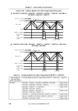
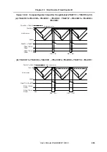
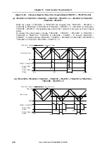
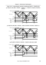
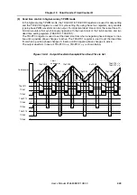
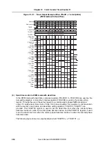
PWM mode with dead time settings
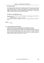
(a) Mode setting
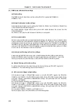
The PWM mode with dead time is set by setting TRnCTL1 register bits TRnMD4 to
TRnMD0 = 1001.
(b) Output level/output enable settings
Output level/output enable is set by setting the TRnOL0 to TRnOL7 and TRnOE0 to TRnOE7 bits
of the TRnIOC0 and TRnIOC3 registers.
Pin TORn0 performs toggle output upon cycle match (match between the counter and the
TRnCCR0 register).
Pin TORn7 is the output for A/D conversion. Set this pin as required.
(c) Error output enable
Set error output enable when normal phase/inverted phase simultaneous active is detected. Error
output is enabled by setting TRnIOC4 register bit TRnEOC to 1. Moreover, the pin for detecting
simultaneous active can also be set, by setting TRnIOC4 register bits TRnTBA2 to TRnTBA0. In
the PWM mode with dead time, INTTRnER does not become active, regardless of which value the
user sets to the TRnCCR0 to TRnCCR3 registers, except when the dead time setting is 0. When
an error occurs, this indicates an internal circuit fault.
(d) Interrupt and thinning out function settings
A peak interrupt (INTTRnCD) occurs upon a match between the TRnCCR0 register and the
counter (bit TRnIOE control is invalid). To output a peak interrupt, set TRnICE = 1. Use of the
thinning out function for peak interrupts is done with the TRnID4 to TRnID0 registers.
(e) Reload thinning out function setting
To set the reload timing to the same timing as the interrupt timing, set TRnOPT1 register bit
TRnRDE to 1. The reload timing occurs when TRnICE = 1.
(f) A/D conversion trigger output setting
A/D conversion trigger 0 (TRnADTRG0 signal) is set with TRnOPT2 register bits TRnAT04,
TRnAT02, and TRnAT01. The TRnCCR5 register match timing, TRnCCR4 register match timing,
and peak interrupt (INTTRnCD) enable/disable settings are performed with bits TRnAT04,
TRnAT02, and TRnAT01.
Do not set TRnAT05, TRnAT03, and TRnAT00 to “1”.
A/D conversion trigger 1 (TRnADTRG1 signal) is set with TRnOPT3 register bits TRnAT14,
TRnAT12, and TRnAT11. The TRnCCR5 register match timing, TRnCCR4 register match timing,
and peak interrupt (INTTRnCD) enable/disable settings are performed with bits TRnAT14,
TRnAT12, and TRnAT11.
Do not set bits TRnAT15, TRnAT13, and TRnAT10 to “1”.
Set the compare values of the TRnCCR4 and TRnCCR5 registers.
Summary of Contents for V850E/PH2
Page 6: ...6 Preface User s Manual U16580EE3V1UD00...
Page 16: ...16 User s Manual U16580EE3V1UD00...
Page 28: ...28 User s Manual U16580EE3V1UD00...
Page 32: ...32 User s Manual U16580EE3V1UD00...
Page 84: ...84 Chapter 2 Pin Functions User s Manual U16580EE3V1UD00 MEMO...
Page 144: ...144 Chapter 3 CPU Functions User s Manual U16580EE3V1UD00 MEMO...
Page 192: ...192 Chapter 5 Memory Access Control Function PD70F3187 only User s Manual U16580EE3V1UD00 MEMO...
Page 312: ...312 Chapter 9 16 Bit Timer Event Counter P User s Manual U16580EE3V1UD00 MEMO...
Page 534: ...534 Chapter 11 16 bit Timer Event Counter T User s Manual U16580EE3V1UD00...
Page 969: ...969 Chapter 20 Port Functions User s Manual U16580EE3V1UD00 MEMO...
Page 970: ...970 Chapter 20 Port Functions User s Manual U16580EE3V1UD00...
Page 976: ...976 Chapter 22 Internal RAM Parity Check Function User s Manual U16580EE3V1UD00 MEMO...
Page 984: ...984 Chapter 23 On Chip Debug Function OCD User s Manual U16580EE3V1UD00 MEMO...
Page 1006: ...1006 Chapter 24 Flash Memory User s Manual U16580EE3V1UD00 MEMO...
Page 1036: ...1036 Chapter 27 Recommended Soldering Conditions User s Manual U16580EE3V1UD00 MEMO...
Page 1046: ...1046 Appendix A Index User s Manual U16580EE3V1UD00 MEMO...
Page 1052: ...1052 User s Manual U16580EE3V1UD00...
Page 1053: ......

