629
Chapter 15
Asynchronous Serial Interface C (UARTC)
User’s Manual U16580EE3V1UD00
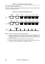
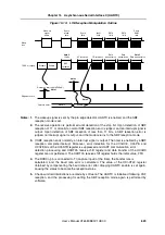
Figure 15-13:
LIN Reception Manipulation Outline
Notes: 1.
The wakeup signal is sent by the pin edge detector, UARTC is enabled, and the SBF
reception mode is set.
2.
The receive operation is performed until detection of the stop bit. Upon detection of SBF
reception of 11 or more bits, normal SBF reception end is judged, and an interrupt signal is
output. Upon detection of SBF reception of less than 11 bits, a SBF reception error is
judged, no interrupt signal is output, and the mode returns to the SBF reception mode.
3.
If SBF reception ends normally, an interrupt signal is output. The timer is enabled by a SBF
reception complete interrupt. Moreover, error detection for the UCnOVE, UCnPE, and
UCnFE bits of the UCnSTR register is suppressed and UART communication error
detection processing and UARTCn receive shift register and data transfer of the UCnRX
register are not performed. The UARTCn receive shift register holds the initial value, FFH.
4.
The RXDCn pin is connected to TI (capture input) of the timer, the transfer rate is
calculated, and the baud rate error is calculated. The value of the UCnCTL2 register
obtained by compensating the baud rate error after dropping UARTC enable is set again,
causing the status to become the reception status.
5.
Check-sum field distinctions are made by software. The UARTC is initialized following CSF
reception, and the processing for setting the SBF reception mode again is performed by
software.
Reception interrupt (INTUCnR)
Edge detection
Capture timer
Disable
Disable
Enable
TXDCn (output)
Enable
Note 2
13 bits
SBF
reception
Note 3
Note 4
Note 1
SF reception
ID reception
Data
transmission
Data
transmission
Note 5
Data transmission
Sleep
bus
Wake-up
signal
frame
Synch
break
field
Synch
field
Ident
field
DATA
field
DATA
field
Check
SUM
field
Summary of Contents for V850E/PH2
Page 6: ...6 Preface User s Manual U16580EE3V1UD00...
Page 16: ...16 User s Manual U16580EE3V1UD00...
Page 28: ...28 User s Manual U16580EE3V1UD00...
Page 32: ...32 User s Manual U16580EE3V1UD00...
Page 84: ...84 Chapter 2 Pin Functions User s Manual U16580EE3V1UD00 MEMO...
Page 144: ...144 Chapter 3 CPU Functions User s Manual U16580EE3V1UD00 MEMO...
Page 192: ...192 Chapter 5 Memory Access Control Function PD70F3187 only User s Manual U16580EE3V1UD00 MEMO...
Page 312: ...312 Chapter 9 16 Bit Timer Event Counter P User s Manual U16580EE3V1UD00 MEMO...
Page 534: ...534 Chapter 11 16 bit Timer Event Counter T User s Manual U16580EE3V1UD00...
Page 969: ...969 Chapter 20 Port Functions User s Manual U16580EE3V1UD00 MEMO...
Page 970: ...970 Chapter 20 Port Functions User s Manual U16580EE3V1UD00...
Page 976: ...976 Chapter 22 Internal RAM Parity Check Function User s Manual U16580EE3V1UD00 MEMO...
Page 984: ...984 Chapter 23 On Chip Debug Function OCD User s Manual U16580EE3V1UD00 MEMO...
Page 1006: ...1006 Chapter 24 Flash Memory User s Manual U16580EE3V1UD00 MEMO...
Page 1036: ...1036 Chapter 27 Recommended Soldering Conditions User s Manual U16580EE3V1UD00 MEMO...
Page 1046: ...1046 Appendix A Index User s Manual U16580EE3V1UD00 MEMO...
Page 1052: ...1052 User s Manual U16580EE3V1UD00...
Page 1053: ......

