MC96F6432
June 22, 2018 Ver. 2.9
325
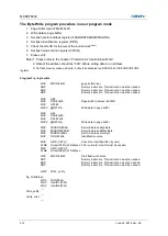
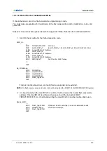
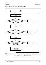
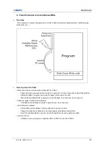
Descript of Flowchart
•
①
Initialization
-
Set the LVR/LVI
Check the power by LVR/LVI and do not execute under unstable or low power.
-
Initialize User_ID1/2/3
-
Set Flash Sector Address High/Middle/Low to Dummy address
Dummy address is set to unused area range in flash.
•
②
Decide to Write
-
When the Erase/Write are determined, set flag. Do not directly Erase/Write in flash.
-
Make the user data.
•
③
Check and Set User_ID1/2/3
-
In the middle of source, insert code which can check and set the flags.
-
By setting the User_ID 1/2/3 sequentially and identify the flow of the program.
•
④
Set Flash Sector Address
-
Set address to real area range shortly before Erase/Write in flash.
Set to Dummy address after Erase/Write
Even if invalid work occurred, it will be Erase/Write in Dummy address in flash.
•
⑤
Check Flags
-
If every flag(User_ID1/2/3, LVI, Flash Address Min/Max) was set, than do Erase/Write.
-
If the Flash Sector Address is outside of Min/Max, do not execute
-
Address Min/Max is set to unused area.
•
⑥
Initialize Flags
-
Initialize User_ID1/2/3
-
Set Flash Sector Address to Dummy Address
•
Sample Source
-
Refer to the ABOV homepage.
-
It is created based on the MC97F2664.
-
Each product should be modified according to the Page Buffer Size and Flash Size
Etc
•
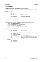
Protection by Configure option
-
S
et flash protection by MCU Write Tool(OCD, PGM+, etc…)
Vector Area :
00H~FFH
Specific Area :
3.7k Bytes (Address 0100H
– 0FFFH)
1.7k Bytes (Address 0100H
– 07FFH)
768 Bytes (Address 0100H
– 03FFH)
256 Bytes (Address 0100H
– 01FFH)
-
The range of protection may be different each product.
Summary of Contents for MC96F6432 Series
Page 24: ...MC96F6432 24 June 22 2018 Ver 2 9 4 Package Diagram Figure 4 1 48 Pin LQFP 0707 Package...
Page 25: ...MC96F6432 June 22 2018 Ver 2 9 25 Figure 4 2 44 Pin MQFP Package...
Page 26: ...MC96F6432 26 June 22 2018 Ver 2 9 Figure 4 3 32 Pin LQFP Package...
Page 27: ...MC96F6432 June 22 2018 Ver 2 9 27 Figure 4 4 32 Pin SOP Package...
Page 28: ...MC96F6432 28 June 22 2018 Ver 2 9 Figure 4 5 28 Pin SOP Package...


