MC96F6432
June 22, 2018 Ver. 2.9
177
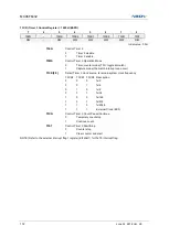
T4PCR1 (Timer 4 PWM Control Register 1) : 1003H (ESFR)
7
6
5
4
3
2
1
0
PWM4E
ESYNC
BMOD
PHLT
UPDT
UALL
NOPS1
NOPS0
R/W
R/W
R/W
R/W
R/W
R/W
R/W
R/W
Initial value : 00H
PWM4E
Control Timer 4 Mode
0
Select timer/counter or capture mode of Timer 4
1
Select 10-bit PWM mode of Timer 4
ESYNC
Select the Operation of External Sync with the BLNK pin
0
Disable external sync operation
1
Enable external sync operation
(The all PWM4xA/PWM4xB pins are high-impedance outputs
on rising edge of the BLNK input pin. Where x= A, B and C)
BMOD
Control Back-to-Back Mode Operation
0
Disable back-to-back mode (up count only)
1
Enable back-to-back mode (up/down count only)
PHLT
Control Timer 4 PWM Operation
0
Run 10-bit PWM
1
Stop 10-bit PWM (counter hold and output disable)
UPDT
Select the Update Timer of T4PPR/T4ADR/T4BDR/T4CDR
0
Update at period match of T4CNT and T4PPR
1
Update at any time when written
UALL
Control Update All Duty Registers (T4ADR/T4BDR/T4CDR)
0
Write a duty register separately
1
Write all duty registers via Timer 4 PWM A duty register
(T4ADR)
NOPS[1:0]
Select on-Overlap Prescaler
NOPS1 NOPS0
Description
0
0
f
PWM
/1
0
1
f
PWM
/2
1
0
f
PWM
/4
1
1
f
PWM
/8
NOTE) Where the f
PWM
is the clock frequency of the Timer 4 PWM.
Summary of Contents for MC96F6432 Series
Page 24: ...MC96F6432 24 June 22 2018 Ver 2 9 4 Package Diagram Figure 4 1 48 Pin LQFP 0707 Package...
Page 25: ...MC96F6432 June 22 2018 Ver 2 9 25 Figure 4 2 44 Pin MQFP Package...
Page 26: ...MC96F6432 26 June 22 2018 Ver 2 9 Figure 4 3 32 Pin LQFP Package...
Page 27: ...MC96F6432 June 22 2018 Ver 2 9 27 Figure 4 4 32 Pin SOP Package...
Page 28: ...MC96F6432 28 June 22 2018 Ver 2 9 Figure 4 5 28 Pin SOP Package...


