MC96F6432
264
June 22, 2018 Ver. 2.9
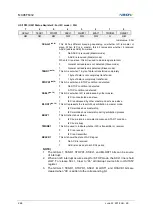
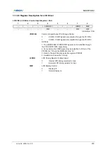
USI1CR2 (USI1 Control Register 2: For UART, SPI, and I2C mode) : EAH
7
6
5
4
3
2
1
0
DRIE1
TXCIE1
RXCIE1
WAKEIE1
TXE1
RXE1
USI1EN
DBLS1
R/W
R/W
R/W
R/W
R/W
R/W
R/W
R/W
Initial value : 00H
DRIE1
Interrupt enable bit for data register empty (only UART and SPI mode).
0
Interrupt from DRE1 is inhibited (use polling)
1
When DRE1 is set, request an interrupt
TXCIE1
Interrupt enable bit for transmit complete (only UART and SPI mode).
0
Interrupt from TXC1 is inhibited (use polling)
1
When TXC1 is set, request an interrupt
RXCIE1
Interrupt enable bit for receive complete (only UART and SPI mode).
0
Interrupt from RXC1 is inhibited (use polling)
1
When RXC1 is set, request an interrupt
WAKEIE1
Interrupt enable bit for asynchronous wake in STOP mode. When device
is in stop mode, if RXD1 goes to low level an interrupt can be requested
to wake-up system. (only UART mode). At that time the DRIE1 bit and
USI1ST1 register value should be set to
‘0b’ and “00H”, respectively.
0
Interrupt from Wake is inhibited
1
When WAKE1 is set, request an interrupt
TXE1
Enables the transmitter unit (only UART and SPI mode).
0
Transmitter is disabled
1
Transmitter is enabled
RXE1
Enables the receiver unit (only UART and SPI mode).
0
Receiver is disabled
1
Receiver is enabled
USI1EN
Activate USI1 function block by supplying.
0
USI1 is disabled
1
USI1 is enabled
DBLS1
This bit selects receiver sampling rate (only UART)
0
Normal asynchronous operation
1
Double Speed asynchronous operation
Summary of Contents for MC96F6432 Series
Page 24: ...MC96F6432 24 June 22 2018 Ver 2 9 4 Package Diagram Figure 4 1 48 Pin LQFP 0707 Package...
Page 25: ...MC96F6432 June 22 2018 Ver 2 9 25 Figure 4 2 44 Pin MQFP Package...
Page 26: ...MC96F6432 26 June 22 2018 Ver 2 9 Figure 4 3 32 Pin LQFP Package...
Page 27: ...MC96F6432 June 22 2018 Ver 2 9 27 Figure 4 4 32 Pin SOP Package...
Page 28: ...MC96F6432 28 June 22 2018 Ver 2 9 Figure 4 5 28 Pin SOP Package...


