MC96F6432
216
June 22, 2018 Ver. 2.9
11.12.20.2 USI0 I2C Master Receiver
To operate I2C in master receiver, follow the recommended steps below.
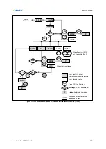
1. Enable I2C by setting USI0MS[1:0]
bits in USI0CR1 and USI0EN bit in USI0CR2. This provides main
clock to the peripheral.
2. Load SLA0+R into the USI0DR where SLA is address of slave device and R is transfer direction from
the viewpoint of the master. For master receiver, R is
‘1’. Note that USI0DR is used for both address
and data.
3. Configure baud rate by writing desired value to both USI0SCLR and USI0SCHR for the Low and High
period of SCL0 line.
4. Configure the USI0SDHR to decide when SDA0 changes value from falling edge of SCL0. If SDA0
should change in the middle of SCL0 LOW period, load half the value of USI0SCLR to the USI0SDHR.
5. Set the STARTC0 bit in USI0CR4. This transmits a START condition. And also configure how to handle
interrupt and ACK signal. When the STARTC0 bit is set, 8-bit data in USI0DR is transmitted out
according to the baud-rate.
6. This is ACK signal processing stage for address packet transmitted by master. When 7-bit address and
1-bit transfer direction is transmitted to target slave device, the master can know whether the slave
acknowledged or not in the 9
th
high period of SCL0. If the master gains bus mastership, I2C generates
GCALL interrupt regardless of the reception of ACK from the slave device. When I2C loses bus
mastership during arbitration process, the MLOST0 bit in USI0ST2 is set, and I2C waits in idle state or
can be operate as an addressed slave. To operate as a slave when the MLOST0 bit in USI0ST2 is set,
the ACK0EN bit in USI0CR4 must be set and the received 7-bit address must equal to the USI0SLA[6:0]
bits in USI0SAR. In this case I2C operates as a slave transmitter or a slave receiver (go to appropriate
section). In this stage, I2C holds the SCL0 LOW. This is because to decide whether I2C continues serial
transfer or stops communication. The following steps continue assuming that I2C does not lose
mastership during first data transfer.
I2C (Master) can choose one of the following cases according to the reception of ACK signal from slave.
1) Master receives ACK signal from slave, so continues data transfer because slave can prepare and
transmit more data to master. Configure ACK0EN bit in USI0CR4 to decide whether I2C ACKnowledges
the next data to be received or not.
2) Master stops data transfer because it receives no ACK signal from slave. In this case, set the
STOPC0 bit in USI0CR4.
3) Master transmits repeated START condition due to no ACK signal from slave. In this case, load
SLA0+R/W into the USI0DR and set STARTC0 bit in USI0CR4.
After doing one of the actions above, clear to
“0b” all interrupt source bits in USI0ST2 to release SCL0
line. In case of 1), move to step 7. In case of 2), move to step 9 to handle STOP interrupt. In case of 3),
move to step 6 after transmitting the data in USI0DR and if transfer direction bit is
‘0’ go to master
transmitter section.
7. 1-Byte of data is being received.
8. This is ACK signal processing stage for data packet transmitted by slave. I2C holds the SCL0 LOW.
When 1-Byte of data is received completely, I2C generates TEND0 interrupt.
I2C0 can choose one of the following cases according to the RXACK0 flag in USI0ST2.
1) Master continues receiving data from slave. To do this, set ACK0EN bit in USI0CR4 to ACKnowledge
the next data to be received.
2) Master wants to terminate data transfer when it receives next data by not generating ACK signal. This
can be done by clearing ACK0EN bit in USI0CR4.
3) Because no ACK signal is detected, master terminates data transfer. In this case, set the STOPC0 bit
in USI0CR4.
4) No ACK signal is detected, and master transmits repeated START condition. In this case, load
SLA0+R/W into the USI0DR and set the STARTC0 bit in USI0CR4.
After doing one of the actions above clear to
“0b” all interrupt source bits in USI0ST2 to release SCL0
line. In case of 1) and 2), move to step 7. In case of 3), move to step 9 to handle STOP interrupt. In case
of 4), move to step 6 after transmitting the data in USI0DR, and if transfer direction bit is
‘0’ go to master
transmitter section.
Summary of Contents for MC96F6432 Series
Page 24: ...MC96F6432 24 June 22 2018 Ver 2 9 4 Package Diagram Figure 4 1 48 Pin LQFP 0707 Package...
Page 25: ...MC96F6432 June 22 2018 Ver 2 9 25 Figure 4 2 44 Pin MQFP Package...
Page 26: ...MC96F6432 26 June 22 2018 Ver 2 9 Figure 4 3 32 Pin LQFP Package...
Page 27: ...MC96F6432 June 22 2018 Ver 2 9 27 Figure 4 4 32 Pin SOP Package...
Page 28: ...MC96F6432 28 June 22 2018 Ver 2 9 Figure 4 5 28 Pin SOP Package...

