MC96F6432
42
June 22, 2018 Ver. 2.9
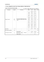
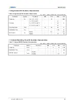
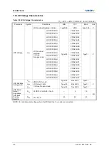
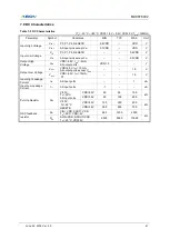
Table 7-9 DC Characteristics (Continued)
(T
A
= -40°C ~ +85°C, VDD= 1.8V ~ 5.5V, VSS= 0V, f
XIN
= 12MHz)
Parameter
Symbol
Condition
MIN
TYP
MAX
Unit
Supply Current
I
DD1
(RUN)
f
XIN
= 12MHz, VDD= 5V±10%
–
3.0
6.0
mA
f
XIN
= 10MHz, VDD= 3V±10%
–
2.2
4.4
f
IRC
= 16MHz, VDD= 5V±10%
–
3.0
6.0
I
DD2
(IDLE)
f
XIN
= 12MHz, VDD= 5V±10%
–
2.0
4.0
mA
f
XIN
= 10MHz, VDD= 3V±10%
–
1.3
2.6
f
IRC
= 16MHz, VDD= 5V±10%
–
1.5
3.0
I
DD3
f
XIN
= 32.768kHz
VDD= 3V±10%
T
A
= 25°C
Sub RUN
–
50.0
80.0
uA
I
DD4
Sub IDLE
–
8.0
16.0
uA
I
DD5
STOP, VDD= 5V±10%, T
A
= 25°C
–
0.5
3.0
uA
NOTES) 1. Where the f
XIN
is an external main oscillator, f
SUB
is an external sub oscillator, the f
IRC
is an internal
RC oscillator, and the fx is the selected system clock.
2. All supply current items don
’t include the current of an internal Watch-dog timer RC (WDTRC)
oscillator and a peripheral block.
3. All supply current items include the current of the power-on reset (POR) block.
Summary of Contents for MC96F6432 Series
Page 24: ...MC96F6432 24 June 22 2018 Ver 2 9 4 Package Diagram Figure 4 1 48 Pin LQFP 0707 Package...
Page 25: ...MC96F6432 June 22 2018 Ver 2 9 25 Figure 4 2 44 Pin MQFP Package...
Page 26: ...MC96F6432 26 June 22 2018 Ver 2 9 Figure 4 3 32 Pin LQFP Package...
Page 27: ...MC96F6432 June 22 2018 Ver 2 9 27 Figure 4 4 32 Pin SOP Package...
Page 28: ...MC96F6432 28 June 22 2018 Ver 2 9 Figure 4 5 28 Pin SOP Package...


