MC96F6432
June 22, 2018 Ver. 2.9
225
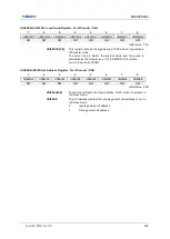
USI0SCLR (USI0 SCL Low Period Register: For I2C mode) : E6H
7
6
5
4
3
2
1
0
USI0SCLR7
USI0SCLR6
USI0SCLR5
USI0SCLR 4
USI0SCLR 3
USI0SCLR 2
USI0SCLR 1
USI0SCLR 0
R/W
R/W
R/W
R/W
R/W
R/W
R/W
R/W
Initial value : 3FH
USI0SCLR[7:0]
This register defines the high period of SCL0 when it operates in
I2C master mode.
The base clock is SCLK, the system clock, and the period is
calculated by the formula: t
SCLK
X (4 X US2) where
t
SCLK
is the period of SCLK.
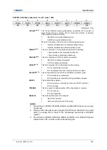
USI0SAR (USI0 Slave Address Register: For I2C mode) : DDH
7
6
5
4
3
2
1
0
USI0SLA6
USI0SLA5
USI0SLA4
USI0SLA3
USI0SLA2
USI0SLA1
USI0SLA0
USI0GCE
R/W
R/W
R/W
R/W
R/W
R/W
R/W
R/W
Initial value : 00H
USI0SLA[6:0]
These bits configure the slave address of I2C when it operates in
I2C slave mode.
USI0GCE
This bit decides whether I2C allows general call address or not in
I2C slave mode.
0
Ignore general call address
1
Allow general call address
Summary of Contents for MC96F6432 Series
Page 24: ...MC96F6432 24 June 22 2018 Ver 2 9 4 Package Diagram Figure 4 1 48 Pin LQFP 0707 Package...
Page 25: ...MC96F6432 June 22 2018 Ver 2 9 25 Figure 4 2 44 Pin MQFP Package...
Page 26: ...MC96F6432 26 June 22 2018 Ver 2 9 Figure 4 3 32 Pin LQFP Package...
Page 27: ...MC96F6432 June 22 2018 Ver 2 9 27 Figure 4 4 32 Pin SOP Package...
Page 28: ...MC96F6432 28 June 22 2018 Ver 2 9 Figure 4 5 28 Pin SOP Package...


