MC96F6432
158
June 22, 2018 Ver. 2.9
11.8.6 10-Bit Timer 4 PWM Mode
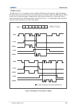
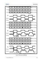
The timer 4 has a high speed PWM (Pulse Width Modulation) function. In PWM mode, the 6-channel pins output
up to 10-bit resolution PWM output. This pin should be configured as a PWM output by set PWM4
E to ‘1’. When
the value of 2bit +T4CNT and T4PPRH/L are identical in timer 4, a period match signal is generated and the
interrupt of timer 4 occurs. In 10-bit PWM mode, A, B, C, bottom(underflow) match signal are generated when the
10-bit counter value are identical to the value of T4xDRH/L. The period of the PWM output is determined by the
T4PPRH/L (PWM period register), T4xDRH/L (each channel PWM duty register).
PWM Period = [T4PPRH/T4PPRL ] X Source Clock
PWM Duty(A-ch) = [ T4ADRH/T4ADRL ] X Source Clock
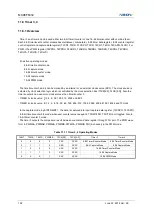
Table 11-12 PWM Frequency vs. Resolution at 8 MHz
Resolution
Frequency
T4CK[3:0]=0001 (250ns)
T4CK[3:0]=0010 (500ns) T4CK[3:0]=0100 (2us)
10 Bit
3.9kHz
1.95kHz
0.49kHz
9 Bit
7.8kHz
3.9kHz
0.98kHz
8 Bit
15.6kHz
7.8kHz
1.95kHz
7 Bit
31.2kHz
15.6kHz
3.91kHz
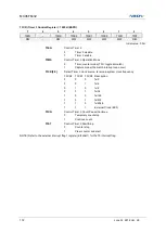
The POLxA bit of T4PCR3 register decides the polarity of duty cycle. If the duty value is set same to the period
value, the PWM output is determined by the bit POLxA (1: High, 0: Low). And if the duty value is set to "00H", the
PWM output is determined by the bit POLxA (1: Low, 0: High).
Table 11-13 PWM Channel Polarity
PHLT:PxxOE
POLxA
POLBO
POLxB
PWM4xA Pin Output
PWM4xB Pin Output
0x, x0, 00
0
0
0
Low-level
Low-level
1
Low-level
High-level
1
x
Low-level
Low-level
1
0
0
High-level
High-level
1
High-level
Low-level
1
x
High-level
High-level
11
0
x
0
Positive-phase
Positive-Phase
1
Positive-phase
Negative-Phase
1
x
0
Negative-Phase
Negative-Phase
1
Negative-Phase
Positive-phase
Summary of Contents for MC96F6432 Series
Page 24: ...MC96F6432 24 June 22 2018 Ver 2 9 4 Package Diagram Figure 4 1 48 Pin LQFP 0707 Package...
Page 25: ...MC96F6432 June 22 2018 Ver 2 9 25 Figure 4 2 44 Pin MQFP Package...
Page 26: ...MC96F6432 26 June 22 2018 Ver 2 9 Figure 4 3 32 Pin LQFP Package...
Page 27: ...MC96F6432 June 22 2018 Ver 2 9 27 Figure 4 4 32 Pin SOP Package...
Page 28: ...MC96F6432 28 June 22 2018 Ver 2 9 Figure 4 5 28 Pin SOP Package...

