MC96F6432
188
June 22, 2018 Ver. 2.9
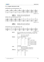
SPICR (SPI 2 Control Register) : B5H
7
6
5
4
3
2
1
0
SPIEN
FLSB
MS
CPOL
CPHA
DSCR
SCR1
SCR0
R/W
R/W
R/W
R/W
R/W
R/W
R/W
R/W
Initial value : 00H
SPIEN
This bit controls the SPI 2 operation
0
Disable SPI 2 operation
1
Enable SPI 2 operation
FLSB
This bit selects the data transmission sequence
0
MSB first
1
LSB first
MS
This bit selects whether Master or Slave mode
0
Slave mode
1
Master mode
CPOL
CPHA
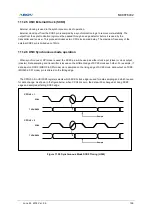
This two bits control the serial clock (SCK2) mode.
Clock polarity(CPOL) bit determine SCK2
’s value at idle mode.
Clcok phase (CPHA) bit determine if data are sampled on the leading or
trailing edge of SCK2.
CPOL CPHA Leading edge
Trailing edge
0
0
Sample (Rising)
Setup (Falling)
0
1
Setup (Rising)
Sample (Falling)
1
0
Sample (Falling)
Setup (Rising)
1
1
Setup (Falling)
Sample (Rising)
DSCR
SCR[2:0]
These three bits select the SCK2 rate of the device configured as a
master. When DSCR bit is written one, SCK2 will be doubled in master
mode.
DSCR SCR1
SCR0
SCK2 frequency
0
0
0
fx/4
0
0
1
fx/16
0
1
0
fx/64
0
1
1
fx/128
1
0
0
fx/2
1
0
1
fx/8
1
1
0
fx/32
1
1
1
fx/64
Summary of Contents for MC96F6432 Series
Page 24: ...MC96F6432 24 June 22 2018 Ver 2 9 4 Package Diagram Figure 4 1 48 Pin LQFP 0707 Package...
Page 25: ...MC96F6432 June 22 2018 Ver 2 9 25 Figure 4 2 44 Pin MQFP Package...
Page 26: ...MC96F6432 26 June 22 2018 Ver 2 9 Figure 4 3 32 Pin LQFP Package...
Page 27: ...MC96F6432 June 22 2018 Ver 2 9 27 Figure 4 4 32 Pin SOP Package...
Page 28: ...MC96F6432 28 June 22 2018 Ver 2 9 Figure 4 5 28 Pin SOP Package...


