Copyright © Siemens AG 2016. All rights reserved
477
ERTEC 200P-2 Manual
Technical data subject to change
Version
1.0
The values for Rv, Cin, Cout has to be calculated accordingly
.
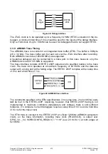
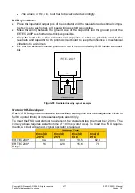
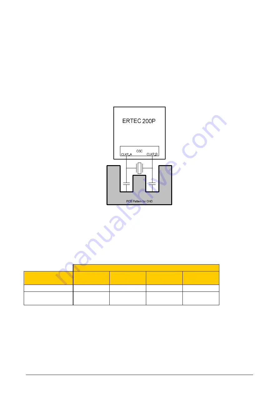
PCB layout hints:
Place the input and output pins of the oscillator and the resonator and external compo-
nents close to each other, and keep wiring as short as possible.
Make the wiring between the ground side of the capacitor and the ground pin of the
ERTEC 200P as short and as thick as possible.
Keep the lead wire of the resonator and capacitor as short as possible, and fix the
resonator and capacitor to the printed circuit board to keep the influence of mechanical
vibrations to a minimum.
Lay out the external constant portion so that it is surrounded by GND insofar as possi-
ble.
Figure 51:
Oscillator Circuitry Layout Example
Note for HW-Developer:
Each PCB Design has to measure the oscillator startup time and must adjust the circuit to
fulfill required timing or increase reset puls accordingly.
To meet the FSU (fast startup) requirement, the crystal startup time must be < 20 ms. The
circuity above requires a startup time of ~80 ms (worst case). To meet the FSU require-
ments, a circuit with an ext. crystal oscillator is required.
Startup Time
t[ms] @
-20°C
t[ms] @
25°C
t[ms] @
60°C
t[ms] @
85°C
ERTEC 200P
n.a.
9,04
13,5
82,4
ERTEC 200P
Step2
5,6
9,28
15,6
78
Содержание ERTEC 200P
Страница 1: ...ERTEC 200P 2 Enhanced Real Time Ethernet Controller Manual ...
Страница 309: ...Copyright Siemens AG 2016 All rights reserved 309 ERTEC 200P 2 Manual Technical data subject to change Version 1 0 ...
Страница 492: ...Copyright Siemens AG 2016 All rights reserved 492 ERTEC 200P 2 Manual Technical data subject to change Version 1 0 ...


