Copyright © Siemens AG 2016. All rights reserved
163
ERTEC 200P-2 Manual
Technical data subject to change
Version 1.0
2.3.5.4.4
Control of an External Driver
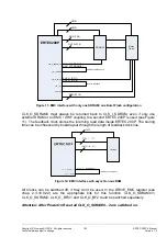
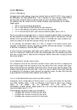
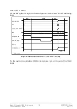
The signals DTXR and XOE_DRIVER at the EMC are used to control external drivers
(timing, see 2.3.5.5.1 and 2.3.5.5.2). These signals can only be used for asynchronous
memory. The use of these signals is optional.
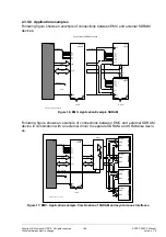
As the signals for controlling the drivers are always activated irrespective of the address
range of the asynchronous EMC interface (CS0 – CS3) and not on a chip select-specific
basis, the driver becomes active even when memory without/before the driver is ac-
cessed; in this case two devices would drive the data bus for the EMC.
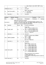
To prevent this from happening, a chip select-specific enable for driver control can be
configured with the SCRB register
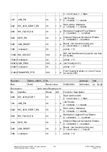
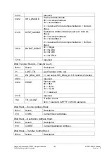
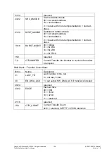
EXT_DRIVER_EN
Driver control is disabled after a reset. To allow the flash block in the NOR flash boot (see
0) to be operated both before and after the driver, the driver control information
(
EXT_DRIVER_DISABLE_CS0)
for address range: 0x3000_0000 – 0x33FF_FFFF (chip
select 0) is also latched to
EXT_DRIVER_EN.CS0_ENABLE
over EMC pin XRDY_BF
when the reset is cleared. The integrated pull-up means that control for an external driver
is deactivated by default and needs to be activated with a pull-down for the module.
2.3.5.4.5
QVZ Acknowledgement Delay
If the ready signal does not respond in time with asynchronous RAMs (…ROMs, all de-
vices with ready), an interrupt is generated and the address that has generated the error
is saved. This is known as QVZ (
Quittungsverzug
, acknowledgement delay) monitoring.
The signals ASYNC_WAIT and BF_RDY are monitored. The QVZ interrupt
(EMC_QVZ_INT, see 2.3.2.14) is triggered synchronously to the AHB clock.
All read and write access to external asynchronous RAMs interrupts the SDRAM refresh
cycles until access is ended. The value MAX_EXT_WAIT is the limit for one complete
instance of burst access on the RAM interface, not at the AHB bus. For example, 32-bit
read access to an 8-bit block is converted to a burst with 4 reads. All 4 reads must be
carried out within the set time window (MAX_EXT_WAIT).
The memory is addressed at the address of EMC Peripheral Bank 0. With NAND flash
with a
page size of 512 bytes
, GPIO31 is used as chip select (CE), i.e. there must be no
XCS_PER0 signal connected for selection at the blocks. This is important as NAND
flashes with a page size of 512 bytes do not permit any change in the CS signal during
address byte transfer and would otherwise not respond correctly.
Содержание ERTEC 200P
Страница 1: ...ERTEC 200P 2 Enhanced Real Time Ethernet Controller Manual ...
Страница 309: ...Copyright Siemens AG 2016 All rights reserved 309 ERTEC 200P 2 Manual Technical data subject to change Version 1 0 ...
Страница 492: ...Copyright Siemens AG 2016 All rights reserved 492 ERTEC 200P 2 Manual Technical data subject to change Version 1 0 ...


