background image


Copyright © Siemens AG 2016. All rights reserved 

396 

ERTEC 200P-2 Manual 

Technical data subject to change 


Version  1.0 


controlled by the PHY 

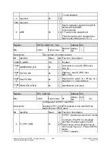
1: LED: P2_XLINK_XACTIVITY is 
controlled by the SW 

7dt4  reserved 

xh 

    No function, should always be '0000' 

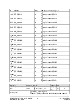
8  P1_XLINK_STATUS_SW 

xh 

r  w 

0: LED: P1_XLINK_STATUS is '0', set 
by the SW 

1: LED: P1_XLINK_STATUS is '1', set 
by the SW 

9  P1_XACTIVITY_SW 

xh 

r  w 

0: LED: P1_XLINK_XACTIVITY is '0', 
set by the SW 

1: LED: P1_XLINK_XACTIVITY is '1', 
set by the SW 

10  P2_XLINK_STATUS_SW 

xh 

r  w 

0: LED: P2_XLINK_STATUS is '0', set 
by the SW 

1: LED: P2_XLINK_STATUS is '1', set 
by the SW 

11  P2_XACTIVITY_SW 

xh 

r  w 

0: LED: P2_XLINK_XACTIVITY is '0', 
set by the SW 

1: LED: P2_XLINK_XACTIVITY is '1', 
set by the SW 

15dt1

reserved 

xh 


No function, should always be '0000' 

16 P1_XLINK_STATUS_PHY  xh 

r

h  

P1_XLINK_STATUS controlled by the 
PHY 

17  P1_XACTIVITY_PHY 

xh 

r

h  

P1_XACTIVITY controlled by the PHY 

18 P2_XLINK_STATUS_PHY  xh 

r

h  

P2_XLINK_STATUS controlled by the 
PHY 

19  P2_XACTIVITY_PHY 

xh 

r

h  

P2_XACTIVITY controlled by the PHY 


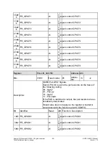
Register: 

ACCESS_ERROR_SCRB 

Address: 74h 

Bits: 

31dt0 

Reset value: 

2000000
0h 

Attribu-
tes: 

(r)(h

(w) 

Description: 

SCRB Access Error 

Bit  Identifier 

Reset Attr. Function / Description 

7dt0  APB_ADDRESS 

xh 

r

w Erroneous APB address in SCRB 

27dt8 Reserved 

xh 

    READ_DATA = (others -= '0') 

29dt2 APB_SIZE 

2h 

r    Clamped at 10 (word access) as only 

Содержание ERTEC 200P

Страница 1: ...ERTEC 200P 2 Enhanced Real Time Ethernet Controller Manual ...

Страница 2: ...HE CONTENTS OF THESE WEB SITES AND ELECTRONIC DOCUMENTS NOR DOES SIEMENS ADOPT THESE WEB SITES AND ELECTRONIC DOCUMENTS AND THEIR CONTENTS AS THEIR OWN YOU THEREFORE USE THESE LINKS AT YOUR OWN RISK SINCE SIEMENS IS NOT RESPONSIBLE FOR LINKED CONTENTS AND INFORMATION ON THE WEB SITES AND ELECTRONIC DOCUMENTS OF THIRD PARTIES THIS INFORMATION IS NOT CHECKED BY SIEMENS COPYRIGHT SIEMENS AG 2016 ALL ...

Страница 3: ...ERTEC function groups in details and provides information that you must take into account when configuring your own PROFINET IO device hardware The manual serves as a reference for software developers The address areas and register contents are described in detail for all function groups Structure of this Manual o Section 1 Introduction o Section 2 Description of functions o Section 3 IO Interface...

Страница 4: ...at the end of the manual Additional Support If you have questions regarding use of the described block that are not addressed in the documentation please contact your Siemens representative Please send your written questions comments and suggestions regarding the manual to the hotline via the e mail address indicated above In addition you can receive general information current product information...

Страница 5: ...nts should only be connected to the enterprise network or the internet if and to the extent necessary and with appropriate secu rity measures e g use of firewalls and network segmentation in place Additionally Siemens guidance on appropriate security measures should be taken intoac count For more information about industrial security please visit http www siemens com industrialsecurity Siemens pro...

Страница 6: ...sor Subsystem ARM926 25 2 3 1 1 Features 26 2 3 1 2 Block diagram 26 2 3 1 3 ARM926EJ S processor 27 2 3 1 3 1 Cache structure of ARM926EJ S 27 2 3 1 3 2 ARM926 Tightly Coupled Memories ARM926_TCM 28 2 3 1 3 3 Memory Management Unit MMU 29 2 3 1 3 4 Bus Interface of the ARM926 Processor 30 2 3 1 3 5 ARM926 Embedded Trace Macrocell ETM9 Trace Buffer ETB11 30 2 3 1 4 Debug Support 31 2 3 1 4 1 Debug...

Страница 7: ... 103 2 3 4 1 1 AHB interfaces 104 2 3 4 1 2 Job priorities 104 2 3 4 1 3 Details 104 2 3 4 1 4 Usage 114 2 3 4 1 5 Result 115 2 3 4 1 6 Memory 116 2 3 4 1 7 Interrupts 117 2 3 4 2 ERTEC 200P GDMA Use Cases 117 2 3 4 2 1 Using the Job Start and HW_REQ Signal List 117 2 3 4 2 2 DMA with UART Interface 125 2 3 4 3 GDMA IP Bugs 125 2 3 4 4 Address Mapping 126 2 3 4 5 Register Description 129 2 3 5 EMC...

Страница 8: ...synchronous JTAG Reset 244 2 3 9 4 4 Asynchronous ARM926 Watchdog Reset 245 2 3 9 4 5 Asynchronous Software Reset for ERTEC 200P Without PN IP 245 2 3 9 4 6 Asynchronous Software Reset for PN IP 245 2 3 9 4 7 Asynchronous Software Reset for the ARM926EJ S Core 246 2 3 9 4 8 Synchronous Software Reset PN IP PER IF Host Interface 246 2 3 10 APB Peripherals 247 2 3 10 1 I Filter 248 2 3 10 1 1 Operat...

Страница 9: ...3 2 3 10 8 5 Address Mapping 356 2 3 10 8 6 Register Description 357 2 3 10 9 SCRB System Control Register Block 365 2 3 10 9 1 Hardware Identifier Register 365 2 3 10 9 2 Boot Register 366 2 3 10 9 3 Config Register 366 2 3 10 9 4 Reset Registers 367 2 3 10 9 5 ACCESS_ERROR and QVZ Register 368 2 3 10 9 6 PLL Status Register 368 2 3 10 9 7 Memory Swapping 368 2 3 10 9 8 ARM Control Register 369 2...

Страница 10: ...egrated PHY 464 3 3 3 2 MDIO Timing 464 3 3 3 2 1 MDIO Timing at the Integrated PHY 465 3 3 3 3 Integrated PHY Timing 465 3 3 3 3 1 PHY FX Timing 465 3 3 3 3 2 PHY LED Timing 465 3 3 3 4 PNPLL Timing 465 3 3 3 4 1 Timing for time synchronization 467 3 3 4 SPI Timing 468 3 3 4 1 SPI1 468 3 3 4 2 SPI2 468 3 3 5 UART Timing 470 3 3 5 1 UART1 470 3 3 5 2 UART2 470 3 3 5 3 UART3 470 3 3 5 4 UART4 470 3...

Страница 11: ...or 489 4 8 4 1 following crystal break 489 4 8 4 2 upon temporary clock failure 489 4 8 5 Readiness of internal resources once a reset is cleared 490 4 9 Pull up Pull down Resistor Values 490 4 10 Schmitt Trigger Characteristics 490 4 11 Module and ASIC Code Chip ID 490 4 12 Power dissipation 491 5 PACKAGE 493 5 1 Package Drawing 493 5 2 Ball Layout 493 5 3 Marking Printed 495 5 3 1 Order codes 49...

Страница 12: ...Block diagram of the host interface 182 Figure 20 XHIF Symbol and Signals 184 Figure 21 XHIF interface adjustment 186 Figure 22 Block diagram of the peripheral interface 198 Figure 23 Block diagram of PN ICU for PN_IRQx 0 1 0 group interrupts 231 Figure 24 Block diagram of PN MUX for PN_IRQx 2 1 15 2 single interrupts 232 Figure 25 PNPLL with 3 application time blocks application connection 233 Fi...

Страница 13: ... ARM926 trace interface 472 Figure 50 Spike Filter Implementation 475 Figure 51 Oscillator Circuitry Layout Example 477 Figure 52 Connection of an external oscillator 478 Figure 53 Recommended for PLL Power Supply Filter 479 Figure 54 UTP circuit 482 Figure 55 FX circuit 484 Figure 56 FX circuit unused pins 485 Figure 57 SD level translation circuit 486 Figure 58 Recommendation for handling specia...

Страница 14: ...10 Host INTB Interrupt sources 69 Table 11 DMA Table of HW_JOB_START_Signals 118 Table 12 DMA Table of HW_DMA_REQ Signals 121 Table 13 The DMA RAM address space 154 Table 14 EMC Connection to the Memory devices 168 Table 15 EMC Address map 169 Table 16 Overview of ERTEC 200P clocks 236 Table 17 Data width of peripherals 247 Table 18 Sample filter times for I filter 250 Table 19 Timing parameters f...

Страница 15: ...ack together multiple devices This significantly reduces the cut through time which in turn leads to much shorter cycle times 1 1 1 Mechanisms for PROFINET IO NRT communication The basis for NRT requirements is switch functions for standard Ethernet NRT with NRT fragmentation for shorter send clocks This is what is known as the address based forwarding of frames The required function is specified ...

Страница 16: ...ng time in each individual node is a defining factor for performance for systems with a large number of nodes and in particular for large line depths IRT uses super fast forwarding locally administrated MultiCast frames with frame ID in Octet 1 2 This allows each IRT High Performance device to forward after just the first two bytes of the DA address The cut through time is again significantly redu...

Страница 17: ...Byte D TCM 256 0 KByte Debug compatibility with embedded ICE with JTAG interface ETM with ETB Embedded Trace Buffer Memory Management Unit MMU Bus structure Internal 32 bit structure Multi layer architecture with parallel multimaster to multislaves access structure 125 MHz 16 32 bit bus interface to an external SDRAM SRAM Flash and external I O PROFINET IP 2 Ethernet ports with integrated PHYs 100...

Страница 18: ...ll more complex RAMs The EDC circuit detects and corrects 1 bit errors and detects but does not correct 2 bit errors Logically adjacent bits are located in the manufacturer s single port RAMs in physically separate different words 2 bit errors can therefore be corrected by the error correc tion in logically adjacent bits RAMs with EDC can therefore be ignored for the soft error rate A more precise...

Страница 19: ...plication with an external host processor At the ERTEC 200P a SDRAM has to be connected to the memory interface EMC in which the PN stack is loaded when the host is boosted The acyclic communication data and the configuration data are stored for example in the integrated TCM Tightly Coupled Memory 256 kbytes of the ARM926 and the cyclic data in the IO RAM of the PER IF Transfer of the cyclic data ...

Страница 20: ...interrupts If the host has an own PLL for cycle synchronization these can be synchronized by the PLL of the ERTEC 200P 1 3 2 Use Case 2 UC2 Operation without external Host The ERTEC 200P is available for the realization of complex standard IO and remote IO applications with notably more application code The ERTEC 200P has an external memory interface flash SDRAM SRAM peripherals and a small integr...

Страница 21: ...ash contains PN IO Stack Application Boot in SDRAM Figure 3 Application operation without external host 1 4 Application notes The user should pay attention to the following application notes 1 4 1 EMC SDRAM Interface The EMC of the ERTEC 200P 2 has two possible settings for clocked signal output address data and control signals to an external SDRAM These can be configured over EXTENDED_CONFIG SODM...

Страница 22: ...y for the above settings 1 4 3 No free running frequency at quartz break To detect a quartz break the LOSS signal is generated with the output frequency in this case the free running frequency of the PLL see chapter 4 4 to allow for exam ple the F timer to run and this event to be detected even following a quartz break the PLL must continue to provide a free running frequency despite the absence o...

Страница 23: ... access with the XHIF and the higher 16 bits read are buffered in the XHIF The next read access with XHIF_A1 1 irrespective of the higher address bits XHIF_A2 19 always reads the data buffered in the XHIF Writing to the lower 16 bits XHIF_A1 0 will buffer the data in the XHIF without storing the higher address bits XHIF_A2 19 The next write access with XHIF_A1 1 always irrespective of the higher a...

Страница 24: ...ion in products in practice These blocks are also distributed to external cus tomers to establish PROFINET As with PROFIBUS experience with previous ASICs and requirements for future devices indicate that further development of the basic technology the PROFINET ASICs is needed The main requirements governing development of ERTEC 200 ERTEC 200P Step1 were USABILITY PERFORMANCE ERTEC 200P Step1 ERTE...

Страница 25: ...ARM ICU ML AHB internal bus system Access violations PROFINET o PerIF peripheral interface EMC External Memory Controller HostIF o XHIF External Host Interface GDMA Global DMA APB peripherals SPI 1 2 I2C UART 1 4 Timer 0 5 Watchdog F timer GPIOs 0 95 I filter SCRB System Control Register Block CRU Clock Reset Unit 2 3 1 Processor Subsystem ARM926 The subsystem used is an ARM926 subsystem based on ...

Страница 26: ...Type CB 90 soft macro Function summary ARM926EJ S 16 KByte Daten und 16 KByte Instruction Cache 256 KByte Instruction Data Tightly Coupled Memory inkl Byte EDC einstellbar in 64 KByte Schritten I TCM 0 256KByte D TCM 256 0KByte Debugfähigkeit durch Embedded ICE mit JTAG Interface ETM Zelle mit ETB Embedded Trace Buffer Memory Management Unit MMU Little endian support only Operating frequency 125 2...

Страница 27: ... One segment consists of 32 lines and each line contains 32 bytes i e 8 words The content of the cache segments can be locked This lock function makes it possible permanently to retain the instruction set for fast routines in the I cache In ARM926EJ S this mechanism can only be implemented on a segment specific basis More information on caching can be found in 7 see chapter 7 2 If a QVZ interrupt ...

Страница 28: ...r D TCM are therefore to be read out in the coprocessor interface of ARM926 CP15 c9 The SW must then not access the unassigned area hole I TCM 192 256 KByte If ARM926 accesses the unassigned area in the event of an error either Invalid I TCM926 Access Interrupt access to the I TCM hole or Invalid D TCM926 Access Interrupt ac cess to the D TCM hole is triggered see 2 3 2 14 Unpredictable access to ...

Страница 29: ...ending on the application The MMU contains the access protection mecha nisms for all memory access Address translation access protection and region type are saved in one TLB Translation Lookaside Buffer Separate TLBs are available for instruc tion and data These TLBs are automatically evaluated and updated by the MMU hard ware Page size 1 MByte 64 KByte 4 KByte and 1 KByte Separate TLBs for instru...

Страница 30: ...ntered in the internal trace buffer In normal mode not multiplexed or demultiplexed mode the trace port is operated with a width of 4 8 or 16 data bits TRACEPKT outputs of the trace port at GPIO53 38 when CONFIG6 3 1110 see 2 3 10 8 4 1 that are not used by the debugger remain high impedance Only the half rate mode is supported as clock mode The trace clock runs at half the processor frequency 62 ...

Страница 31: ... 3 1 4 2 ARM926EJ S Debug Interface Only external debuggers with JTAG interfaces are supported The JTAG interface comprises the standard signals XTRST TCK TDI TMS TDO and XSRST The RTCK clock output is also available For debuggers that support RTCK a JTAG clock rate of TCK 32 MHz is possible Otherwise the maximum clock rate is TCK 16 MHz For ARM926EJ S the two signals DBGREQ and DBGACK are also su...

Страница 32: ...econdary boot loader is saved after the interrupt jump table see 2 3 1 5 1 If an external host is responsible for booting it transfers the secondary boot loader to the D TCM Block3 0x0803_0000 Once the secondary boot loader has been loaded this 64 KByte segment is switched to the I TCM and is shown at address 0x0000_0000 The secondary boot loader loaded is not lost when the system switches to the ...

Страница 33: ...M EMC SRAM GDMA and APB peripherals Important Please note that TCM block assignment in the ARM926 subsystem is re versed when you switch from D TCM to I TCM The ERTEC 200P has a three stage boot model The primary boot loader stored in the boot ROM sets the hardware used to ensure that data can be read from the boot medi um and copied to the D TCM of the ARM926 Only the boot medium used is initiall...

Страница 34: ...oot loader irrespective of the boot mode ASYNC_ADDR_MODE see 36 page 105 register EXTENDED_CONFIG When ASYNC_ADDR_MODE 0 no address shift ERTEC 200 compatible MA 23 0 HADDR 23 0 When ASYNC_ADDR_MODE 1 address shift depending on configured memory data width data width 8 bit MA 23 0 HADDR 23 0 data width 16 bit MA 23 0 HADDR 24 1 data width 32 bit MA 23 0 HADDR 25 2 The bit is set in the EXTENDED_CO...

Страница 35: ... is available in the last 16 bytes of the boot ROM An ASCII string is saved here as the version identifier Important The last 2k of the D TCM in block 0 are reserved for internal variables and stack pointers and must not be used for a secondary boot loader No data code may be loaded here either before the secondary boot loader has set the system to its requirements and ena bled this area see figur...

Страница 36: ...or ARM926 watchdog reset The boot ROM can also be addressed in its origi nal address range see 2 4 1 At the end of the boot operation the EMC SDRAM max of 64 MByte or the EMC memory max of 1x 64 MByte chip select Bank0 can be mapped to address 0x0000_0000h to allow the exception vector table for ARM926EJ S to be created in ad dress range 0x0000_0000 0x0000_001F The original address ranges for boot...

Страница 37: ...t the ARM926 starts the instruction fetches from the primary boot loader in the boot ROM that is shown at address 0x0 The EMC interface memory bank signal CS0 is set to slow timing by the primary boot loader The bus width is selected using the boot pins which are evaluated by the boot software and which configure the relevant periph eral bank The next boot code command secondary boot loader is pro...

Страница 38: ...p select is addressed with GPIO31 The SPI boot supports two types of SPI flash storage medium Some of the SPI devices require the command 0xE8 for reading others can be addressed with the read command 0x03 The subsequent SPI boot is however identical for the two read commands A read command is structured as follows In the standard sizes 3 address bytes are used A0 A23 The system always starts with...

Страница 39: ...e I TCM is shown at address 0x0000_0000 Processing then continues with a jump to ad dress 0x0000_0044 The length of data to be copied is limited to the maximum size of the D TCM Example Byte 1 2 3 4 5 6 7 8 9 10 11 12 13 Send ing 0x03 0xe8 0x0 0 0x0 0 0x0 0 0x0 0 0x0 0 0x0 0 0x0 0 0x0 0 0x0 0 0x0 0 0x0 0 0x0 0 RD Re ceipt 0xff 0xff 0xff 0xff 0x5 a 0x1 0 0x0 0 0x0 0 0x0 1 0xF F 0xF 0 0x0 0 0x0 0 ID...

Страница 40: ... TCM to 0x0000_0000 not OK and waits until OK identifier 0x6879_9786 is entered by the external host SW code download from the XHIF must be actively executed by the external host pro cessor The boot code can be transferred from the XHIF host to the D TCM block 3 of the ERTEC 200P At the end of data transfer the XHIF host sets identifier 0x6879_9786 at address D TCM 0x40 semaphore address Once the ...

Страница 41: ...echnical data subject to change Version 1 0 Please see the note in Spec XHIF_V1 0c pdf on wiring XHIF RDY polarity with pullup pulldown IMPORTANT The interrupt vector table see 2 3 1 5 1 is to be stored at the addresses before the semaphore i e from addresses 0x0803_0000 ...

Страница 42: ...TCM 0x44 page 0 Value expectedValue Yes Note ARM 926 polls address boot RAM start 0x40 until the data item 0x6879_9786 is read XHIF Ready XHIF is ready and the external host can configure additional pages Note After the 0x6879_9786 boot RAM start 0x40 write operation of the ARM 926 the system switches from D TCM to I TCM at address 0x0000 0000 and there is a jump to address 0x0000 0044 Host read X...

Страница 43: ...ader to change the TCM mapping To allow the second ary boot loader to be run the primary boot loader switches the first page 64 KByte of the D TCM to I TCM TCM926_MAP see 2 3 10 9 14 If additional I TCM is required the secondary boot loader must switch again Swapping is done by programming the MEM_SWAP SWAP register see 2 3 10 9 7 This procedure ensures that the exception vectors are always assign...

Страница 44: ...hitec ture AHB Lite Split functionality is not supported either AHB Lite Alongside Okay and Error Split and Retry are also ways to acknowledge an AHB transfer from the slave Retry response indicates that the transfer is not yet complete and that the master should repeat the transfer Split response indicates that the transfer has not yet been successfully completed The master must release the bus a...

Страница 45: ... the AHB masters see Table 6 Fixed priority assignment no default could be used as an alternative arbitration algorithm by program ming the ARB_MODE bit in the SCRB register M_LOCK_CTRL see 2 3 10 9 22 This option should not however be implemented in the light of the dynamic processes at the multi layer AHB Using round robin as the arbitration procedure prevents the AHB masters from blocking each ...

Страница 46: ...se for a clock after a configured number of consecutive address phases see 2 3 2 3 3 A different AHB master can then be as signed the AHB slave during this idle phase This is possible because re arbitration at an AHB slave can only be carried out if a master releases that AHB slave idle phase The PN IP M1 2 and GDMA AHB masters cannot occupy a slave for longer than one burst sequence of 8 data tra...

Страница 47: ...e Any transfer is passed through as is no IDLE insertion If 0 NR_ADDR_ARM926 D NR_ADDR_ARM926 I 255 IDLE insertion is activated for the threshold defined by NR_ADDR_ARM926 D NR_ADDR_ARM926 I Changes of NR_ADDR_ARM926 D NR_ADDR_ARM926 I are updated at the next IDLE cycle Recommended is a value of 8 max 8er Burst for NR_ADDR_ARM926 D NR_ADDR_ARM926 I 2 3 2 4 APB Subsystem Peripheral Bus Only the AHB...

Страница 48: ...us 32 bit SCRB Only 32 bit Data bus 32 bit Handling of access over APB within the modules varies Please see the module specifications section on the relevant module Note Burst access INCR INCR4 INCR8 INCR16 WRAP WRAP4 WRAP8 WRAP16 is allowed access is split into single instances of access at the APB by the AHB2APB bridge The AHB APB bridge is implemented between the two buses The AHB APB bridge ha...

Страница 49: ...ot able to produce back to back accesses on the APB side In difference to the APB specification it uses an IDLE state after every APB access even when there already is an AHB access waiting to be translated AHB bursts are treated as sequences of single accesses Expanding the AMBA 2 0 APB specification the AHB_APB_Bridge provides the option of using a variable timing of APB accesses By introducing ...

Страница 50: ... data bus width 32 bits The AHB_APB_Bridge supports only one slave Address decoding and multiplexing for several slaves are carried out outside the bridge e g APB decoder The AHB_APB_Bridge is implemented fully synchronously The rising clock edge is the active one The reset is designed asynchronously The reset is not synchronized in the AHB_APB_Bridge therefore synchronous reset has to be applied ...

Страница 51: ...ned its own address range monitoring If an AHB master accesses an address range that is not in use the access is acknowledged with an error response and an interrupt IRQ51 see 2 3 2 14 is triggered in the ARM interrupt controller The address of the erroneous ac cess is also saved in SCRB register QVZ_AHB_ADR and the corresponding access type AHB control signals Read Write HBURST HSIZE in SCRB regi...

Страница 52: ...X in the ARM interrupt controller after a max of 1048575 1 x 16 AHB clock cycles The duration of monitoring is set in the ASYNC_WAIT_CYCLE_CONFIG register see 2 3 5 8X for further information see 2 3 5 4 5 The address of the erroneous access is also saved in the EMC register AT_ADDR 2 3 2 5 4 Monitoring in the Individual Modules Implementation within the modules IPs The following modules PN IP Pro...

Страница 53: ...E 0h rh Shows the transfer type during the last access error 0 read transfer 1 write transfer 31 ERR_LOCK 0h rh w The hardware sets this bit during an access error The bit remains set as long as the software does not write a logic 0 into this bit As long as the bit is set the content of the register remains unchanged even during further access errors Read 1 Access Error Table 8 Access Error Regist...

Страница 54: ...errupt is entered in the Interrupt Request Register IRREG can be read by the software 2 The second functional unit is responsible for decoding the priorities priority resolv ing for each interrupt It is determined in each clock Whether a pending interrupt will be forwarded to the third functional unit If several interrupts are pending which of these have the highest priority 3 This interrupt or it...

Страница 55: ...ll issue a new interrupt INTA or INTB to the CPU after the acknowledge Note further that only high active level in level triggering mode is supported by ICU whereas in edge triggering mode both edges are supported INTA and INTB must always be set to the same trig gering Because this is not checked by the ICU it must be ensured by the software In addition the software should normally mask the INTA ...

Страница 56: ...sing the number of the bit to be cleared The bit is cleared when a write access to IRCLVEC is detected Each interrupt can also be triggered other than using the appropriate ICU input signal by setting the appropriate bit in the Software Interrupt registers SWIRREG INTB_SWIRREG After setting the bit no minimum time must be observed for the renewed clearing of the bit To allow several interrupts to ...

Страница 57: ... After reset all registers have the lowest priority The ICU treats all interrupts in their priority order If several interrupts are present the ICU selects the interrupt with the highest priority If in this case two priorities are identical the interrupt with the smaller number will be processed first The same priorities will be caught by the ICU as follows when interrupts have the same priorities...

Страница 58: ...interrupt occurs at this input Because the CPU com mands arrive at the interrupt controller with a time delay the interrupt is initially for warded to the CPU however removed after the command takes affect If however the CPU responds with acknowledge the interrupt controller can only assign the default vector because in the meantime a valid interrupt is no longer present 4 If the time between ackn...

Страница 59: ... the IVEC register Conse quently this function must be enabled prior to its use As an additional special function there is an ID register that contains the implemented version number of the ICU The software can read this version number The ICU contains an ID register that contains the currently implemented version number of the IP The software can fetch this version number Each subblock INTB INTA ...

Страница 60: ...ated and the interrupt has not been entered in the interrupt request register yet 2 This interrupt is then entered in the interrupt request register 3 Before this interrupt now takes part in the priority logic it is checked if it is masked If it is not and if the interrupt locking feature is deactivated the interrupt takes part in the priority check At the end of the priority check the interrupt o...

Страница 61: ... is destructive and the number of the fast interrupt which triggered the interrupt on the CPU is lost irrevocably Therefore in this operating mode the CPU has to know ex actly who triggered the fast interrupt Using INTAs as INTBs INTA and INTB always have to be set to the same triggering This is not checked by the ICU and has to be ensured by the software Moreover the SW should normally mask the I...

Страница 62: ...ad back the LOCKREG register again immediately Only when the read back value returns to the CPU it does not have to be checked if the register value is correct it is just about the waiting can one be sure that no more interrupts are triggered which have a lower priority than the priority which was entered in the LOCKREG register Apart from that there are no other specialties to be observed for the...

Страница 63: ...eceive FIFO half full or full UART1 4 Transmit FIFO half empty or empty Receive Timeout 6 INT_UART1_ER R LT UART1_UARTEI NTR Error interrupt Error interrupt 7 INT_UART2 LT UART2_UARTIN TR group inter rupt Receive FIFO half full or full Transmit FIFO half empty or empty Receive Timeout 8 INT_UART2_ER R LT UART2_UARTEI NTR Error interrupt Error interrupt 9 INT_UART3 LT UART3_UARTIN TR group inter ru...

Страница 64: ...y or empty Transmit FIFO not full Receive FIFO not empty Receive FIFO half full or full Receive FIFO overrun 16 INT_SPI2_Overr un LT SPI2_SSPRORIN TR Error interrupt Overrun Error Interrupt 17 INT_SPI_ParityE RR ET R SPI_PARITY_ER R Interrupt for SPI1 2_PARITY_ERR 18 Reserved 19 Reserved 20 Reserved 21 INT_TIMER0 TIM_OUT0 Timer expired value 0 reached TIMER 22 INT_TIMER1 TIM_OUT1 Timer expired val...

Страница 65: ...input pin 35 INT_GPIO3 GPIO3 External interrupt over GPIO 3 input pin 36 INT_GPIO4 GPIO4 External interrupt over GPIO 4 input pin 37 INT_GPIO5 GPIO5 External interrupt over GPIO 5 input pin 38 INT_GPIO6 GPIO6 External interrupt over GPIO 6 input pin 39 INT_GPIO7 GPIO7 External interrupt over GPIO 7 input pin 40 INT_GPIO8 GPIO8 External interrupt over GPIO 8 input pin 41 INT_GPIO9 GPIO9 External in...

Страница 66: ...for the individual slaves at the AHB APB Access to unavailable ad dress at the APB 53 EMC Address Error ET R EMC_QVZ_INT Access to unavailable ad dress in the EMC address range 54 PER_IF_ARM_I RQ ET R PER_IF_ARM_IR Q Event unit group interrupt PerIF 55 PHY1 2_INT ET R P1 2_INTERP PHY1 2 interrupt PHY1 2 56 PN_IRQ2 0 ET R PN_ICU2_IRQ2 0 PN ICU2 Combined Interrupt 1 PN IP 57 PN_IRQ2 1 ET R PN_ICU2_I...

Страница 67: ...table PN ICU Interrupt 71 PN_IRQ2 15 ET R PN_ICU2_IRQ2 1 5 Selectable PN ICU Interrupt 72 PNPLL_OUT9 ET R PNPLL_OUT 9 Selectable PN PLL Event 73 PNPLL_OUT10 ET R PNPLL_OUT 10 Selectable PN PLL Event 74 PNPLL_OUT11 ET R PNPLL_OUT 11 Selectable PN PLL Event 75 PNPLL_OUT12 ET R PNPLL_OUT 12 Selectable PN PLL Event 76 PNPLL_OUT13 ET R PNPLL_OUT 13 Selectable PN PLL Event 77 PNPLL_OUT14 ET R PNPLL_OUT ...

Страница 68: ...riggered interrupt on the rising edge Type ET F Edge triggered interrupt on the falling edge Type LT Level triggered interrupt Type This type is dependent on the selected mode of the module Type This type is dependent on the external switch ASIC Pins It can be ET F or ET R or LT depending on the external connection Parameterization must be done depending on the request of the applica tion about th...

Страница 69: ...upt from the INTA Sources about FIQ_SEL_1 Register 2 FIQ_SEL_2 Selectable interrupt from the INTA Sources about FIQ_SEL_2 Register 3 FIQ_SEL_3 Selectable interrupt from the INTA Sources about FIQ_SEL_3 Register 4 FIQ_SEL_4 Selectable interrupt from the INTA Sources about FIQ_SEL_4 Register 5 FIQ_SEL_5 Selectable interrupt from the INTA Sources about FIQ_SEL_5 Register 6 FIQ_SEL_6 Selectable interr...

Страница 70: ...eneral_registers_instAHB Module Register Memory Read Write Address icu_ertec_addr_dec_top icu96_inst ID_REGISTER r 4000h IRVEC rh 4004h ACK rht 4008h IRCLVEC wt 400Ch MASKALL r w 4010h EOI t 4014h UNLOCK_RD_ONLY_ACK r w 4018h MASK_ALL_INPUT_EN r w 401Ch LOCKREG r w 4020h MASKREG0 r w 5000h MASKREG1 r w 5004h MASKREG2 r w 5008h IRR0 rh 5100h IRR1 rh 5104h IRR2 rh 5108h ISR0 rh 5200h ISR1 rh 5204h I...

Страница 71: ...w 6010h PRIOREG5 r w 6014h PRIOREG6 r w 6018h PRIOREG7 r w 601Ch PRIOREG8 r w 6020h PRIOREG9 r w 6024h PRIOREG10 r w 6028h PRIOREG11 r w 602Ch PRIOREG12 r w 6030h PRIOREG13 r w 6034h PRIOREG14 r w 6038h PRIOREG15 r w 603Ch PRIOREG16 r w 6040h PRIOREG17 r w 6044h PRIOREG18 r w 6048h PRIOREG19 r w 604Ch PRIOREG20 r w 6050h PRIOREG21 r w 6054h PRIOREG22 r w 6058h PRIOREG23 r w 605Ch PRIOREG24 r w 606...

Страница 72: ...w 6094h PRIOREG38 r w 6098h PRIOREG39 r w 609Ch PRIOREG40 r w 60A0h PRIOREG41 r w 60A4h PRIOREG42 r w 60A8h PRIOREG43 r w 60ACh PRIOREG44 r w 60B0h PRIOREG45 r w 60B4h PRIOREG46 r w 60B8h PRIOREG47 r w 60BCh PRIOREG48 r w 60C0h PRIOREG49 r w 60C4h PRIOREG50 r w 60C8h PRIOREG51 r w 60CCh PRIOREG52 r w 60D0h PRIOREG53 r w 60D4h PRIOREG54 r w 60D8h PRIOREG55 r w 60DCh PRIOREG56 r w 60E0h PRIOREG57 r ...

Страница 73: ...w 6118h PRIOREG71 r w 611Ch PRIOREG72 r w 6120h PRIOREG73 r w 6124h PRIOREG74 r w 6128h PRIOREG75 r w 612Ch PRIOREG76 r w 6130h PRIOREG77 r w 6134h PRIOREG78 r w 6138h PRIOREG79 r w 613Ch PRIOREG80 r w 6140h PRIOREG81 r w 6144h PRIOREG82 r w 6148h PRIOREG83 r w 614Ch PRIOREG84 r w 6150h PRIOREG85 r w 6154h PRIOREG86 r w 6158h PRIOREG87 r w 615Ch PRIOREG88 r w 6160h PRIOREG89 r w 6164h PRIOREG90 r ...

Страница 74: ...CK r w 8018h MASK_ALL_INPUT_EN r w 801Ch LOCKREG r w 8020h MASKREG0 r w 9000h IRR0 rh 9100h ISR0 rh 9200h TRIGREG0 r w 9300h EDGEREG0 r w 9400h SWIRREG0 rh w 9500h PRIOREG0 r w A000h PRIOREG1 r w A004h PRIOREG2 r w A008h PRIOREG3 r w A00Ch PRIOREG4 r w A010h PRIOREG5 r w A014h PRIOREG6 r w A018h PRIOREG7 r w A01Ch icu_ertec_addr_dec_top icu_general_registers_inst not usable FIQ_SEL_0 r w 48000h FI...

Страница 75: ...Copyright Siemens AG 2016 All rights reserved 75 ERTEC 200P 2 Manual Technical data subject to change Version 1 0 FIQ_SEL_5 r w 48014h FIQ_SEL_6 r w 48018h FIQ_SEL_7 r w 4801Ch ...

Страница 76: ...pt binary code of the Interrupt number Default vector 0h Important If SW acknowledges the current pending Interrupt Request with a write access on ACK the content on IRVEC is also lost Register ACK Address 4008h Bits 6dt0 Reset value 00h Attributes rht Description Interrupt Vector Register with IRQ Acknowledge Acknowledge the highest priority pending interrupt request by reading the associated int...

Страница 77: ...ead only mechanism is active to acknowledge an Interrupt Request 1 Also a write access to ACK acknowledges the Interrupt Request Be aware that this write access is destructive the data is never be accessible any more Register MASK_ALL_INPUT_EN Address 401Ch Bits 0 Reset value 0h Attributes r w Description Enable the masking of all interrupt inputs using e g a DBGACK signal from the CPU There is an...

Страница 78: ...led 1 Interrupt input disabled Register MASKREG2 Address 5008h Bits 31dt0 Reset value FFFFFFFFh Attributes r w Description Interrupt Mask Register Enable disable the interrupt inputs 64 95 inputs of the interrupt controller 0 Interrupt input enabled 1 Interrupt input disabled Register IRR0 Address 5100h Bits 31dt0 Reset value 00000000h Attributes rh Description Request Register Flag for the Interr...

Страница 79: ...quest has been acknowledged Register ISR1 Address 5204h Bits 31dt0 Reset value 00000000h Attributes rh Description In Service Register Flag for Interrupt Request acknowledged by CPU 32 63 inputs of the interrupt controller 0 Interrupt Request not acknowledged 1 Interrupt Request has been acknowledged Register ISR2 Address 5208h Bits 31dt0 Reset value 00000000h Attributes rh Description In Service ...

Страница 80: ...value 00000000h Attributes r w Description Edge Select Register Select the edge for the interrupt detection only when edge detection has been set for the associated input Interrupt inputs 0 31 0 Interrupt detection for positive edge 1 Interrupt detection for negative edge Register EDGEREG1 Address 5404h Bits 31dt0 Reset value 00000000h Attributes r w Description Edge Select Register Select the edg...

Страница 81: ...ification of interrupt requests Interrupt inputs 32 63 0 No interrupt request 1 Set interrupt request Register SWIRREG2 Address 5508h Bits 31dt0 Reset value 00000000h Attributes rh w Description Software Interrupt Register Specification of interrupt requests Interrupt inputs 64 95 0 No interrupt request 1 Set interrupt request Register PRIOREG0 Address 6000h Bits 6dt0 Reset value 5Fh Attributes r ...

Страница 82: ...s r w Description Priority Register Specification of the priority of an interrupt request at the associated Binary code of the priority input Register PRIOREG5 Address 6014h Bits 6dt0 Reset value 5Fh Attributes r w Description Priority Register Specification of the priority of an interrupt request at the associated Binary code of the priority input Register PRIOREG6 Address 6018h Bits 6dt0 Reset v...

Страница 83: ...ecification of the priority of an interrupt request at the associated Binary code of the priority input Register PRIOREG11 Address 602Ch Bits 6dt0 Reset value 5Fh Attributes r w Description Priority Register Specification of the priority of an interrupt request at the associated Binary code of the priority input Register PRIOREG12 Address 6030h Bits 6dt0 Reset value 5Fh Attributes r w Description ...

Страница 84: ...nterrupt request at the associated Binary code of the priority input Register PRIOREG17 Address 6044h Bits 6dt0 Reset value 5Fh Attributes r w Description Priority Register Specification of the priority of an interrupt request at the associated Binary code of the priority input Register PRIOREG18 Address 6048h Bits 6dt0 Reset value 5Fh Attributes r w Description Priority Register Specification of ...

Страница 85: ... Register PRIOREG23 Address 605Ch Bits 6dt0 Reset value 5Fh Attributes r w Description Priority Register Specification of the priority of an interrupt request at the associated Binary code of the priority input Register PRIOREG24 Address 6060h Bits 6dt0 Reset value 5Fh Attributes r w Description Priority Register Specification of the priority of an interrupt request at the associated Binary code o...

Страница 86: ...ue 5Fh Attributes r w Description Priority Register Specification of the priority of an interrupt request at the associated Binary code of the priority input Register PRIOREG30 Address 6078h Bits 6dt0 Reset value 5Fh Attributes r w Description Priority Register Specification of the priority of an interrupt request at the associated Binary code of the priority input Register PRIOREG31 Address 607Ch...

Страница 87: ...s r w Description Priority Register Specification of the priority of an interrupt request at the associated Binary code of the priority input Register PRIOREG36 Address 6090h Bits 6dt0 Reset value 5Fh Attributes r w Description Priority Register Specification of the priority of an interrupt request at the associated Binary code of the priority input Register PRIOREG37 Address 6094h Bits 6dt0 Reset...

Страница 88: ...pecification of the priority of an interrupt request at the associated Binary code of the priority input Register PRIOREG42 Address 60A8h Bits 6dt0 Reset value 5Fh Attributes r w Description Priority Register Specification of the priority of an interrupt request at the associated Binary code of the priority input Register PRIOREG43 Address 60ACh Bits 6dt0 Reset value 5Fh Attributes r w Description...

Страница 89: ...nterrupt request at the associated Binary code of the priority input Register PRIOREG48 Address 60C0h Bits 6dt0 Reset value 5Fh Attributes r w Description Priority Register Specification of the priority of an interrupt request at the associated Binary code of the priority input Register PRIOREG49 Address 60C4h Bits 6dt0 Reset value 5Fh Attributes r w Description Priority Register Specification of ...

Страница 90: ... Register PRIOREG54 Address 60D8h Bits 6dt0 Reset value 5Fh Attributes r w Description Priority Register Specification of the priority of an interrupt request at the associated Binary code of the priority input Register PRIOREG55 Address 60DCh Bits 6dt0 Reset value 5Fh Attributes r w Description Priority Register Specification of the priority of an interrupt request at the associated Binary code o...

Страница 91: ...ue 5Fh Attributes r w Description Priority Register Specification of the priority of an interrupt request at the associated Binary code of the priority input Register PRIOREG61 Address 60F4h Bits 6dt0 Reset value 5Fh Attributes r w Description Priority Register Specification of the priority of an interrupt request at the associated Binary code of the priority input Register PRIOREG62 Address 60F8h...

Страница 92: ...s r w Description Priority Register Specification of the priority of an interrupt request at the associated Binary code of the priority input Register PRIOREG67 Address 610Ch Bits 6dt0 Reset value 5Fh Attributes r w Description Priority Register Specification of the priority of an interrupt request at the associated Binary code of the priority input Register PRIOREG68 Address 6110h Bits 6dt0 Reset...

Страница 93: ...pecification of the priority of an interrupt request at the associated Binary code of the priority input Register PRIOREG73 Address 6124h Bits 6dt0 Reset value 5Fh Attributes r w Description Priority Register Specification of the priority of an interrupt request at the associated Binary code of the priority input Register PRIOREG74 Address 6128h Bits 6dt0 Reset value 5Fh Attributes r w Description...

Страница 94: ...nterrupt request at the associated Binary code of the priority input Register PRIOREG79 Address 613Ch Bits 6dt0 Reset value 5Fh Attributes r w Description Priority Register Specification of the priority of an interrupt request at the associated Binary code of the priority input Register PRIOREG80 Address 6140h Bits 6dt0 Reset value 5Fh Attributes r w Description Priority Register Specification of ...

Страница 95: ... Register PRIOREG85 Address 6154h Bits 6dt0 Reset value 5Fh Attributes r w Description Priority Register Specification of the priority of an interrupt request at the associated Binary code of the priority input Register PRIOREG86 Address 6158h Bits 6dt0 Reset value 5Fh Attributes r w Description Priority Register Specification of the priority of an interrupt request at the associated Binary code o...

Страница 96: ...ue 5Fh Attributes r w Description Priority Register Specification of the priority of an interrupt request at the associated Binary code of the priority input Register PRIOREG92 Address 6170h Bits 6dt0 Reset value 5Fh Attributes r w Description Priority Register Specification of the priority of an interrupt request at the associated Binary code of the priority input Register PRIOREG93 Address 6174h...

Страница 97: ...ue 0h Attributes rh Description Interrupt Vector Register Number of the highest priority pending Interrupt Request For pending valid interrupt binary code of the Interrupt number Default vector 0h Important If SW acknowledges the current pending Interrupt Request with a write access on ACK the content on IRVEC is also lost Register ACK Address 8008h Bits 2dt0 Reset value 0h Attributes rht Descript...

Страница 98: ...n Unlocks the read only acknowledge mechanism By setting this bit to 1 one can reach an acknowledge via a write access to ACK 0 Read only mechanism is active to acknowledge an Interrupt Request 1 Also a write access to ACK acknowledges the Interrupt Request Be aware that this write access is destructive the data is never be accessible any more Register MASK_ALL_INPUT_EN Address 801Ch Bits 0 Reset ...

Страница 99: ...ributes rh Description Request Register Flag for the Interrupt Request detected as result of a positive edge 0 7 inputs of the interrupt controller 0 No request 1 Request has occurred Register ISR0 Address 9200h Bits 7dt0 Reset value 00h Attributes rh Description In Service Register Flag for Interrupt Request acknowledged by CPU 0 7 inputs of the interrupt controller 0 Interrupt Request not acknow...

Страница 100: ...Address A000h Bits 2dt0 Reset value 7h Attributes r w Description Priority Register for IRQ0 the higher the number the lower the priority Register PRIOREG1 Address A004h Bits 2dt0 Reset value 7h Attributes r w Description Priority Register for IRQ1 the higher the number the lower the priority Register PRIOREG2 Address A008h Bits 2dt0 Reset value 7h Attributes r w Description Priority Register for ...

Страница 101: ...by Software nevertheless this register does not affect the Hardware at all Register FIQ_SEL_1 Address 48004h Bits 6dt0 Reset value 00h Attributes r w Description Selects one of the IRQs as input to FIQ processing Important The FIQ_SEL register have to be configured with different val ues except 0 for each select register The ICU does not take care at all about this issue Register FIQ_SEL_2 Address...

Страница 102: ...ssing Important The FIQ_SEL register have to be configured with different val ues except 0 for each select register The ICU does not take care at all about this issue Register FIQ_SEL_6 Address 48018h Bits 6dt0 Reset value 00h Attributes r w Description Selects one of the IRQs as input to FIQ processing Important The FIQ_SEL register have to be configured with different val ues except 0 for each s...

Страница 103: ...ciple of the DMA jobs organization is shown in XFigure 1X The transfer list is saved in the DMA RAM which is in an internal RAM The Job List base address is saved in a GDMA register The number of transfers per job is programmable the maximum number of jobs supported by the GDMA within ERTEC 200P is 32 Figure 1 The principle of the DMA Job organization Job 0 Job 1 Job 2 Job 31 Source Addr 0 Destina...

Страница 104: ...will continue A higher value of JOB_PRIO means a higher priority If several jobs have the same value of JOB_PRIO then the job priority is defined by the job number In that case the smaller job number means a higher priority 2 3 4 1 3 Details 2 3 4 1 3 1 Blocks The GDMA controller consists of the following blocks GDMA Controller Core Controls DMA transfers via the AHB Master IF AHB Master Handler H...

Страница 105: ... signals is parameterizable and equals to the maximum number of jobs Note that the ready checking of the peripheral is enabled by means of bit HW_FLOW_EN of the Job Control register For every HW DMA request signal input an HW DMA acknowledge output exists which is asserted at the end of a DMA transfer if this is enabled in the DMA Transfer Record and the bit HW_FLOW_EN in the job control register ...

Страница 106: ...Figure 3X AHB MASTER IF AHB SLAVE IF GDMA Controller Core CONTROL REGISTERS Base Address registers Main Control register Job Control registers contain the Job List j 1 jobs STATUS REGISTERS Job Status Finished Jobs Actual Job Status DMA IRQ Status DMA ERR Status HW_JOB_START 0 HW_JOB_START 1 HW_JOB_START 63 HW_DMA_REQ Multi Layer AHB Job start signals from HW DMA handhake with HW DMA Interrupt req...

Страница 107: ...r the Job LIST_ADDR DMA Transfer List Base Address GDMA Control Registers Transfer 0 Transfer 1 Transfer 2 Transfer 3 Transfer n Transfer n 1 Transfer 4 GDMA Registers DMA RAM TRANSFER LIST Transfer Record Source Address Destination Address Transfer Control Transfer Count Job stack 0 Job stack 1 Job stack 2 Job stack j 1 Job stack j Job stack 4 Source Address Counter Dest Address Counter Transfer ...

Страница 108: ...request generation enable INTR_EN enables GDMA controller to generate interrupt request when the job has finished Hardware Triggered Flow Enable HW_FLOW_EN enables disables the check whether the HW peripheral is ready Start Job by HW enable HW_JOB_START_EN Enable Job JOB_EN enables the run of the Job or interrupts the running job Start Job by SW SW_JOB_START 2 3 4 1 3 5 Transfer list The DMA RAM s...

Страница 109: ...is set 1 if the input HW_DMA_REQ of this job is 1 and the bit HW_FLOW_EN of the job register is 1 and the current transfer is finished and the bit DMA_ACK_EN in the Transfer Record is 1 The output HW_DMA_ACK of a job is reset 0 if the input HW_DMA_REQ of this job is 0 Element Size Sets the size of elements to be copied in the transfer and can be 8 16 or 32 bits The number of bytes to tranfer is el...

Страница 110: ..._COUNT status register See the description of the GDMA Status registers below 5 Error Interrupt Enable ERR_INT_EN This bit enables generation of GDMA interrupt request DMA_IRQ when an error occurs in the GDMA controller Four types of errors are defined see below Enable Job Counter for the Job GDMA_JC_EN is a 32 bit register which selects the jobs whose time of activity shall be measured via the GD...

Страница 111: ...f job by HW HW starts the job by rising edge of signal HW_JOB_START This signal is selectable as one of n max 64 input signals using field HW_SELECT in the Job Control register and can be enabled disabled by means of bit HW_JOB_START_EN in the GDMA Job Control regis ter Start of a DMA job is disabled also when bit SW_RESET in the GDMA Main Control register is set to 1 When HW starts a job again be...

Страница 112: ...al_Reset 1 AND reg SW_RESET 0 AND reg SW_JOB_START 1 AND reg HW_JOB_START_EN 0 OR sig HW_JOB_START 1 AND reg HW_JOB_START_EN 1 sig HW_Global_Reset 0 OR reg SW_RESET 1 Job with the highest priority IF reg JOB_EN 1 AND reg DMA_EN 1 sig HW_Global_Reset 0 OR reg SW_RESET 1 OR reg JOB_RESET 1 Last DMA Transfer of the DMA Job is completed sig HW_Global_Reset 0 OR reg SW_RESET 1 OR reg JOB_RESET 1 a Job ...

Страница 113: ...un ning job Bit Active Job Number Valid indicates whether the job number is a valid number which represents active DMA transfers GDMA Interrupt State register GDMA_IRQ_STATUS contains a 1 bit job finished bit for each job This bit is set when a job is finished and a inter rupt request DMA_IRQ is generated Writing a 1 clears the bit Error State register GDMA_ERR_STATUS contains 32 error bits one bi...

Страница 114: ...st remain disabled set to 0 after reset if running of the job is required Interrupt Request Generation Enable INTR_EN Hardware Triggered Flow Enable HW_FLOW_EN HW Job start enable HW_JOB_START_EN In the first step this bit must remain disabled set to 0 after reset The job can be started by HW after the second step is finished transfer list must be defined Enable Job JOB_EN must be set to 1 set to ...

Страница 115: ...a DMA job by HW is realized by a rising edge of signal HW_JOB_START when bit HW_JOB_START_EN in the Job Control register is set The HW_JOB_START signal is selectable as one of n max 64 input signals using the HW_SELECT field in the Job Control register SW can disable the start of the DMA job as described in the above section Start of the job by SW 2 3 4 1 5 2 DMA job controlled by SW or by HW Cont...

Страница 116: ...r see above 2 3 4 1 6 Memory The GDMA RAM is used to store the DMA transfer list and the job stack It can be used either as an internal GDMA RAM or as an external RAM This feature is HW configurable by means of a constant in the VHDL code The external RAM is accessible from the GDMA through its AHB Master interface The address space of the GDMA RAM is configurable by means of GDMA Control register...

Страница 117: ...gister GDMA_IRQ_STATUS This status register must be read by the interrupt controller to figure out which job has caused the interrupt The register is cleared by writing a 1 to the related bit position A monitored error occurs at the DMA controller and bit Error Interrupt Enable ERR_INT_EN in the GDMA Main Control register is set to 1 In this case the relevant error bit in the GDMA Error Interrupt ...

Страница 118: ...L_OUT14 PN IP high coming from PNPLL in PN IP HW_JOB_START_4 PNPLL_OUT15 PN IP high coming from PNPLL in PN IP HW_JOB_START_5 PNPLL_OUT16 PN IP high coming from PNPLL in PN IP HW_JOB_START_6 PNPLL_OUT17 PN IP high coming from PNPLL in PN IP HW_JOB_START_7 PNPLL_OUT18 PN IP high coming from PNPLL in PN IP HW_JOB_START_8 PNPLL_OUT19 PN IP high coming from PNPLL in PN IP HW_JOB_START_9 PNPLL_OUT20 PN...

Страница 119: ...gnal is active at 1 the DMA transfers data until the transfer counter switches to 0 or the request signal becomes inac tive As an acknowledgement signal the GDMA controller returns a DMA_ACK pulse at the end of the transfer transfer counter 0 if bit 30 EN_DMA_ACK 1 in the transfer record The request signal must also have the state 1 active level for the ACK signal to be output The HW_FLOW_EN bit i...

Страница 120: ...HW_DMA_REQ_6 UART4_TX FIFO half full_of_less high UART4 Tx FIFO not half full set GDMA to INCR8 mode HW_DMA_REQ_7 UART4_RX FIFO not empty high UART4 Rx FIFO not empty set GDMA to single mode HW_DMA_REQ_8 SPI1_SSPRXDMA high SPI1 Rx FIFO not empty DMA request set GDMA to single mode HW_DMA_REQ_9 SPI1_SSPTXINTR high SPI1 Tx FIFO not half full DMA request the SSPTXINTR interrupt Trans mit FIFO is half...

Страница 121: ... processor is generated The DMA ACK signal cannot evaluate the SPI IP A FIFO overflow of the SPI receive FIFO is not however to be expected as the DMA retrieve the data quickly enough This does of course depend on the baud rate of the SPI IP In this case the receive baud rate is a maximum of 10 42 Mb s in slave mode 1 12 APB clock frequency of 125 MHz The DMA operates at the APB bus at 125 MHz wit...

Страница 122: ... 3 4 2 1 3 Transmit Data The SPI has been switched to master mode by the SW parameter assignment The SW then starts the DMA job The job is started by the SW Job started and starts to run when the DMA request sig nals are queried job is running that is why the SW_JOB_START bit is set to 1 The data are written to the transmit FIFO of the SPI IP by the DMA as soon as the DMA transmit request signal b...

Страница 123: ...rom PN RAM Send data is always written to the same address of the SPI transmit FIFO hold address The transfer counter TC is set to the number of bytes to be transferred If the number changes Tranfer_Record must be reconfigured If the TC reaches zero all data should have been transferred and the job is complete Generating the GDMA interrupt in line with the user data to be transferred The user data...

Страница 124: ...ransfer in the SPI shift register 1 SPI transfer in the SPI transmit FIFO In burst transfers complete burst access INCR INCR4 INCR8 is always to the SPI IP The user must therefore ensure that the number of items of user data entered in the SPI transmit FIFO by the GDMA does not result in a FIFO overflow As the first user data transfer in burst access resets TFE Transmit FIFO Empty this information...

Страница 125: ...ead by the GDMA controller with the INCR burst byte undefined length and transferred to TX FIFO with SINGLE byte 1 to 65536 characters can therefore be transferred per DMA request the job consists of a transfer entry Note Unlike with frame oriented transfer over SPI the GDMA cannot wait for TX FIFO Empty TFE to continue writing the TX FIFO because of GDMA latency this could lead to a TX FIFO under...

Страница 126: ... correct as DMA_EN is supposed to pause job processing and therefore also the GDMA _JOB_COUNT Data sheet When bit DMA_EN is reset while a DMA job is running this job is inter rupted and no new job begins to run When subsequently bit DMA_EN is set again the interrupted job will continue DMA_EN has the same function as JOB_EN but for all jobs Workaround The difference in GDMA_ACTUAL_STATUS poses no ...

Страница 127: ... 20h GDMA_JOB5_CTRL r w t 24h GDMA_JOB6_CTRL r w t 28h GDMA_JOB7_CTRL r w t 2Ch GDMA_JOB8_CTRL r w t 30h GDMA_JOB9_CTRL r w t 34h GDMA_JOB10_CTRL r w t 38h GDMA_JOB11_CTRL r w t 3Ch GDMA_JOB12_CTRL r w t 40h GDMA_JOB13_CTRL r w t 44h GDMA_JOB14_CTRL r w t 48h GDMA_JOB15_CTRL r w t 4Ch GDMA_JOB16_CTRL r w t 50h GDMA_JOB17_CTRL r w t 54h GDMA_JOB18_CTRL r w t 58h GDMA_JOB19_CTRL r w t 5Ch GDMA_JOB20...

Страница 128: ... 7Ch GDMA_JOB28_CTRL r w t 80h GDMA_JOB29_CTRL r w t 84h GDMA_JOB30_CTRL r w t 88h GDMA_JOB31_CTRL r w t 8Ch GDMA_JOB_STATUS rh 90h GDMA_FINISHED_JOBS rh w 94h GDMA_ACTUAL_STATUS r h 98h GDMA_IRQ_STATUS rh w 9Ch GDMA_ERR_IRQ_STATUSr h w A0h GDMA_JOB_COUNT rh A4h REVISION_CODE r A8h LIST_RAM R W 00B0h 10AFh JOB_STACK_RAM R W 10B0h 12AFh ...

Страница 129: ...ase Address Bit Identifier Reset Attr Function Description 3dt0 notused 0h r all bits 0 31dt4 REG_ADDR 0000000hr w DMA Register Base Address Register GDMA_LIST_ADDR Address 4h Bits 31dt0 Reset value 00000000h Attributes r w Description DMA Transfer List Base Address Bit Identifier Reset Attr Function Description 3dt0 notused 0h r all bits 0 31dt4 LIST_ADDR 0000000hr w DMA Transfer List Base Addres...

Страница 130: ... don t care 1 Start 1dt1 JOB_EN 0h r w Job Enable 0 disable 1 enable 2dt2 HW_JOB_START_EN 0h r w Start Job by Hardware 0 disable 1 enable 3dt3 HW_FLOW_EN 0h r w Hardware Triggered Flow Enable 0 disabled 1 enabled 4dt4 INTR_EN 0h r w Interrupt Request Generation Enable 0 disabled 1 enabled 5dt5 JOB_RESET 0h r w Reset Job cancel running job 0 don t care 1 Cancel 7dt6 notused 0h r all bits 0 13dt8 HW...

Страница 131: ...00h r w HW Job Start Selector selects one from 64 inputs 15dt14 notused 0h r all bits 0 20dt16JOB_PRIO 00h r w Job Priority 0 31 23dt21 notused 0h r all bits 0 31dt24TRANSFER_PTR 00h r w First Transfer Number of Job in Trans fer List 0 255 Register GDMA_JOB2_CTRL Address 18h Bits 31dt0 Reset value 00000000h Attributes r w t Description Job Control Registers 2 Bit Identifier Reset Attr Function Des...

Страница 132: ...t0 SW_JOB_START 0h t Start Job from SW 0 don t care 1 Start 1dt1 JOB_EN 0h r w Job Enable 0 disable 1 enable 2dt2 HW_JOB_START_EN 0h r w Start Job by Hardware 0 disable 1 enable 3dt3 HW_FLOW_EN 0h r w Hardware Triggered Flow Enable 0 disabled 1 enabled 4dt4 INTR_EN 0h r w Interrupt Request Generation Enable 0 disabled 1 enabled 5dt5 JOB_RESET 0h r w Reset Job cancel running job 0 don t care 1 Canc...

Страница 133: ... 1 Cancel 7dt6 notused 0h r all bits 0 13dt8 HW_SELECT 00h r w HW Job Start Selector selects one from 64 inputs 15dt14 notused 0h r all bits 0 20dt16JOB_PRIO 00h r w Job Priority 0 31 23dt21 notused 0h r all bits 0 31dt24TRANSFER_PTR 00h r w First Transfer Number of Job in Trans fer List 0 255 Register GDMA_JOB5_CTRL Address 24h Bits 31dt0 Reset value 00000000h Attributes r w t Description Job Con...

Страница 134: ...Registers 6 Bit Identifier Reset Attr Function Description 0dt0 SW_JOB_START 0h t Start Job from SW 0 don t care 1 Start 1dt1 JOB_EN 0h r w Job Enable 0 disable 1 enable 2dt2 HW_JOB_START_EN 0h r w Start Job by Hardware 0 disable 1 enable 3dt3 HW_FLOW_EN 0h r w Hardware Triggered Flow Enable 0 disabled 1 enabled 4dt4 INTR_EN 0h r w Interrupt Request Generation Enable 0 disabled 1 enabled 5dt5 JOB_...

Страница 135: ...Job cancel running job 0 don t care 1 Cancel 7dt6 notused 0h r all bits 0 13dt8 HW_SELECT 00h r w HW Job Start Selector selects one from 64 inputs 15dt14 notused 0h r all bits 0 20dt16JOB_PRIO 00h r w Job Priority 0 31 23dt21 notused 0h r all bits 0 31dt24TRANSFER_PTR 00h r w First Transfer Number of Job in Trans fer List 0 255 Register GDMA_JOB8_CTRL Address 30h Bits 31dt0 Reset value 00000000h A...

Страница 136: ... w t Description Job Control Registers 9 Bit Identifier Reset Attr Function Description 0dt0 SW_JOB_START 0h t Start Job from SW 0 don t care 1 Start 1dt1 JOB_EN 0h r w Job Enable 0 disable 1 enable 2dt2 HW_JOB_START_EN 0h r w Start Job by Hardware 0 disable 1 enable 3dt3 HW_FLOW_EN 0h r w Hardware Triggered Flow Enable 0 disabled 1 enabled 4dt4 INTR_EN 0h r w Interrupt Request Generation Enable 0...

Страница 137: ...isabled 1 enabled 5dt5 JOB_RESET 0h r w Reset Job cancel running job 0 don t care 1 Cancel 7dt6 notused 0h r all bits 0 13dt8 HW_SELECT 00h r w HW Job Start Selector selects one from 64 inputs 15dt14 notused 0h r all bits 0 20dt16JOB_PRIO 00h r w Job Priority 0 31 23dt21 notused 0h r all bits 0 31dt24TRANSFER_PTR 00h r w First Transfer Number of Job in Trans fer List 0 255 Register GDMA_JOB11_CTRL...

Страница 138: ...value 00000000h Attributes r w t Description Job Control Registers 12 Bit Identifier Reset Attr Function Description 0dt0 SW_JOB_START 0h t Start Job from SW 0 don t care 1 Start 1dt1 JOB_EN 0h r w Job Enable 0 disable 1 enable 2dt2 HW_JOB_START_EN 0h r w Start Job by Hardware 0 disable 1 enable 3dt3 HW_FLOW_EN 0h r w Hardware Triggered Flow Enable 0 disabled 1 enabled 4dt4 INTR_EN 0h r w Interrup...

Страница 139: ... Enable 0 disabled 1 enabled 5dt5 JOB_RESET 0h r w Reset Job cancel running job 0 don t care 1 Cancel 7dt6 notused 0h r all bits 0 13dt8 HW_SELECT 00h r w HW Job Start Selector selects one from 64 inputs 15dt14 notused 0h r all bits 0 20dt16JOB_PRIO 00h r w Job Priority 0 31 23dt21 notused 0h r all bits 0 31dt24TRANSFER_PTR 00h r w First Transfer Number of Job in Trans fer List 0 255 Register GDMA...

Страница 140: ... Bits 31dt0 Reset value 00000000h Attributes r w t Description Job Control Registers 15 Bit Identifier Reset Attr Function Description 0dt0 SW_JOB_START 0h t Start Job from SW 0 don t care 1 Start 1dt1 JOB_EN 0h r w Job Enable 0 disable 1 enable 2dt2 HW_JOB_START_EN 0h r w Start Job by Hardware 0 disable 1 enable 3dt3 HW_FLOW_EN 0h r w Hardware Triggered Flow Enable 0 disabled 1 enabled 4dt4 INTR_...

Страница 141: ...h r w Interrupt Request Generation Enable 0 disabled 1 enabled 5dt5 JOB_RESET 0h r w Reset Job cancel running job 0 don t care 1 Cancel 7dt6 notused 0h r all bits 0 13dt8 HW_SELECT 00h r w HW Job Start Selector selects one from 64 inputs 15dt14 notused 0h r all bits 0 20dt16JOB_PRIO 00h r w Job Priority 0 31 23dt21 notused 0h r all bits 0 31dt24TRANSFER_PTR 00h r w First Transfer Number of Job in ...

Страница 142: ...n Trans fer List 0 255 Register GDMA_JOB18_CTRL Address 58h Bits 31dt0 Reset value 00000000h Attributes r w t Description Job Control Registers 18 Bit Identifier Reset Attr Function Description 0dt0 SW_JOB_START 0h t Start Job from SW 0 don t care 1 Start 1dt1 JOB_EN 0h r w Job Enable 0 disable 1 enable 2dt2 HW_JOB_START_EN 0h r w Start Job by Hardware 0 disable 1 enable 3dt3 HW_FLOW_EN 0h r w Har...

Страница 143: ...Enable 0 disabled 1 enabled 4dt4 INTR_EN 0h r w Interrupt Request Generation Enable 0 disabled 1 enabled 5dt5 JOB_RESET 0h r w Reset Job cancel running job 0 don t care 1 Cancel 7dt6 notused 0h r all bits 0 13dt8 HW_SELECT 00h r w HW Job Start Selector selects one from 64 inputs 15dt14 notused 0h r all bits 0 20dt16JOB_PRIO 00h r w Job Priority 0 31 23dt21 notused 0h r all bits 0 31dt24TRANSFER_PT...

Страница 144: ... Transfer Number of Job in Trans fer List 0 255 Register GDMA_JOB21_CTRL Address 64h Bits 31dt0 Reset value 00000000h Attributes r w t Description Job Control Registers 21 Bit Identifier Reset Attr Function Description 0dt0 SW_JOB_START 0h t Start Job from SW 0 don t care 1 Start 1dt1 JOB_EN 0h r w Job Enable 0 disable 1 enable 2dt2 HW_JOB_START_EN 0h r w Start Job by Hardware 0 disable 1 enable 3...

Страница 145: ...W_FLOW_EN 0h r w Hardware Triggered Flow Enable 0 disabled 1 enabled 4dt4 INTR_EN 0h r w Interrupt Request Generation Enable 0 disabled 1 enabled 5dt5 JOB_RESET 0h r w Reset Job cancel running job 0 don t care 1 Cancel 7dt6 notused 0h r all bits 0 13dt8 HW_SELECT 00h r w HW Job Start Selector selects one from 64 inputs 15dt14 notused 0h r all bits 0 20dt16JOB_PRIO 00h r w Job Priority 0 31 23dt21 ...

Страница 146: ... r all bits 0 31dt24TRANSFER_PTR 00h r w First Transfer Number of Job in Trans fer List 0 255 Register GDMA_JOB24_CTRL Address 70h Bits 31dt0 Reset value 00000000h Attributes r w t Description Job Control Registers 24 Bit Identifier Reset Attr Function Description 0dt0 SW_JOB_START 0h t Start Job from SW 0 don t care 1 Start 1dt1 JOB_EN 0h r w Job Enable 0 disable 1 enable 2dt2 HW_JOB_START_EN 0h ...

Страница 147: ...art Job by Hardware 0 disable 1 enable 3dt3 HW_FLOW_EN 0h r w Hardware Triggered Flow Enable 0 disabled 1 enabled 4dt4 INTR_EN 0h r w Interrupt Request Generation Enable 0 disabled 1 enabled 5dt5 JOB_RESET 0h r w Reset Job cancel running job 0 don t care 1 Cancel 7dt6 notused 0h r all bits 0 13dt8 HW_SELECT 00h r w HW Job Start Selector selects one from 64 inputs 15dt14 notused 0h r all bits 0 20d...

Страница 148: ... r w Job Priority 0 31 23dt21 notused 0h r all bits 0 31dt24TRANSFER_PTR 00h r w First Transfer Number of Job in Trans fer List 0 255 Register GDMA_JOB27_CTRL Address 7Ch Bits 31dt0 Reset value 00000000h Attributes r w t Description Job Control Registers 27 Bit Identifier Reset Attr Function Description 0dt0 SW_JOB_START 0h t Start Job from SW 0 don t care 1 Start 1dt1 JOB_EN 0h r w Job Enable 0 d...

Страница 149: ... HW_JOB_START_EN 0h r w Start Job by Hardware 0 disable 1 enable 3dt3 HW_FLOW_EN 0h r w Hardware Triggered Flow Enable 0 disabled 1 enabled 4dt4 INTR_EN 0h r w Interrupt Request Generation Enable 0 disabled 1 enabled 5dt5 JOB_RESET 0h r w Reset Job cancel running job 0 don t care 1 Cancel 7dt6 notused 0h r all bits 0 13dt8 HW_SELECT 00h r w HW Job Start Selector selects one from 64 inputs 15dt14 n...

Страница 150: ...dt14 notused 0h r all bits 0 20dt16JOB_PRIO 00h r w Job Priority 0 31 23dt21 notused 0h r all bits 0 31dt24TRANSFER_PTR 00h r w First Transfer Number of Job in Trans fer List 0 255 Register GDMA_JOB30_CTRL Address 88h Bits 31dt0 Reset value 00000000h Attributes r w t Description Job Control Registers 30 Bit Identifier Reset Attr Function Description 0dt0 SW_JOB_START 0h t Start Job from SW 0 don t...

Страница 151: ... 0 don t care 1 Start 1dt1 JOB_EN 0h r w Job Enable 0 disable 1 enable 2dt2 HW_JOB_START_EN 0h r w Start Job by Hardware 0 disable 1 enable 3dt3 HW_FLOW_EN 0h r w Hardware Triggered Flow Enable 0 disabled 1 enabled 4dt4 INTR_EN 0h r w Interrupt Request Generation Enable 0 disabled 1 enabled 5dt5 JOB_RESET 0h r w Reset Job cancel running job 0 don t care 1 Cancel 7dt6 notused 0h r all bits 0 13dt8 ...

Страница 152: ... Actual Job Number Valid 0 no job running 1 Job Number valid Note this flag is needed for ACT_JOB 00000 31dt6 notused 0000000hr all bits 0 Register GDMA_IRQ_STATUS Address 9Ch Bits 31dt0 Reset value 00000000h Attributes rh w Description Job finished Interrupt generated INTR_EN dependent write 1 to clear 0 Job not finished 1 Job finished Register GDMA_ERR_IRQ_STATUS Address A0h Bits 31dt0 Reset val...

Страница 153: ...mode of Source or Destination address is HOLD and ESIZE and ad dress are not aligned write 1 to clear 0 no Error 1 Error 24dt20ERR_AM_HOLD_JOB_NR 00h rh ERR_AM_HOLD JOB number 31dt25 notused 00h r all bits 0 Register GDMA_JOB_COUNT Address A4h Bits 31dt0 Reset value 00000000h Attributes rh Description Counts clock cycles when selected Jobs are active Selection of the counted Jobs is done through t...

Страница 154: ..._ADDR Bit no Name Description 31 0 DEST Destination Address DMA Transfer Record Transfer Control Bit no Name Description Transfer 0 Transfer 1 Transfer 2 Transfer 3 Transfer n 1 Transfer n Job stack 0 Job stack 1 Job stack j 1 Job stack j Source Address Destination Address Transfer Control Transfer Count Base Address Source Address Counter Destination Address Counter Transfer Control Information T...

Страница 155: ...T_MODE 00 Single 01 INCR4 10 INCR8 11 INCR16 17 16 reserved DMA Transfer Record Transfer Count Bit no Name Description 31 LAST_TR Last Transfer of the Job 30 EN_DMA_ACK 1 set output HW_DMA_ACK if transfer is finished 29 24 reserved 23 22 ESIZE Element size 00 8bit 01 16 bit 10 32 bit 11 reserved 21 16 reserved 15 0 TR_COUNT Transfer Count 0x0 1 element 0xFFFF 65536 elements DMA Stack Source Addres...

Страница 156: ... reserved for future implementation hold ad dress 19 18 BURST_MODE 00 Single 01 INCR4 10 INCR8 11 INCR16 15 8 reserved 7 0 CTRANSFER Current Transfer List Number to continue from after interruption DMA Stack Transfer Count Stack Bit no Name Description 31 LAST_TR Last Transfer of the Job 0 not last 1 last 30 EN_DMA_ACK 1 set output HW_DMA_ACK if transfer is finished 29 24 reserved 23 22 ESIZE Elem...

Страница 157: ...is rule read access to Burst Flash ROM allows 16 beat burst read access to Page Mode ROM allows 16 beat burst The EMC itself can be configured using the AHB slave interface EMC comprises of 2 different controllers one supporting the SDRAM Memory devices including Mobile SDRAM the other supporting asynchronous SRAM timing in different flavors including Burst Flash ROM memory devices SDRAM Controlle...

Страница 158: ...n for all types of memories which can be connected to the EMC Forwarding the AHB clock to the external memory system via a BIDI buffer which feeds back the clock to the receive part of the EMC module is only an example application For high clock frequencies 100 MHz it is recommended to us separated input output buffers to feedback the external memory clock The EMC interface can only be driven by 1...

Страница 159: ...Each memory device gets its own clock The ERTEC 200P has 3 Clocks for the SDRAM memory CLK_O_SDRAM2 1 0 and 3 Clocks for the Burst Flash memory CLK_O_BF2 1 0 The CLK_O_SDRAM0 CLK_O_BF0 must be used for feedback the external memory clock to the ERTEC 200P inputs CLK_I_SDRAM CLK_I_BF Figure 10 EMC interface with two SDRAM two Burst Flash configuration CLK_O_SDRAM1 CLK_O_BF1 are used for the respecti...

Страница 160: ...e returned back to CLK_I_SDRAM even if only one external SRAM or an EMC XHIF coupling to a second ERTEC 200P is used see Figure 11 The feedback clock stores the incoming read data inside ERTEC 200P The storing time can be influenced by boardlayout through the length of feedbackclock line Figure 12 EMC interface with asynchronous RAM All Clocks can be switched off if they don t be used In the DRIVE...

Страница 161: ...onfigured using the AHB slave interface and contains an address code which divides the EMC address range of the AHB into 6 sub ranges The first sub range is designed for 256 MByte SDRAM The second range is subdivided into 4 areas of 64 MByte each and is designed for the SRAM and other asyn chronous memory modules The last range contains the internal EMC registers which have an address range of 1 M...

Страница 162: ... MEM_SWAP In order to avoid unnecessary wait states at the AHB bus the EMC can buffer a maxi mum of 4 instances of AHB write access and acknowledge them immediately provided there are no more than 4 Read access is delayed until the write buffer is empty all data have been written 2 3 5 4 2 Maximum number of wait cycles The configured value for the maximum number of wait cycles should be configured...

Страница 163: ...set is cleared The integrated pull up means that control for an external driver is deactivated by default and needs to be activated with a pull down for the module 2 3 5 4 5 QVZ Acknowledgement Delay If the ready signal does not respond in time with asynchronous RAMs ROMs all de vices with ready an interrupt is generated and the address that has generated the error is saved This is known as QVZ Qu...

Страница 164: ...ore required For further explanation SETUP STROBE and HOLD phases are defined for asynchro nous access The figures below detail the individual phases in read and write access 2 3 5 5 1 Read Access The SETUP phase starts with an active CS signal and ends when the output enable sig nal becomes active The STROBE phase then starts The STROBE phase lasts until the output enable signal is deactivated ag...

Страница 165: ... are key to the individual phases in write access See the write timing below Figure 15 EMC Notation definition for a write access ASYNC For the asynchronous interface SRAM the data are valid until the end of the HOLD phase MA DQM_SDRAM XBE MD XWE_ASYNC ASYNC_WAIT SETUP HOLD STROBE ASYNC_write vsd XCS_ASYNC Write Data DTXR XOE_DRIVER 111 111 CLK AHB cycle ...

Страница 166: ... Figure 17 EMC Application example Combination of SDRAM and asynchronous Interfaces Control_O DAT CLK DQM CAS RAS WE CKE CS Control_O CLK CLK 16 bit SDRAM 16 bit SDRAM 32 bit SDRAM ADR D 15 0 ADR D 15 0 DQM CAS RAS WE CKE CS DQM CAS RAS WE CKE CS CLK ADR Control_I 1 x 32 2 x 16 Connections of SDRAM Devices ADR D 31 0 16 16 EMC connection_sdram_devices vsd Control_O DAT CLK DQM CAS RAS WE CKE CS 32...

Страница 167: ... signals can be found in the addendum Figure 18 EMC Interface Signals async_wait clk_sdram_i md_in EMC EMC IF AHB IF Monitoring xoe_driver xras_sdram xwe_async xcs_async xwe_sdram bg_hready haddr hsel_ext hwrite hresp hready hrdata qvz_irq clk xres emc_interfacing vsd hburst hsize htrans hwdata mem_swap ma md_out dtxr dqm_sdram xoe_md xoe_async xcs_sdram xcas_sdram xavd_bf clk_bf clk_bf_i qvz_ad b...

Страница 168: ...bile SDRAM SRAM device Burst Flash ROM supported in ERTEC 200P supported in ERTEC 200P supported in ERTEC 200P MD_IN read data x x x CLK_SDRAM_I x use 125MHz CLK_BF_I x ASYNC_WAIT x BF_RDY x CLK_BF_O x MA memory address 15 0 x x MD_OUT write data x x x XOE_MD x x x DQM_SDRAM x XBE XBE XCS_SDRAM x XRAS_SDRAM x XCAS_SDRAM x XWE_SDRAM x XCS_ASYNC x x XWE_ASYNC x x XOE_ASYNC x x DTXR x XOE_DRIVER x XB...

Страница 169: ...P_SELECT1 64 MB 3800 0000h 3BFF FFFFh ASYNC_CHIP_SELECT2 64 MB 3C00 0000h 3FFF FFFFh ASYNC_CHIP_SELECT3 64 MB Module Register Memory Read Write Address emc_reg REVISION_CODE r 0h ASYNC_WAIT_CYCLE_CONFIG r w 4h SDRAM_CONFIG r w t p 8h SDRAM_REFRESH r h w Ch ASYNC_BANK0 r w 10h ASYNC_BANK1 r w 14h ASYNC_BANK2 r w 18h ASYNC_BANK3 r w 1Ch EXTENDED_CONFIG r w 20h AT_ADDR rh 24h LPEMR r w 28h BF_CONFIG ...

Страница 170: ... 31dt0 Reset value 40000080h Attributes r w Description Async Wait Cycle Configuration register Bit Identifier Reset Attr Function Description 19dt0 MAX_EXT_WAIT 00080h r w Maximum number of wait cycles If an access is delayed by WAIT input for more than MAX_EXT_WAIT 1 x 16 clocks the access is completed 23dt20reserved_3 0h r reserved 24 BE_CTRL1 0h r w Byte Enable Control Async Bank 1 0 all Byte ...

Страница 171: ... 29 of register SDRAM_REFRESH Bit Identifier Reset Attr Function Description 2dt0 PAGE_SIZE 0h r w Page Size 000 8 Column address lines 001 9 Column address lines 010 10 Column address lines 011 11 Column address lines 100 111 reserved 3 reserved_1 0h r w reserved 6dt4 SDRAM_BANKS 2h r w Number of banks inside SDRAM 000 1 Bank 001 2 Bank 010 4 Bank 011 111 reserved 7 reserved_2 0h r w reserved 10d...

Страница 172: ...H_RATE 0190h r w Refresh Rate Number of clocks between 2 SDRAM Refresh cycles REFRESH_RATE 1 28dt13reserved_1 0000h r reserved 29 INIT_DONE 0h rh SDRAM Initialization done 0 default 1 SDRAM initialization ofter Hardware Re set is done needs 28670 clocks 30 AT 0h rh Async Timeout 0 default 1 Async access was finished because Wait Cycle Counter expired 31 reserved_2 0h r reserved Register ASYNC_BANK...

Страница 173: ...s W_HOLD 1 clocks 25dt20W_STROBE 3Fh r w Write Strobe Duration Cycles Strobe Phase of write access Write Enable 0 lasts W_STROBE 1 clocks 29dt26W_SU Fh r w Write Setup Cycles Setup Phase of write access lasts W_SU clocks 30 EW 0h r w Extend Wait mode 0 WAIT input don t care 1 Wait input extends access valid in SRAM mode only 31 WSM 0h r w Wait input synchronisation mode 0 2 Flipflops 1 1 Flipflop ...

Страница 174: ...ks 25dt20W_STROBE 3Fh r w Write Strobe Duration Cycles Strobe Phase of write access Write Enable 0 lasts W_STROBE 1 clocks 29dt26W_SU Fh r w Write Setup Cycles Setup Phase of write access lasts W_SU clocks 30 EW 0h r w Extend Wait mode 0 WAIT input don t care 1 Wait input extends access valid in SRAM mode only 31 WSM 0h r w Wait input synchronisation mode 0 2 Flipflops 1 1 Flipflop Register ASYNC_...

Страница 175: ...rite Strobe Duration Cycles Strobe Phase of write access Write Enable 0 lasts W_STROBE 1 clocks 29dt26W_SU Fh r w Write Setup Cycles Setup Phase of write access lasts W_SU clocks 30 EW 0h r w Extend Wait mode 0 WAIT input don t care 1 Wait input extends access valid in SRAM mode only 31 WSM 0h r w Wait input synchronisation mode 0 2 Flipflops 1 1 Flipflop Register ASYNC_BANK3 Address 1Ch Bits 31dt...

Страница 176: ...lasts W_STROBE 1 clocks 29dt26W_SU Fh r w Write Setup Cycles Setup Phase of write access lasts W_SU clocks 30 EW 0h r w Extend Wait mode 0 WAIT input don t care 1 Wait input extends access valid in SRAM mode only 31 WSM 0h r w Wait input synchronisation mode 0 2 Flipflops 1 1 Flipflop Register EXTENDED_CONFIG Address 20h Bits 31dt0 Reset value 01F70000h Attributes r w Description Extended Configur...

Страница 177: ...nto SDRAM Mode Regis ter 000 1 32 bit SDRAM interface only 001 2 16 bit SDRAM interface only 010 4 not supported 011 8 100 110 reserved 111 continuous full page recommended 19 reserved_3 0h r reserved 23dt20TRFC Fh r w AUTO REFRESH period cycle time Minimum time between to AUTO REFRESH commands in clocks 0x0 reserved 0x1 4 clocks 0xF 18 clocks 24 ADB 1h r w active data bus 0 disabled 1 enabled 25 ...

Страница 178: ...s register Contains after asyc timeout address of the access which was finished with timeout Register LPEMR Address 28h Bits 31dt0 Reset value 00000000h Attributes r w Description Low Power Extended Mode Register This value is written into Extended Mode Register of Mobile SDRAM Bit Identifier Reset Attr Function Description 12dt0 LPEMR 0000h r w This value is written into Extended Mode Register of...

Страница 179: ...wrap around 100 reserved 101 8 word linear with wrap around 110 16 word linear with wrap around 111 32 word linear with wrap around 13dt11reserved_2 0h r reserved 14 RDY_DELAY 0h r Ready Delay Mode 0 RDY active with data 1 RDY active one clock cycle before data 15 SYNC_READ 0h r Set Device Read Mode 0 Asynchronous Read Mode 1 Synchronous Read Burst Mode enabled 19dt16AVD_DELAY 0h r AVD delay 0000 ...

Страница 180: ...ion Recovery Phase Configuration register Bit Identifier Reset Attr Function Description 3dt0 RECOV0 0h r w Async Bank 0 Recovery Phase 0000 1 clock WR access 2 clocks RD access 0001 1 clock WR access 2 clocks RD access 0010 2 clocks 0011 3 clocks 0100 4 clocks 1111 15 clocks 7dt4 RECOV1 0h r w Async Bank 1 Recovery Phase 0000 1 clock WR access 2 clocks RD access 0001 1 clock WR access 2 clocks RD...

Страница 181: ...l Technical data subject to change Version 1 0 15dt12RECOV3 0h r w Async Bank 3 Recovery Phase 0000 1 clock WR access 2 clocks RD access 0001 1 clock WR access 2 clocks RD access 0010 2 clocks 0011 3 clocks 0100 4 clocks 1111 15 clocks 31dt16reserved_1 0000h r reserved ...

Страница 182: ...r a max of 8 configura ble address windows pages of 256 bytes each 1 2 MByte see below The host interface is configured in the Parameter module with APB access The basic configuration data width ready polarity read write line for the XHIF is set jointly for the two IP XHIF_0 XHIF_1 with a PowerOn reset over HW_ConfigPins 5 3 Subsequent changes can be made to this configuration by the ARM926EJ S in...

Страница 183: ...CPUs are supported in the ERTEC 200P Addresses A21 XHIF_SEG0 and A22 XHIF_SEG1 are used to select the 4 possible pages with an address range of 256 bytes to 2 MByte The interface module can be configured by the external CPU over a 16 bit or 32 bit data bus The interface module can also always be configured with the internal ARM926 APB bus XHIF interface timing is asynchronous to the AHB bus clock ...

Страница 184: ... range should not be changed as further changes to the page registers over APB will otherwise not be possible Important This type of page configuration has not been released in the XHIF spec but was successfully used in previous ASIC ERTEC 200P Figure 20 XHIF Symbol and Signals Two functions have been implemented with the XHIF_XCS_R_A20 input pin in the light of restrictions on the ballout and pac...

Страница 185: ... A1 with 16 bit interface fixed at 0 with 32 bit interface XHIF_A2 XHIF_A19 A2 A19 XHIF_XCS_R_A20 A20 XHIF_SEG_0 A21 XHIF_SEG_1 A22 XHIF_SEG_2 A23 The procedure for XHIF configuration is as follows The XHIF interface with 8 pages of 1 MByte each and page register configuration over the external host XHIF_XCS_R is available after a ERTEC 200P reset Page register configuration from the host is with ...

Страница 186: ...bus and APB pro tocol The 8 pages and the serial interface can be configured over this slave interface XHIF configuration parameter assignment is also possible in the HostIF with XHIF_CONTROL 2 3 6 2 3 XHIF Configuration The XHIF configurations data width ready polarity and read write line for the XHIF IP are set with the ConfigPins 5 3 and latched to SCRB_CONFIG_REG when the PowerOn reset is clea...

Страница 187: ...e set The external host can only address the internal XHIF IP page registers offset range and buffer mode and XHIF_VERSION over the register chip select XHIF_XCS_R Only the lowest value address bits are considered for register selection address 0x40h are invalid according to the XHIF IP spec Only halfword write read access to the registers is permitted with a configured data width of 16 bits and o...

Страница 188: ...nfiguring the external host please note that XHIF_XRDY briefly appears to the host as active at the start of access because of the pull resistor it takes up to 11 ns for the pin to be driven by ERTEC 200P To prevent the external host from interpreting ac cess as acknowledged at this stage there must be a delay before it evaluates XHIF_XRDY When the external host is an ERTEC 200P this delay would f...

Страница 189: ...r 40h IP_DEVELOPMENT r 44h ACCESS_ERROR r w 48h XHIF_CONTROL rh w 70h XHIF_0_P0_RG r w 80h 0h XHIF_0_P0_OF r w 84h 4h XHIF_0_P0_CFG r w 88h 8h XHIF_0_P1_RG r w 90h 10h XHIF_0_P1_OF r w 94h 14h XHIF_0_P1_CFG r w 98h 18h XHIF_0_P2_RG r w A0h 20h XHIF_0_P2_OF r w A4h 24h XHIF_0_P2_CFG r w A8h 28h XHIF_0_P3_RG r w B0h 30h XHIF_0_P3_OF r w B4h 34h XHIF_0_P3_CFG r w B8h 38h XHIF_0_VERSION r BCh 3Ch XHIF...

Страница 190: ... Reset Attr Function Description 0 CONNECT_MODE 0h r w 0 parallel connection XHIF 1 serial connection SPI Register IP_VERSION Address 40h Bits 31dt0 Reset value 100h Attributes r Description Metal fix register for IP Version Bit Identifier Reset Attr Function Description 7dt0 DEBUG_VERSION 00h r IP Debug Version 15dt8 VERSION 01h r IP Version 31dt16IP_CONFIGURATION 0000h r IP Configuration Registe...

Страница 191: ...Attributes rh w Description XHIF Interface Settings After reset and when the SCRB CONFIG_REG register is written these settings are taken from the register Bit Identifier Reset Attr Function Description 0 XHIF_ACC_MODE 0h rh w XHIF Handshake protocol 0 Intel Mode 1 Motorola Mode 1 XHIF_POL_RDY 0h rh w 0 XHIF_XRDY is low_aktiv 1 XHIF_XRDY is high_aktiv 3dt2 XHIF_CPU_WIDTH 0h rh w Data bus width 00 ...

Страница 192: ... Identifier Reset Attr Function Description 0 XHIF_0_P0_CFG_BUFMOD0h r w 16bit access mode of page 0 Register XHIF_0_P1_RG Address 90h Bits 31dt0 Reset value 0h Attributes r w Description Range value of the page 1 Bit Identifier Reset Attr Function Description 7dt0 XHIF_0_P1_RG_ROSL2 00h r Read only value 0 21dt8 XHIF_0_P1_RG_RW 0000h r w Read Write part of the Range regis ter 31dt22XHIF_0_P1_RG_R...

Страница 193: ...OF Address A4h Bits 31dt0 Reset value 0h Attributes r w Description Offset value of the page 2 Bit Identifier Reset Attr Function Description 7dt0 XHIF_0_P2_OF_RO 00h r Read only value 0 31dt8 XHIF_0_P2_OF_RW 000000h r w Read Write value of the offset regis ter Register XHIF_0_P2_CFG Address A8h Bits 0dt0 Reset value 0h Attributes r w Description Configuration of the buffering mode for page 2 Bit ...

Страница 194: ...P3_CFG_BUFMOD0h r w 16bit access mode of page 3 Register XHIF_0_VERSION Address BCh Bits 31dt0 Reset value 04000804h Attributes r Description Metal fix register for XHIF Version Register XHIF_1_P0_RG Address C0h Bits 31dt0 Reset value 0h Attributes r w Description Range value of the page 0 Bit Identifier Reset Attr Function Description 7dt0 XHIF_1_P0_RG_ROSL2 00h r Read only value 0 21dt8 XHIF_1_P...

Страница 195: ... part of the Range regis ter 31dt22XHIF_1_P1_RG_ROSL1 000h r Read only value 0 Register XHIF_1_P1_OF Address D4h Bits 31dt0 Reset value 0h Attributes r w Description Offset value of the page 1 Bit Identifier Reset Attr Function Description 7dt0 XHIF_1_P1_OF_RO 00h r Read only value 0 31dt8 XHIF_1_P1_OF_RW 000000h r w Read Write value of the offset regis ter Register XHIF_1_P1_CFG Address D8h Bits ...

Страница 196: ...ibutes r w Description Configuration of the buffering mode for page 2 Bit Identifier Reset Attr Function Description 0 XHIF_1_P2_CFG_BUFMOD0h r w 16bit access mode of page 2 Register XHIF_1_P3_RG Address F0h Bits 31dt0 Reset value 0h Attributes r w Description Range value of the page 3 Bit Identifier Reset Attr Function Description 7dt0 XHIF_1_P3_RG_ROSL2 00h r Read only value 0 21dt8 XHIF_1_P3_RG...

Страница 197: ...rom the PN IP there are no relevant lockout times for data transport The IO data required can therefore be sent straight from or received directly by the peripheral interface without buffering at the local API cut through Consistence Control ensures the consistency of the IO data saved in the IO RAM Con sistent storage between the PN IP communicative instance and the ARM host interface and data IO...

Страница 198: ...Copyright Siemens AG 2016 All rights reserved 198 ERTEC 200P 2 Manual Technical data subject to change Version 1 0 Figure 22 Block diagram of the peripheral interface ...

Страница 199: ...ddress_1 r h w 0h CR_Address_2 r h w 4h CR_Address_3 r h w 8h CR_Address_4 r h w Ch CR_Address_5 r h w 10h CR_Address_6 r h w 14h CR_Address_7 r h w 18h CR_Address_8 r h w 1Ch CR_Address_9 r h w 20h CR_Address_10 r h w 24h CR_Address_11 r h w 28h CR_Address_12 r h w 2Ch Reserved r h w 30h Reserved r h w 34h Reserved r h w 38h Reserved r h w 3Ch Reserved r h w 40h Reserved r h w 44h Reserved r h w ...

Страница 200: ..._State_8 r h w 11Ch CR_State_9 r h w 120h CR_State_10 r h w 124h CR_State_11 r h w 128h CR_State_12 r h w 12Ch Reserved r h w 130h Reserved r h w 134h Reserved r h w 138h Reserved r h w 13Ch Reserved r h w 140h Reserved r h w 144h Reserved r h w 148h Reserved r h w 14Ch Reserved r h w 150h Reserved r h w 154h Reserved r h w 158h Reserved r h w 15Ch Reserved r h w 160h Reserved r h w 164h Reserved ...

Страница 201: ... w 22Ch Reserved r w 230h Reserved r w 234h Reserved r w 238h Reserved r w 23Ch Reserved r w 240h Reserved r w 244h Reserved r w 248h Reserved r w 24Ch Reserved r w 250h Reserved r w 254h Reserved r w 258h Reserved r w 25Ch Reserved r w 260h Reserved r w 264h Reserved r w 268h IO_Mode r w 300h OutData_SrcAddress r w 304h OutData_DstAddress r w 308h OutData_Offset r w 30Ch Sub_Value r h w 310h Defa...

Страница 202: ...aderLength r w 398h SPI_InMode r w 39Ch SPI_Handshake r w 3A0h GPIO_IOCTRL_0 r w 400h GPIO_OUT_0 rh w 404h GPIO_OUT_SET_0 rh w 408h GPIO_OUT_CLEAR_0 rh w 40Ch GPIO_RES_DIS_0 r w 410h GPIO_IN_0 rh 414h GPIO_PORT_MODE_0_L r w 418h GPIO_PORT_MODE_0_H r w 41Ch GPIO_IOCTRL_1 r w 420h GPIO_OUT_1 rh w 424h GPIO_OUT_SET_1 rh w 428h GPIO_OUT_CLEAR_1 rh w 42Ch GPIO_RES_DIS_1 r w 430h GPIO_IN_1 rh 434h GPIO_...

Страница 203: ...Register Description Module perif_apb Register CR_Address_1 Address 0h Bits 31dt0 Reset value FFCh Attributes r w Description CR_Address Bit Identifier Reset Attr Function Description 1dt0 reserved 0h 11dt2 CR_StartAddress 3FFh r w CR_StartAddress 15dt12 reserved 0h 25dt16 CR_EndAddress 0h r w CR_EndAddress 26dt26 reserved 0h 27dt27 Zero_Data 0h r w Read returns zero data 31dt28 New_Data_INT 0h r ...

Страница 204: ... reserved 0h 11dt2 CR_StartAddress 3FFh r w CR_StartAddress 15dt12 reserved 0h 25dt16 CR_EndAddress 0h r w CR_EndAddress 26dt26 reserved 0h 27dt27 Zero_Data 0h r w Read returns zero data 31dt28 New_Data_INT 0h r w New_Data_INT Register CR_Address_4 Address Ch Bits 31dt0 Reset value FFCh Attributes r w Description CR_Address Bit Identifier Reset Attr Function Description 1dt0 reserved 0h 11dt2 CR_S...

Страница 205: ...tes r w Description CR_Address Bit Identifier Reset Attr Function Description 1dt0 reserved 0h 11dt2 CR_StartAddress 3FFh r w CR_StartAddress 15dt12 reserved 0h 25dt16 CR_EndAddress 0h r w CR_EndAddress 26dt26 reserved 0h 27dt27 Zero_Data 0h r w Read returns zero data 31dt28 New_Data_INT 0h r w New_Data_INT Register CR_Address_7 Address 18h Bits 31dt0 Reset value FFCh Attributes r w Description CR...

Страница 206: ...T 0h r w New_Data_INT Register CR_Address_9 Address 20h Bits 31dt0 Reset value FFCh Attributes r w Description CR_Address Bit Identifier Reset Attr Function Description 1dt0 reserved 0h 11dt2 CR_StartAddress 3FFh r w CR_StartAddress 15dt12 reserved 0h 25dt16 CR_EndAddress 0h r w CR_EndAddress 26dt26 reserved 0h 27dt27 Zero_Data 0h r w Read returns zero data 31dt28 New_Data_INT 0h r w New_Data_INT ...

Страница 207: ..._EndAddress 0h r w CR_EndAddress 26dt26 reserved 0h 27dt27 Zero_Data 0h r w Read returns zero data 31dt28 New_Data_INT 0h r w New_Data_INT Register CR_Address_12 Address 2Ch Bits 31dt0 Reset value FFCh Attributes r w Description CR_Address Bit Identifier Reset Attr Function Description 1dt0 reserved 0h 11dt2 CR_StartAddress 3FFh r w CR_StartAddress 15dt12 reserved 0h 25dt16 CR_EndAddress 0h r w CR...

Страница 208: ...ription CR_State Bit Identifier Reset Attr Function Description 1dt0 buffer_number_data_buffer2h rh w buffer_number_data_buffer 3dt2 buffer_number_r2_buffer 0h rh w buffer_number_r2_buffer 5dt4 buffer_number_free_buffer 1h rh w buffer_number_free_buffer 7dt6 buffer_number_f2_buffer 3h rh w buffer_number_f2_buffer 9dt8 buffer_number_next_buffer 3h rh w buffer_number_next_buffer 11dt10 buffer_number...

Страница 209: ...dt4 buffer_number_free_buffer 1h rh w buffer_number_free_buffer 7dt6 buffer_number_f2_buffer 3h rh w buffer_number_f2_buffer 9dt8 buffer_number_next_buffer 3h rh w buffer_number_next_buffer 11dt10 buffer_number_n2_buffer 3h rh w buffer_number_n2_buffer 13dt12 buffer_number_user_buffer0h rh w buffer_number_user_buffer 14dt14 Redundance_Mode 0h r w Redundance_Mode 15dt15 EXT_BUF_Mode 0h r w EXT_BUF_...

Страница 210: ..._number_next_buffer 11dt10 buffer_number_n2_buffer 3h rh w buffer_number_n2_buffer 13dt12 buffer_number_user_buffer0h rh w buffer_number_user_buffer 14dt14 Redundance_Mode 0h r w Redundance_Mode 15dt15 EXT_BUF_Mode 0h r w EXT_BUF_Mode 31dt16 Mapping 0h r w Mapping Register CR_State_7 Address 118h Bits 31dt0 Reset value FD2h Attributes r h w Description CR_State Bit Identifier Reset Attr Function D...

Страница 211: ..._buffer0h rh w buffer_number_user_buffer 14dt14 Redundance_Mode 0h r w Redundance_Mode 15dt15 EXT_BUF_Mode 0h r w EXT_BUF_Mode 31dt16 Mapping 0h r w Mapping Register CR_State_9 Address 120h Bits 31dt0 Reset value FD2h Attributes r h w Description CR_State Bit Identifier Reset Attr Function Description 1dt0 buffer_number_data_buffer2h rh w buffer_number_data_buffer 3dt2 buffer_number_r2_buffer 0h r...

Страница 212: ...dt15 EXT_BUF_Mode 0h r w EXT_BUF_Mode 31dt16 Mapping 0h r w Mapping Register CR_State_11 Address 128h Bits 31dt0 Reset value FD2h Attributes r h w Description CR_State Bit Identifier Reset Attr Function Description 1dt0 buffer_number_data_buffer2h rh w buffer_number_data_buffer 3dt2 buffer_number_r2_buffer 0h rh w buffer_number_r2_buffer 5dt4 buffer_number_free_buffer 1h rh w buffer_number_free_bu...

Страница 213: ...14 Redundance_Mode 0h r w Redundance_Mode 15dt15 EXT_BUF_Mode 0h r w EXT_BUF_Mode 31dt16 Mapping 0h r w Mapping Register Guard_Control_1 Address 200h Bits 31dt0 Reset value 0h Attributes r w Description Guard_Control_1 Bit Identifier Reset Attr Function Description 11dt0 guard_address 0h r w 29dt12 reserved 0h 30dt30 Guard_Type 0h r w Guard_Type 31dt31 Guard_Valid 0h r w Guard_Valid Register Guard...

Страница 214: ...ress 0h r w 29dt12 reserved 0h 30dt30 Guard_Type 0h r w Guard_Type 31dt31 Guard_Valid 0h r w Guard_Valid Register Guard_Control_5 Address 210h Bits 31dt0 Reset value 0h Attributes r w Description Guard_Control_1 Bit Identifier Reset Attr Function Description 11dt0 guard_address 0h r w 29dt12 reserved 0h 30dt30 Guard_Type 0h r w Guard_Type 31dt31 Guard_Valid 0h r w Guard_Valid Register Guard_Contro...

Страница 215: ...Description Guard_Control_1 Bit Identifier Reset Attr Function Description 11dt0 guard_address 0h r w 29dt12 reserved 0h 30dt30 Guard_Type 0h r w Guard_Type 31dt31 Guard_Valid 0h r w Guard_Valid Register Guard_Control_9 Address 220h Bits 31dt0 Reset value 0h Attributes r w Description Guard_Control_1 Bit Identifier Reset Attr Function Description 11dt0 guard_address 0h r w 29dt12 reserved 0h 30dt3...

Страница 216: ...h r w Guard_Valid Register Guard_Control_12 Address 22Ch Bits 31dt0 Reset value 0h Attributes r w Description Guard_Control_1 Bit Identifier Reset Attr Function Description 11dt0 guard_address 0h r w 29dt12 reserved 0h 30dt30 Guard_Type 0h r w Guard_Type 31dt31 Guard_Valid 0h r w Guard_Valid Register IO_Mode Address 300h Bits 31dt0 Reset value 0h Attributes r w Description IO_Mode Bit Identifier R...

Страница 217: ...ress Bit Identifier Reset Attr Function Description 11dt0 GPIO_OUTAddress 0h r w GPIO_OUTAddress 31dt12 reserved 0h Register OutData_Offset Address 30Ch Bits 31dt0 Reset value 20h Attributes r w Description OutData_Offset Bit Identifier Reset Attr Function Description 11dt0 GPIO_OUTOffset 20h r w GPIO_OUTOffset 31dt12 reserved 0h Register Sub_Value Address 310h Bits 31dt0 Reset value 0h Attributes...

Страница 218: ...alue 0h r w LastValue 26dt12 reserved 0h 31dt27 LastValue_CR_Nr 0h r w LastValue_CR_Nr Register RecordValue_O Address 31Ch Bits 31dt0 Reset value 0h Attributes r w Description RecordValue_O Bit Identifier Reset Attr Function Description 11dt0 RecordValue_O 0h r w RecordValue_O 26dt12 reserved 0h 31dt27 RecordValue_CR_Nr_O 0h r w RecordValue_CR_Nr_O Register RecordValue_I Address 320h Bits 31dt0 Re...

Страница 219: ... CR_Number 0h r w CR_Number Register InData_Offset Address 32Ch Bits 31dt0 Reset value 20h Attributes r w Description InData_Offset Bit Identifier Reset Attr Function Description 11dt0 GPIO_InOffset 20h r w GPIO_InOffset 31dt12 reserved 0h Register SPI_OutHeaderProtocol_0 Address 380h Bits 31dt0 Reset value 0h Attributes r w Description SPI_OutHeaderProtocol_0 Bit Identifier Reset Attr Function De...

Страница 220: ...1 OutTransfer_DIR 0h r w OutTransfer_DIR 7dt2 reserved 0h 15dt8 OutStatus 0h r w OutStatus 31dt16 reserved 0h Register SPI_InHeaderProtocol_0 Address 390h Bits 31dt0 Reset value 0h Attributes r w Description SPI_InHeaderProtocol_0 Bit Identifier Reset Attr Function Description 31dt0 SPI_InHeaderProtocol_0 00h r w SPI_InHeaderProtocol_0 Register SPI_InHeaderProtocol_1 Address 394h Bits 31dt0 Reset ...

Страница 221: ... 0h Attributes r w Description SPI_Handshake Bit Identifier Reset Attr Function Description 0dt0 Handshake_Mode 0h r w Handshake_Mode 1dt1 Busy_POL 0h r w Busy_POL 7dt2 reserved 0h 23dt8 Wait_Time 0h r w Wait_Time 31dt24 reserved 0h Register GPIO_IOCTRL_0 Address 400h Bits 31dt0 Reset value FFFFFFF Fh Attributes r w Description GPIO_IOCTRL_0 Bit Identifier Reset Attr Function Description 31dt0 GPI...

Страница 222: ...ss 410h Bits 31dt0 Reset value 0h Attributes r w Description GPIO_RES_DIS_0 Bit Identifier Reset Attr Function Description 31dt0 GPIO_RES_DIS_0 00h r w GPIO_RES_DIS_0 Register GPIO_IN_0 Address 414h Bits 31dt0 Reset value 0h Attributes rh Description GPIO_IN_0 Bit Identifier Reset Attr Function Description 31dt0 GPIO_IN_0 00h rh GPIO_IN_0 Register GPIO_PORT_MODE_0_L Address 418h Bits 31dt0 Reset v...

Страница 223: ...Attr Function Description 31dt0 GPIO_OUT_1 00h rh w GPIO_OUT_1 Register GPIO_OUT_SET_1 Address 428h Bits 31dt0 Reset value 0h Attributes rh w Description GPIO_OUT_SET_1 Bit Identifier Reset Attr Function Description 31dt0 GPIO_OUT_SET_1 00h rh w GPIO_OUT_SET_1 Register GPIO_OUT_CLEAR_1 Address 42Ch Bits 31dt0 Reset value 0h Attributes rh w Description GPIO_OUT_CLEAR_1 Bit Identifier Reset Attr Fun...

Страница 224: ...ts 31dt0 Reset value 0h Attributes r w Description GPIO_PORT_MODE_1_H Bit Identifier Reset Attr Function Description 31dt0 GPIO_PORT_MODE_1_H 00h r w GPIO_PORT_MODE_1_H Register SSPCR0 Address 500h Bits 31dt0 Reset value 0h Attributes r w Description SSPCR0 Bit Identifier Reset Attr Function Description 3dt0 DSS 0h r w DSS Data Size Select 5dt4 FRF 0h r w FRF Frame Format 6dt6 SPO 0h r w SPO SCLKO...

Страница 225: ...h w Description SSPDR Bit Identifier Reset Attr Function Description 15dt0 DATA 0h rh w Data Register SSPSR Address 50Ch Bits 31dt0 Reset value 0h Attributes rh Description SSPSR Bit Identifier Reset Attr Function Description 0dt0 TFE 0h rh TFE Transmit FIFO empty 1dt1 TNF 0h rh TNF Transmit FIFO not full 2dt2 RNE 0h rh RNE Receive FIFO not empty 3dt3 RFF 0h rh RFF Receive FIFO Full 4dt4 BSY 0h rh...

Страница 226: ...r SSPCR0_1 Address 520h Bits 31dt0 Reset value 0h Attributes r w Description SSPCR0 Bit Identifier Reset Attr Function Description 3dt0 DSS 0h r w DSS Data Size Select 5dt4 FRF 0h r w FRF Frame Format 6dt6 SPO 0h r w SPO SCLKOUT Polarity 7dt7 SPH 0h r w SPH SCLKOUT Phase 15dt8 SCR 0h r w SCR Serial Clock Rate Register SSPCR1_1 Address 524h Bits 31dt0 Reset value 0h Attributes r w Description SSPCR...

Страница 227: ...SSPSR Bit Identifier Reset Attr Function Description 0dt0 TFE 0h rh TFE Transmit FIFO empty 1dt1 TNF 0h rh TNF Transmit FIFO not full 2dt2 RNE 0h rh RNE Receive FIFO not empty 3dt3 RFF 0h rh RFF Receive FIFO Full 4dt4 BSY 0h rh BSY SSP Busy Flag Register SSPCPSR_1 Address 530h Bits 31dt0 Reset value 0h Attributes r h w Description SSPCPSR Bit Identifier Reset Attr Function Description 7dt0 CPSDVSR...

Страница 228: ...h r w Addres_Mode Register IP_Version Address 800h Bits 31dt0 Reset value 30200h Attributes r Description IP_Version Bit Identifier Reset Attr Function Description 7dt0 debug_version 0h r debug_version 15dt8 version 02h r version 31dt16 configuration 0003h r configuration Register IP_Development Address 804h Bits 31dt0 Reset value 460100Ah Attributes r Description IP_Development Bit Identifier Res...

Страница 229: ...ed for all burst types ex cept for INCR single access exe cuted 11 supported for all burst types INCR INCR4 WRAP4 WRAP16 at the SC bus 7dt2 reserved 0h 9dt8 BurstMode_applAHB 0h r w At the applicative AHB slave interface an AHB RD WR burst is x0 not supported single access executed 01 supported for all burst types ex cept for INCR single access exe cuted 11 supported for all burst types INCR INCR4...

Страница 230: ... Management All interrupt events generated by mechanisms of the PN IP can be provided over CPUs connected with Interrupt Management Three CPU systems CPU subsystems are sup ported These are as follows for the ERTEC 200P ARM926 subsystem Event unit in PER IF external host CPU PN stack and application SW allocation in the CPU systems is not fixed Individual inter rupt event assignment to interrupt i...

Страница 231: ...cess SW events over IRQ_Activate Event bits already written set are retained and not reset by subsequent access to the IRQEvent registers The assignment and significance of the individual event bits is identi cal for all PN ICUs 1 3 The decision whether an interrupt event set event bit triggers the corresponding PN_IRQx 0 1 0 group interrupt is configured with event bit masking with the IRQMask re...

Страница 232: ...emented externally as a single interrupt over the IRQControl_MUXn register with IRQ_SelectMUX PN IP event are assigned event numbers IRQ_SelectMUX in line with the assignment bit position of the PN IP events in the IRQEvent register The interrupt load of the selected single event in the connected CPU subsystems can be reduced by writing IRQxControl_MUXn IRQ_WaitTime No new single event single inte...

Страница 233: ...plication timer blocks can be selected at each MUX output The controlled clock of the clock instance PNCLKA_OUT can also be connected to the MUX outputs Figure 24 shows how these outputs PNPLL_OUT20 0 are connected to the application instances at the ERTEC 200P top level Figure 25 PNPLL with 3 application time blocks application connection The connection matrix is as follows GPIO ARM ICU GDMA PNPL...

Страница 234: ...RTEC 200P The PN IP has no internal RAM for managing the data to be sent and received Instead it uses either the IO RAM in the PerIF module see 2 3 7 or external memory connected to the EMC see 2 3 5 For high performance data transfer from to the PN IP we recom mend configuring the ERTEC 200P modules listed below as detailed Recommended parameter assignment for time triggered injection with PPM an...

Страница 235: ...fer 2 3 8 2 Ethernet PHY integrated A 2 port multiport PHY Physical Layer Transceiver that supports 10BASE T 100BASE TX and 100BASE FX is integrated into the ERTEC 200P The interfaces for 10BASE T 100BASE TX and 100BASE FX are separately for each port and can be set differently The PHYs are fully compatible with IEEE802 3 and other standards ANSI X3 263 1995 and ISO IEC9314 etc The PHYs are contro...

Страница 236: ...olling the LEDs 2 3 9 CRU Clock and Reset Unit 2 3 9 1 Clock System The ERTEC 200P clock system consists primarily of four clock groups which are isolated with asynchronous crossings These systems are as follows ARM926EJ S processor system JTAG interfaces AHB system APB system PN IP and PER_IF Host interface parallel XHIF serial host SPI PHYs Ethernet MACs 2 3 9 2 Clock Generation and Distribution...

Страница 237: ... pin The external quartz wiring is shown in Figure 26 the capacity and resistor values given here are valid for the TSX 3225 quartz types from Epson Figure 26 Quartz wiring The PLL provides 500 MHz at its output In clock generation downstream from the PLL the PLL output frequency is converted into 125 MHz System clock CLK_SYS 250 MHz Synchronization in the PN IP CLK_TIME 125 250 MHz ARM926 CLK_ARM...

Страница 238: ...KP_B 25MHz PLL PLL Figure 27 Clock source for the Ethernet connection 2 3 9 2 3 Clock Source for JTAG The ARM926EJ S debug interface and the ARM926EJ S ETM ETB macrocell are operated over the JTAG interface The clock source is from a separate JTAG TCK The JTAG TCK frequency is 16 32 MHz The max for debuggers that do not support the RTCK clock at the JTAG interface is 16 MHz otherwise 32 MHz is ava...

Страница 239: ...as the frequency ratio between the PLL input and the PLL output remains unchanged the Lock Monitor does not detected a drift of the frequencies Function The LOSS signal The LOSS signal is generated with 500MHz The signal is synchronized to 125MHz clock The generation of the LOSS signal is disabled as long as the Lock Monitor is dis abled i e XRESET 0 The LOSS signal is the output of a count down c...

Страница 240: ...st the limits 10 compared to the nominal value 450MHz and 550MHz for LOCK signal is activ o The counter are reset to zero The LOCK signal is active if the ratio between the oscillator frequency and the output frequencies of the PLLs are within the limits 10 for more than three oscillator periods The LOCK signal is inactive if the ratio between the oscillator frequency and the output frequencies of...

Страница 241: ...incl clock system The XSRST pin is used for a hardware reset by the debugger The clock system is not reset and communication over the JTAF interface is possible during this reset phase The ERTEC 200P can be monitored with an ARM926 watchdog An ARM926 watchdog event XRES_ARM926_WD then resets the ERTEC 200P The SCRB register ASYN_RES_CTRL_REG see 2 3 10 9 22X allows you to exclude the PN IP from a ...

Страница 242: ... S _ S O F T _ K R IS C 3 2 _ C O R E S C R B R E S _ S T A T _ R E G PowerOn Reset Pin XRESET x out x x x x x x x x x x x 1 when PowerOn Reset x 4h when PowerOn Reset Debugger Pin XSRST in x x x x x x x x set to 1 set to 4h JTAG Reset Pin XTRST in x Watchdog Reset ARM926 PN IP XRES_ARM926_WD Logic in x Pulse duration x Pulse duration x Pulse duration x Pulse duration x Pulse duration x Pulse dura...

Страница 243: ...to execute the reset internally Debugger communication over the JTAG interface is not possible during this time Figure 29 PLL startup phase Hardware monitors the locked state of the PLL The IRQ49 interrupt signals whether the PLL has lost its input clock quartz break or the PLL is not locked PLL monitor monitors input and output frequency The two error states can also be queried directly from the ...

Страница 244: ...rt This bit is not affected by the reset function triggered Upon restart the software can read RES_STAT_REG see 2 3 10 9 22 When booting after a hardware reset the system uses the boot mode latched internally during the PowerOn reset XSRST is activated for the debugger if a PowerOn reset is active XSRST must never be activated with RES_SOFT_ARM926_CORE as this would prevent the debugger from runni...

Страница 245: ...reset If an asynchronous software reset is to be generated by the SW for the PN IP see 2 3 9 4 6 the SW must if necessary then set EN_WD_RES_PN 0 again if you do not want a PN IP reset at the end of the ARM926 watchdog time Before the watchdog expires an interrupt is generated for the ARM926 WD_INT_ARM926 see 2 3 2 14 and the preliminary event WD_XWDOUT0 is signaled to the external host over a GPI...

Страница 246: ... reset for the ARM926EJ S core system to allow an analysis of the reset event after a system restart This bit is not affected by the reset function triggered Upon restart the software can read RES_STAT_REG see 2 3 10 9 22 The asynchronous software reset for the ARM926EJ S core system is needed once the boot loader has set the final TCM926 configuration The TCM926 configuration DRSIZE for D TCM and...

Страница 247: ...it 8 bit Ready 0 PER_IF except PER_IF GPIO 16 bit 16 bit 32 bit 32 bit 2 0 GPIO PER_IF GPIO timer0 5 F counter watchdog SCRB SPI1 2 flash controller UART1 4 I 2 C Host interface Table 17 Data width of peripherals Access modes that are not permitted e g writing byte by byte halfword by halfword to the timer are not prevented by the hardware nor are they indicated at the AHB in the form of an error ...

Страница 248: ...le I Filter allows you to filter out brief signal spikes and interference Filtering is done using a synchronization unit IN_Sync and filter stage RC_Filter in the module which are available for each input channel If you do not want to filter an input signal either the synchronization stage of the I filter is used mode 2 or the input signal itself is forwarded without processing by the I filter mod...

Страница 249: ... mode 1 the input signal D_IN is connected straight to the output signal D_IN_Delay bypassing the synchronization stage and counter register Dynamic FILT_Delay_x toggling is not permitted during operation Parameter assignment is in the initialization phase only The clock sources CLOCK0 to CLOCK7 are generated for all channels by a central clock divider The base clock for all divider stages is the ...

Страница 250: ...0 to CLOCK7 clock sig nal jitter 2 3 10 1 1 Operating Principle of the RC Filter The most significant bit in the 5 bit counter is the filtered output signal D_IN_Delay If the input signal D_IN_SYN switches to High the counter starts to count up If the counter status changes from 15 to 16 the counter value is automatically set to 31 0x1Fh When the counter reaches 31 the output signal D_IN_Delay is ...

Страница 251: ...dul Memory_NameInterface Fill_Mode 0h 50h i_filter APB none Module Register Memory Read Write Address Revision i_filter FILT_IP_VERSION r 0h FILT_IP_DEVELOPMENT r 4h FILT_ACCESS_ERR r h w 8h FILT_RELOAD_0 r w Ch FILT_RELOAD_1 r w 10h FILT_RELOAD_2 r w 14h FILT_RELOAD_3 r w 18h FILT_RELOAD_4 r w 1Ch FILT_RELOAD_5 r w 20h FILT_RELOAD_6 r w 24h FILT_RELOAD_7 r w 28h FILT_DELAY_0 r w 2Ch FILT_DELAY_1 ...

Страница 252: ...erved 252 ERTEC 200P 2 Manual Technical data subject to change Version 1 0 FILT_DELAY_2 r w 34h FILT_DELAY_3 r w 38h FILT_DELAY_4 r w 3Ch FILT_DELAY_5 r w 40h FILT_DELAY_6 r w 44h FILT_DELAY_7 r w 48h FILT_DELAY_8 r w 4Ch FILT_DELAY_9 r w 50h ...

Страница 253: ...LT_IP_DEVELOPMENT Address 4h Bits 31dt0 Reset value 6800808h Attributes r Description Project specific design label Bit Identifier Reset Attr Function Description 10dt0 BASELINE 008h r Number of RR label 15dt11INKREMENT 01h r HDL increment of the ClearCase label 18dt16PATCH 0h r For labeling metal fixes in the ASIC flow only valid if platform ASIC Inkre ment Baseline is then invalid 20dt19PLATFORM...

Страница 254: ...x001 by the HW Register FILT_RELOAD_1 Address 10h Bits 9dt0 Reset value 000h Attributes r w Description Load value of clock divider 1 The division factor reduced by 1 is entered here Load value 0x000 is converted to 0x001 by the HW Register FILT_RELOAD_2 Address 14h Bits 9dt0 Reset value 000h Attributes r w Description Load value of clock divider 2 The division factor reduced by 1 is entered here ...

Страница 255: ...r reduced by 1 is entered here Load value 0x000 is converted to 0x001 by the HW Register FILT_RELOAD_7 Address 28h Bits 9dt0 Reset value 000h Attributes r w Description Load value of clock divider 7 The division factor reduced by 1 is entered here Load value 0x000 is converted to 0x001 by the HW Register FILT_DELAY_0 Address 2Ch Bits 31dt0 Reset value FFFFFFFFh Attributes r w Description Bit Ident...

Страница 256: ...dt8 IN_DELAY_10 Fh r w see IN_DELAY_0 15dt12IN_DELAY_11 Fh r w see IN_DELAY_0 19dt16IN_DELAY_12 Fh r w see IN_DELAY_0 23dt20IN_DELAY_13 Fh r w see IN_DELAY_0 27dt24IN_DELAY_14 Fh r w see IN_DELAY_0 31dt28IN_DELAY_15 Fh r w see IN_DELAY_0 Register FILT_DELAY_2 Address 34h Bits 31dt0 Reset value FFFFFFFFh Attributes r w Description Bit Identifier Reset Attr Function Description 3dt0 IN_DELAY_16 Fh r...

Страница 257: ... FILT_DELAY_4 Address 3Ch Bits 31dt0 Reset value FFFFFFFFh Attributes r w Description Bit Identifier Reset Attr Function Description 3dt0 IN_DELAY_32 Fh r w see IN_DELAY_0 7dt4 IN_DELAY_33 Fh r w see IN_DELAY_0 11dt8 IN_DELAY_34 Fh r w see IN_DELAY_0 15dt12IN_DELAY_35 Fh r w see IN_DELAY_0 19dt16IN_DELAY_36 Fh r w see IN_DELAY_0 23dt20IN_DELAY_37 Fh r w see IN_DELAY_0 27dt24IN_DELAY_38 Fh r w see ...

Страница 258: ...dt12IN_DELAY_51 Fh r w see IN_DELAY_0 19dt16IN_DELAY_52 Fh r w see IN_DELAY_0 23dt20IN_DELAY_53 Fh r w see IN_DELAY_0 27dt24IN_DELAY_54 Fh r w see IN_DELAY_0 31dt28IN_DELAY_55 Fh r w see IN_DELAY_0 Register FILT_DELAY_7 Address 48h Bits 31dt0 Reset value FFFFFFFFh Attributes r w Description Bit Identifier Reset Attr Function Description 3dt0 IN_DELAY_56 Fh r w see IN_DELAY_0 7dt4 IN_DELAY_57 Fh r ...

Страница 259: ...dt20IN_DELAY_69 Fh r w see IN_DELAY_0 27dt24IN_DELAY_70 Fh r w see IN_DELAY_0 31dt28IN_DELAY_71 Fh r w see IN_DELAY_0 Register FILT_DELAY_9 Address 50h Bits 31dt0 Reset value FFFFFFFFh Attributes r w Description Bit Identifier Reset Attr Function Description 3dt0 IN_DELAY_72 Fh r w see IN_DELAY_0 7dt4 IN_DELAY_73 Fh r w see IN_DELAY_0 11dt8 IN_DELAY_74 Fh r w see IN_DELAY_0 15dt12IN_DELAY_75 Fh r ...

Страница 260: ...r 2 3 2 14 After the watchdog Counter1 expires XWD_OUT1 the XRES_ARM926_WD is generated see chapter 2 3 9 4 4 2 3 10 2 2 Block diagram Figure 34 Block diagram ARM926 Watchdog Counter0 Counter0 is a 32 bit wide counter output that counts to 0 starting with the value passed in the RELD0 _LOW _HIGH register with the clock pulse from the CLK_WD pin The watchdog is re started with Run xStop_Z0 1 and wh...

Страница 261: ...t attained the value 0 then the output is XWD_OUT1 1 The output is XWD_OUT1 0 when Counter1 has expired If the input is Load 1 the watchdog will be triggered i e the upper 32 bits of Counter1 will be loaded with the value contained in the RELD1 _LOW _HIGH register and the watchdog will continue counting from this value to zero The WDOG1 register can be used to fetch the current value of the counte...

Страница 262: ... reload value can be specified for these counters the lower 4 bits are always logi cal 0 The register values must be changed only when the counter is stopped Run xStop_ZX 0 WDOG0 WDOG1 These two registers can be used to read the current values of the two counters Only the upper 32 bits of the current counter value can be read for Counter1 The content of the two registers will be updated after each...

Страница 263: ...r Counter0 has been started Run xStop_Z0 1 and provided the coun ter value 0 If after the start or the last retrigger pulse Counter0 expires after time t1 then the XWD_OUT0 output becomes active 0 the Status_Counter0 status bit is set and the INT_WD interrupt signal becomes active the increasing edge for INT_WD ini tiates the interrupt A retrigger pulse Load 1 Reload value 0 or stopping the counte...

Страница 264: ...output to be reset again IN CLK REF T RELD t _ _ 2 1 16 1 t2 Time until the counter expires RELD1 Decimal value of the reload value for Counter1 TREF_CLK_IN Period duration of the system cycle clock 8 ns TREF_CLK_IN 125 MHz t2MIN 0 sec t2MAX 549 76 sec Interval 128 ns 2 3 10 2 4 Write protection of the watchdog register If the Watchdog Control Status register or one of the Watchdog Reload register...

Страница 265: ...ust be realized by the external host The ERTEC 200P must increment a counter in the external PCI host memory and the host must check this counter to see whether the ERTEC 200P is still running By coupling an external host over the XHIF interface directly the watchdog in the ERTEC 200P can be used The XWD_OUT0 0 counter0 expired can signalized to the external host over a GPIO port For embedded sing...

Страница 266: ... not expired 1 Watchdog counter 1 has expired Note This bit then can only be read as 1 when RUN xStop_Z1 is active 1 3 Status_Counter00h rh Watchdog status counter 0 write is ignored 0 Watchdog counter 0 has not expired 1 Watchdog counter 0 has expired Note This bit then can only be read as 1 when RUN xStop_Z0 is active 1 2 Load_Trigger 0h r w Watchdog trigger load watchdog counters 0 and 1 with t...

Страница 267: ...FFFFhr w Reload value for bits 15 0 of watchdog coun ter 0 Register RELD0_HIGH Address 8h Bits 31dt0 Reset Value 0000FFFFh Attribute r w k Description Reload Register 0_high Reload value for bits 31 16 of watchdog counter 0 Bit Bezeichner Reset Attr Function Description 31dt16Key_bits 0000h wk Key bits for writing this register read 0 If bits 31 16 9876h bits 0 15 of this regis ter will be written...

Страница 268: ...r 1 Bit Bezeichner Reset Attr Function Description 31dt16Key_bits 0000h wk Key bits for writing this register read 0 If bits 31 16 9876h bits 0 15 of this regis ter will be written otherwise the operation has no effect 15dt0 Reload1 FFFFhr w Reload value for bits 35 20 of watchdog counter 1 Register WDOG0 Address 14h Bits 31dt0 Reset Value FFFFFFFFh Attribute rh Description Watchdog value 0 Value ...

Страница 269: ...ignals and is selected as GATE_TRIG signal at the high order timer Clocking of the counter can be done with the input clock CLK_TIMT APB_Takt and via the SW internal gate trigger signal as well as via an input signal external gate trigger signal Triggering of the counter loading can be done via the SW internal gate trigger signal as well as via an input signal external gate trigger signal Clock ou...

Страница 270: ...r TIMER_MUX_1 5 TIMER_TOP Address Predecoder INT_EV_TIM_0 Output MUX Clock Divider Register APB_IF CLK_OUT 1 10MHz TIM_OUT_1 5 Figure 6 TIMER_TOP block diagram The TIMER_TOP submodule contains the wiring of the individual TIMER modules the Gate_Trig_Control registers the multiplexer and timer MUX registers for the input signals INT_GATE_TRIG_TIM EXT_GATE_TRIG_TIM EVENT1 EVENT2 and the clock divid ...

Страница 271: ...gnal change is effective in the next count load clock depending on the se lected operating mode This also applies to operating modes in which the edge of the SW gate signal is relevant Software event trigger register Writing a 1 into the bit n of the SW event trigger register triggers a positive edge at the INT_EV input of the TIMER module n and leads to a storing of the counter value of the TIMER...

Страница 272: ... otherwise 1 The divided clock CLK_OUT is symmetrical if the clock divider value is odd numbered If the current value of the clock divider is 0 the clock divider is loaded with the value of the bits CLOCK_DIVIDER_VALUE When clock dividing is enabled the clock divider value CLOCK_DIVIDER_VALUE must not be changed Before changing the clock divider value CLOCK_DIVIDER_VALUE the clock dividing must be...

Страница 273: ...K The operating clock is 125MHz and the circuit is de signed synchronously with that clock The reset input of the submodules TIMER_TOP and TIMER is used as asynchronous reset a synchronization of the reset input has not been implemented Each TIMER submodule consists of the following functional units Counter count register counter and register for reading the current counter value Prescaler prescal...

Страница 274: ...cale register which contains the start value for the prescaler PRESCALER_VAL The prescaler counts loads with the internal clock CLK_TIMT The prescaler is deactivated if timer input CLK_EN 0 Gate_effect 0 and external gate trigger signal has passive level The current counter value of the prescaler is nonreadable There is no signal for the pre scaler indicating the counter value 0 The prescaler regi...

Страница 275: ...t active initialization The counter counts loads with the count load clock The selection is done by the mode register bit Clk_input_select and the value of the prescaler register in accordance with the following table Clk_input_select Function 0 Count load clock rising edge of CLK_TIMT The counting loading of the counter with the CLK_TIMT edge only takes place if the prescaler value is 0 1 Count l...

Страница 276: ...tion is required to use the timers as phase shifted cyclic timers One of the two input signals EXT_GATE_TRIG or INT_GATE_TRIG can be used as gate signal for releasing blocking the counter or as trigger signal for triggering the counter or as clock signal for clocking the counter The selection of the external gate trigger signal is done by the mode register bit Ext_gate_trig_enable in accordance wi...

Страница 277: ...es effective when CLK_EN is 1 again and the preselector value is 0 i e the requirement does not get lost because of CLK_EN 0 Clk_input_select 1 counter counts with external gate trigger signal as count load clock edge evaluation Count Toggle mode switching Gate_effect Function 0 Count mode External gate trigger signal is the count load clock Count mode 1 Toggle mode External gate trigger signal is...

Страница 278: ...the Event1_Inversion bit is set to 0 if the bit is set to 1 the rising edge and falling edge are to be exchanged Bit Event2_control Event2_control Function 00 EXT_EV_2 input does not affect register Ext_Event_1 and register Ext_Event_2 01 Rising edge of the EXT_EV_2 input leads to the storing of the counter value in the register Ext_Event_1 10 Falling edge of the EXT_EV_2 input leads to the storin...

Страница 279: ... triggered in four different ways Loading of the counter by writing the Init_bit in the mode register Loading of the counter by writing the load register Automatic loading of the counter after having reached the value 0 in the reload mode Loading of the counter by an external load signal EXT_GATE_TRIG signal The counter counts loads only if the following count load conditions are met Input CLK_EN ...

Страница 280: ...er counts loads with internal clock dependent on the preselector value and each rising edge of EXT_GATE_TRIG triggers the counter sets the counter to the load reload value if the current counter value is unequal to the load reload value or has no effect if the current counter value is equal to the reload value 0 1 1 1 Toggle mode Counter changes with each rising edge of EXT_GATE_TRIG independently...

Страница 281: ...d value if the current counter value is unequal to the load reload value and down counting if the current counter value is equal to the load reload value 2 3 10 3 5 Timing requirements The following applies to the TIMER submodule The minimum low pulse width and the minimum high pulse width of the signals INT_GATE_TRIG EXT_GATE_TRIG EXT_EV1 EXT_EV2 INT_EV must be at least one CLK_TIMT clock Further...

Страница 282: ...of the low order counter s must not be evaluat ed 3 Set the operating modes mode register prescaler register of the cascaded TIMER modules the same way not absolutely necessary but reasonable if the cascaded TIMER modules are to count with the same clock 4 When reading the counter value make sure that the data is consistent e g write SW event trigger register bits for all cascaded TIMER modules in...

Страница 283: ... Timer 0 7 TIM_OUT2 Timer 2 8 TIM_OUT4 Timer 4 9 CLK_OUT clock divider output timer top 10 0 11 0 12 0 13 0 14 0 15 0 0 TIM_TRIG0 GPIO6 26 1 TIM_TRIG1 GPIO7 27 2 TIM_TRIG2 GPIO8 3 TIM_TRIG3 GPIO9 4 TIM_TRIG4 GPIO10 5 TIM_TRIG5 GPIO11 6 TIM_OUT0 Timer 0 7 TIM_OUT2 Timer 2 8 TIM_OUT4 Timer 4 9 CLK_OUT clock divider output timer top 10 0 11 0 12 0 13 0 14 0 15 0 0 TIM_TRIG0 GPIO6 26 1 TIM_TRIG1 GPIO7...

Страница 284: ...hts reserved 284 ERTEC 200P 2 Manual Technical data subject to change Version 1 0 Note It is advisable to share the timers between the application and the PN stack Timer 0 2 should use for the PN stack and Timer 3 5 for the application ...

Страница 285: ..._0_INT_EV_REG rh w 10h TIM_0_EXT_EV_1_REG rh w 14h TIM_0_EXT_EV_2_REG rh w 18h TIM_1_MODE_REG r w 20h TIM_1_PRESCALER_REG r w 24h TIM_1_LOAD_REG r w 28h TIM_1_COUNT_REG r 2Ch TIM_1_INT_EV_REG rh w 30h TIM_1_EXT_EV_1_REG rh w 34h TIM_1_EXT_EV_2_REG rh w 38h TIM_2_MODE_REG r w 40h TIM_2_PRESCALER_REG r w 44h TIM_2_LOAD_REG r w 48h TIM_2_COUNT_REG r 4Ch TIM_2_INT_EV_REG rh w 50h TIM_2_EXT_EV_1_REG rh...

Страница 286: ...EG r w A4h TIM_5_LOAD_REG r w A8h TIM_5_COUNT_REG r ACh TIM_5_INT_EV_REG rh w B0h TIM_5_EXT_EV_1_REG rh w B4h TIM_5_EXT_EV_2_REG rh w B8h GATE_TRIG_CONTROL_REG r w C0h CLOCK_DIVIDER_REG r w C4h EXT_GATE_TRIG_MUX_REG r w C8h EXT_EV_1_MUX_REG r w CCh EXT_EV_2_MUX_REG r w D0h SW_EVENT_TRIGGER_REG w D4h 2 3 10 3 9 Register Description Module timer Register TIM_0_MODE_REG Address 0h Bits 31dt0 Reset va...

Страница 287: ...polarity of ext Gate Trigger signal 0 high active rising edge 1 low active falling edge 9 GATE_EFFECT 0h r w Effect of ext Gate Trigger signal 0 Gate Count Mode for CLK_INPUT_SELECT 0 1 1 Trigger Toggle Mode for CLK_INPUT_SELECT 0 1 10 TIMER_OUT_POLARITY 0h r w polarity of TIM_OUT 0 high active 1 low active 12dt11EVENT1_CONTROL 0h r w Effect of EXT_EV1 on External Event register 13 EVENT1_INVERSIO...

Страница 288: ... Description 31dt0 COUNTER_VALUE 00000000hr Counter Value Register TIM_0_INT_EV_REG Address 10h Bits 31dt0 Reset value 00000000h Attributes r w Description Timer INT_EVENT Register for Timer 0 Bit Identifier Reset Attr Function Description 31dt0 INT_EVENT_VALUE 00000000hrh w Internal Event Value Register TIM_0_EXT_EV_1_REG Address 14h Bits 31dt0 Reset value 00000000h Attributes r w Description Tim...

Страница 289: ...hen Writimg Load Register 0 Reload Mode is active 1 Single Mode is active 7 EXT_GATE_TRIG_ENABLE 0h r w Selection of Gate Trigger signal 0 INT_GATE_TRIG 1 EXT_GATE_TRIG is Gate Trigger signal 8 GATE_POLARITY 0h r w polarity of ext Gate Trigger signal 0 high active rising edge 1 low active falling edge 9 GATE_EFFECT 0h r w Effect of ext Gate Trigger signal 0 Gate Count Mode for CLK_INPUT_SELECT 0 1...

Страница 290: ...LUE 00000000hr w Load Reload value Register TIM_1_COUNT_REG Address 2Ch Bits 31dt0 Reset value 00000000h Attributes r Description Timer COUNT Register for Timer 1 Bit Identifier Reset Attr Function Description 31dt0 COUNTER_VALUE 00000000hr Counter Value Register TIM_1_INT_EV_REG Address 30h Bits 31dt0 Reset value 00000000h Attributes r w Description Timer INT_EVENT Register for Timer 1 Bit Identi...

Страница 291: ...lock 0 CLK_TIMT 1 ext Gate Triggersignal see also bit GATE_EFFECT 5 RELOAD_DISABLE 0h r w Reload Mode disable 0 Reload Mode is active 1 Single Mode is active 6 DIS_RLD_WHEN_WR_LDREG0h r w Disable Reload when Writimg Load Register 0 Reload Mode is active 1 Single Mode is active 7 EXT_GATE_TRIG_ENABLE 0h r w Selection of Gate Trigger signal 0 INT_GATE_TRIG 1 EXT_GATE_TRIG is Gate Trigger signal 8 GA...

Страница 292: ...gister TIM_2_LOAD_REG Address 48h Bits 31dt0 Reset value 00000000h Attributes r w Description Timer LOAD RELOAD Register for Timer 2 Bit Identifier Reset Attr Function Description 31dt0 LOAD_RELOAD_VALUE 00000000hr w Load Reload value Register TIM_2_COUNT_REG Address 4Ch Bits 31dt0 Reset value 00000000h Attributes r Description Timer COUNT Register for Timer 2 Bit Identifier Reset Attr Function De...

Страница 293: ... for Timer 3 Bit Identifier Reset Attr Function Description 0 INIT_BIT 0h w Initialization 0 INIT_BIT not active 1 INIT_BIT active 3dt1 reserved 0h not used 4 CLK_INPUT_SELECT 0h r w Selection of Count Load Clock 0 CLK_TIMT 1 ext Gate Triggersignal see also bit GATE_EFFECT 5 RELOAD_DISABLE 0h r w Reload Mode disable 0 Reload Mode is active 1 Single Mode is active 6 DIS_RLD_WHEN_WR_LDREG0h r w Disa...

Страница 294: ...lue 00000000h Attributes r w Description Timer PRESCALER Register for Timer 3 Bit Identifier Reset Attr Function Description 7dt0 PRESCALER_VALUE 00h r w Prescaler Value 31dt8 reserved 000000h not used Register TIM_3_LOAD_REG Address 68h Bits 31dt0 Reset value 00000000h Attributes r w Description Timer LOAD RELOAD Register for Timer 3 Bit Identifier Reset Attr Function Description 31dt0 LOAD_RELOA...

Страница 295: ...fier Reset Attr Function Description 31dt0 EXT_EVENT_2_VALUE 00000000hrh w Register TIM_4_MODE_REG Address 80h Bits 31dt0 Reset value 00000000h Attributes r w Description Timer Mode Register for Timer 4 Bit Identifier Reset Attr Function Description 0 INIT_BIT 0h w Initialization 0 INIT_BIT not active 1 INIT_BIT active 3dt1 reserved 0h not used 4 CLK_INPUT_SELECT 0h r w Selection of Count Load Clo...

Страница 296: ...t14EVENT2_CONTROL 0h r w Effect of EXT_EV2 on External Event register 16 EVENT2_INVERSION 0h r w Inversion of Event2 0 not inverted 1 inverted 31dt17 reserved 0h not used Register TIM_4_PRESCALER_REG Address 84h Bits 31dt0 Reset value 00000000h Attributes r w Description Timer PRESCALER Register for Timer 4 Bit Identifier Reset Attr Function Description 7dt0 PRESCALER_VALUE 00h r w Prescaler Value...

Страница 297: ...r Function Description 31dt0 EXT_EVENT_1_VALUE 00000000hrh w External Event 1 Value Register TIM_4_EXT_EV_2_REG Address 98h Bits 31dt0 Reset value 00000000h Attributes r w Description Timer EXT_EVENT_2 Register for Timer 4 Bit Identifier Reset Attr Function Description 31dt0 EXT_EVENT_2_VALUE 00000000hrh w External Event 2 Value Register TIM_5_MODE_REG Address A0h Bits 31dt0 Reset value 00000000h ...

Страница 298: ...OLARITY 0h r w polarity of TIM_OUT 0 high active 1 low active 12dt11EVENT1_CONTROL 0h r w Effect of EXT_EV1 on External Event register 13 EVENT1_INVERSION 0h r w Inversion of Event1 0 not inverted 1 inverted 15dt14EVENT2_CONTROL 0h r w Effect of EXT_EV2 on External Event register 16 EVENT2_INVERSION 0h r w Inversion of Event2 0 not inverted 1 inverted 31dt17 reserved 0h not used Register TIM_5_PRE...

Страница 299: ...al Event Value Register TIM_5_EXT_EV_1_REG Address B4h Bits 31dt0 Reset value 00000000h Attributes r w Description Timer EXT_EVENT_1 Register for Timer 5 Bit Identifier Reset Attr Function Description 31dt0 EXT_EVENT_1_VALUE 00000000hrh w External Event 1 Value Register TIM_5_EXT_EV_2_REG Address B8h Bits 31dt0 Reset value 00000000h Attributes r w Description Timer EXT_EVENT_2 Register for Timer 5...

Страница 300: ...M_5_CLK_EN 0h r w Clock Enable Timer 5 31dt12 reserved 00000h not used Register CLOCK_DIVIDER_REG Address C4h Bits 31dt0 Reset value 00000000h Attributes r w Description Timer Clock Devider Register Bit Identifier Reset Attr Function Description 7dt0 CLOCK_DIVIDER_VALUE 00h r w Clock Divider Value 8 CLK_DIV_EN 0h r w Clock Divider Enable 0 disabled 31dt9 reserved 000000h not used Register EXT_GATE...

Страница 301: ...w Description Timer MUX Register Event1 Select Bit Identifier Reset Attr Function Description 3dt0 TIM0_EVENT1_SEL_3_0 0h r w Selection of EXTERNAL_INPUTS 15 0 for EXT_Event 1 of Timer 0 7dt4 TIM1_EVENT1_SEL_3_0 0h r w Selection of EXTERNAL_INPUTS 15 0 for EXT_Event 1 of Timer 1 11dt8 TIM2_EVENT1_SEL_3_0 0h r w Selection of EXTERNAL_INPUTS 15 0 for EXT_Event 1 of Timer 2 15dt12TIM3_EVENT1_SEL_3_0 ...

Страница 302: ... Timer 3 19dt16TIM4_EVENT2_SEL_3_0 0h r w Selection of EXTERNAL_INPUTS 15 0 for EXT_Event 2 of Timer 4 23dt20TIM5_EVENT2_SEL_3_0 0h r w Selection of EXTERNAL_INPUTS 15 0 for EXT_Event 2 of Timer 5 31dt24 reserved 00h not used Register SW_EVENT_TRIGGER_REG Address D4h Bits 31dt0 Reset value 00000000h Attributes w Description Timer SW Event Register Bit Identifier Reset Attr Function Description 5dt...

Страница 303: ...l ue When the counter reaches 0x0000 0000h the next counter pulse triggers a wrapa round to 0xFFFF FFFFh Writing a value of 0xXXXX 55AAh X don t care to the ad dress of the F counter reset register word or halfword sets the FCOUNTER_RES regis ter see 2 3 10 4 3 which resets the 32 bit counter to 0x0000 0000h The FCOUNTER_RES register is automatically reset to 0 one clock cycle later With read acce...

Страница 304: ...ress 0h Bits 31dt0 Reset value 00000000h Attributes r h Description Timerwert des F Timers Register FCOUNTER_RES Address 4h Bits 31dt0 Reset value 0h Attributes rh w Description Reset register for F counters The F counter is only reset if a data item 0xXXXX 55AAh is entered in this register Re sets can therefore be executed with word and double word access Bit Identifier Reset Attr Function Descri...

Страница 305: ...ling the transmitter and receiver separately over one GDMA channel each see 0 are as follows UART_RX FIFO not empty The RX FIFO contains at least one character and is not empty As the UART can not know when the last character was read in the GDMA must operate in SINGLE byte access mode AHB 1 to 65536 characters can therefore be transferred per DMA request the job consists of a transfer entry UART_...

Страница 306: ...rate is calculated using the following formula ideal baud rate BRI FUARTCLK BAUDDIV 16 or BAUDDIV FUARTCLK 16 BRI with BAUDDIV BRDI BRDF e g when BAUDIV 1085 BRDI 1 BRDF 0 085 BAUDDIV comprises an integer part BRDI and a fractional part BRDF The value m for setting the fractional divider is calculating using the following formula m integer BRDF 64 0 5 This produces the baud rate divisor used in UA...

Страница 307: ...IO Link 187500 41 43 187476 57 0 01 KBUS 300 115200 67 52 115207 37 0 01 PC 76800 101 46 76804 92 0 01 PC 57600 135 41 57597 05 0 01 PC 38400 203 29 38399 51 0 IO Link 19200 406 58 19199 75 0 PC 14400 542 34 14400 09 0 PC 9600 813 51 9600 06 0 PC 4800 1627 39 4799 98 0 IO Link 2400 3255 13 2400 00 0 PC 1200 6510 27 1199 99 0 PC 110 Not sup ported Not sup ported Not sup ported Figure 39 Baud rates ...

Страница 308: ...ARTDR r h w 0h UARTRSR_UARTECR r h 4h UARTFR r h 18h USRTILPR r w 20h UARTIBRD r w 24h UARTFBRD r w 28h UARTLCR_H r w 2Ch UARTCR r w 30h UARTIFLS r w 34h UARTIMSC r w 38h UARTRIS r h 3Ch UARTMIS r h 40h UARTICR r w 44h UARTDMACR r w 48h UARTTCR r w 80h UARTITIP r h w 84h UARTITOP r h w 88h UARTTDR r h w 8Ch UARTPeriphID0 r FE0h UARTPeriphID1 r FE4h UARTPeriphID2 r FE8h UARTPeriphID3 r FECh UARTPCe...

Страница 309: ...Copyright Siemens AG 2016 All rights reserved 309 ERTEC 200P 2 Manual Technical data subject to change Version 1 0 ...

Страница 310: ...that the received character did not have a valid stop bit a valid stop bit is 1 In FIFO mode this error is associated with the character at the top of the FIFO 9 Parity_Error 0h rh Parity error When this bit is set to 1 it indicates that the parity of the received data character does not match the parity selected as defined by bits 2 and 7 of the UARTLCR_H register In FIFO mode this error is assoc...

Страница 311: ... character did not have a valid stop bit a valid stop bit is 1 1 Parity_Error 0h rh When this bit is set to 1 it indicates that the parity of the received data character does not match the parity selected in UARTLCR H bit 2 2 Break_Error 0h rh This bit is set to 1 if a break condition was detected indicating that the re ceived data input was held LOW for longer than a full word transmission time d...

Страница 312: ...ceive_FIFO_Empty 1h rh RXFE The meaning of this bit de pends on the state of the FEN bit in the UARTLCR_H register If the FIFO is disabled this bit is set when the receive holding register is empty If the FIFO is enabled the RXFE bit is set when the receive FIFO is empty 5 Transmit_FIFO_Full 0h rh TXFF The meaning of this bit de pends on the state of the FEN bit in the UARTLCR_H register If the FI...

Страница 313: ...e 31dt8 unused 000000h r Reserved read as zero Register UARTIBRD Address 24h Bits 31dt0 Reset value 0h Attributes r w Description Integer Part of the Baud Rate Divisor Value Register Bit Identifier Reset Attr Function Description 15dt0 UARTIBRD 0000h r w The integer baud rate divisor 31dt16 unused 0000h r Reserved read as zero Register UARTFBRD Address 28h Bits 31dt0 Reset value 0h Attributes r w ...

Страница 314: ...set to 1 two stop bits are transmitted at the end of the frame The receive logic does not check for two stop bits being received 4 Enable_FIFOs 0h r w If this bit is set to 1 transmit and re ceive FIFO buffers are enabled FIFO mode When cleared to 0 the FIFOs are disabled character mode that is the FIFOs become 1 byte deep hold ing registers 6dt5 Word_lenght 0h r w Word length The select bits indi...

Страница 315: ...egardless of the selected bit rate Setting this bit uses less power but may reduce transmission distances 6dt3 unused 0h r w Reserved do not modify read as zero 7 Loop_Back_Enable 0h r w If this bit is set to 1 the SIR Enable is set to 1 and the test register UARTTMR bit 1 SIRTEST is set to 1 the nSIROUT path is inverted and fed through to the SIRIN path This bit is cleared to 0 on reset which dis...

Страница 316: ... w The trigger points for the receive inter rupt 000 RX FIFO becomes 1 8 full 001 RX FIFO becomes 1 4 full 010 RX FIFO becomes 1 2 full 011 RX FIFO becomes 3 4 full 100 RX FIFO becomes 7 8 full 101 111 reserved 31dt6 unused 0000000h r Reserved do not modify read as zero Register UARTIMSC Address 38h Bits 31dt0 Reset value 0h Attributes r w Description Interrupt Mask Set Clear Register On a write o...

Страница 317: ... rh 2 DCD_Modem_Int_Status 0h rh 3 DSR_Modem_Int_Status 0h rh 4 Rx_Int_Status 0h rh 5 Tx_Int_Status 0h rh 6 Rx_Timout_Int_Status 0h rh 7 Framing_Error_Int_Status 0h rh 8 Parity_Error_Int_Status 0h rh 9 Break_Err_Int_Status 0h rh 10 Overrun_Err_Int_Status 0h rh 31dt11 unused 000000h r Reserved do not modify read as zero Register UARTMIS Address 40h Bits 31dt0 Reset value 0h Attributes r h Descripti...

Страница 318: ...n Description 0 RIMIC 0h w RI Intr 1 CTSMIC 0h w CTS Intr 2 DCDMIC 0h w DCD Intr 3 DSRMIC 0h w DSR Intr 4 RXIC 0h w Receive Interrupt 5 TXIC 0h w Transmit Interrupt 6 RTIC 0h w Receive Timeout 7 FEIC 0h w Framing Error 8 PEIC 0h w Parity Error 9 BEIC 0h w Break Error 10 OEIC 0h w Overrun Error 31dt11 unused 000000h r Reserved do not modify read as zero Register UARTDMACR Address 48h Bits 31dt0 Res...

Страница 319: ...ansmit FIFO When this bit is 0 data cannot be read directly from the transmit FIFO or written directly to the receive FIFO normal operation 2 SIRTEST 0h r w SIR test enable Setting this bit to 1 enables the receive data path during IrDa transmission testing requires the SIR to be configured in full duplex mode This bit must be set to 1 to enable SIR system loop back testing when the normal mode co...

Страница 320: ... the value to be driven on the intra chip input UARTTXDMACLR in the integration test mode Reads return the value of UARTTXDMACLR at the output of the test multiplexor 31dt8 unused 000000h r Reserved unpredictable when read Register UARTITOP Address 88h Bits 31dt0 Reset value 0h Attributes r h w Description Integration test output read set register for integration test Bit Identifier Reset Attr Fun...

Страница 321: ... be driven on the ARTRTINTR line in the integra tion test mode Reads return the value of UARTRTINTR at the output of the test multiplexor 9 UARTTXINTR 0h rh w Writes specify the value to be driven on the UARTTXINTR line in the inte gration test mode Reads return the value of UARTTXINTR at the output of the test multiplexor 10 UARTRXINTR 0h rh w Writes specify the value to be driven on the UARTRXIN...

Страница 322: ...e integration test mode Reads return the value of UARTTXDMASREQ at the output of the test multiplexor 31dt16 unused 0000h r Reserved read as zero Register UARTTDR Address 8Ch Bits 31dt0 Reset value 0h Attributes r h w Description Test data register for integration test Bit Identifier Reset Attr Function Description 10dt0 DATA 000h rh w When the TESTFIFO signal is assert ed data is written into the...

Страница 323: ...1dt8 unused 000000h r Reserved read undefined must read as zeros Register UARTPeriphID3 Address FECh Bits 31dt0 Reset value 0h Attributes r Description Peripheral ID3 Register hard coded Bit Identifier Reset Attr Function Description 7dt0 UARTCellID3 00h r The fractional baud rate divisor 31dt8 unused 000000h r Reserved read undefined must read as zeros Register UARTPCellID0 Address FF0h Bits 31dt...

Страница 324: ...FF8h Bits 31dt0 Reset value 5h Attributes r Description PrimeCell ID2 Register hard coded Bit Identifier Reset Attr Function Description 7dt0 UARTPCellID2 05h r 31dt8 unused 000000h r Reserved read undefined must read as zeros Register UARTPCellID3 Address FFCh Bits 31dt0 Reset value B1h Attributes r Description PrimeCell ID3 Register hard coded Bit Identifier Reset Attr Function Description 7dt0 ...

Страница 325: ...es are connected to the APB SC Bus PN IP Only word addresses are used for addressing the internal registers In the case of a write to the module the bit position 31 8 are ignored and in the case of a read from the modul these bit positions are driven with 0 2 3 10 6 1 Baudrate generator In contrast to the MI2C IP specification the Clock Control Register MI2C_CCR in the I2 C interface cannot be wri...

Страница 326: ... until the register CTRL_n BUSY indicates the end of all automatic transfers The microprocessor now has full access to the I2 C and operates in immediate access mode Because the default value set by the software is no longer valid the regis ter I2C_CNTR must be reconfigured to switch from immediate access to automatic opera tion 2 3 10 6 3 Important Software rules 1 Ensure for consecutive sequence...

Страница 327: ...ondition If the bug occurs the STOP condition is not sent and the following START condition is not sent too This malfunction is caused by setting the bit STP in one write and resetting bit IFLG in the next write The bug can be observed by polling bit IFLG stays 1 for ever which should be reset by the write or by polling the Status register keeps value before the write if bug occurs To avoid this b...

Страница 328: ...h w 4h MI2C_CNTR r h w 8h MI2C_STAT rh Ch MI2C_CCR w MI2C_XADDR r w 10h MI2C_SOFTWARE_RESET w 1Ch EX_CTRL_1 r h w 20h EX_ADDR_1 r w 24h EX_DATA_OUT_1 r w 28h EX_DATA_IN_1 rh 2Ch EX_CTRL_2 r h w 30h EX_ADDR_2 r w 34h EX_DATA_OUT_2 r w 38h EX_DATA_IN_2 rh 3Ch EX_CTRL_3 r h w 40h EX_ADDR_3 r w 44h EX_DATA_OUT_3 r w 48h EX_DATA_IN_3 rh 4Ch EX_CTRL_4 r h w 50h EX_ADDR_4 r w 54h EX_DATA_OUT_4 r w 58h EX...

Страница 329: ...h r w Slave Address 1 0 Extended Address 9 8 3 SLA2 0h r w Slave Address 6 2 4 SLA3 0h r w Slave Address 6 2 5 SLA4 0h r w Slave Address 6 2 6 SLA5 0h r w Slave Address 6 2 7 SLA6 0h r w Slave Address 6 2 Register MI2C_DATA Address 4h Bits 7dt0 Reset value 00h Attributes rh w Description Transfer Data Register Receive Transmit Data Register MI2C_CNTR Address 8h Bits 7dt2 Reset value 00h Attributes...

Страница 330: ...fter slave address received ACK transmitted 88h Data byte received after slave address received not ACK transmitted 90h Data byte received after General Call received ACK transmitted 98h Data byte received after General Call received not ACK transmitted A0h STOP or repeated START condition received in slave mode A8h Slave address read bit received ACK transmitted B0h Arbitration lost in address as...

Страница 331: ...service off default 1 Write service on Send output data as specified in MODE 2 IN 0h rh w 0 Read service off default 1 Read service on Read input data as specified in MODE 3 BUSY 0h rh Read only 0 Currently inactive default 1 Currently active 4 ERROR 0h rh Read only 0 No Error default 1 Error occured 7 SCL_Toggle 0h r w SCL toggle bit 0 keeps SCL high 1 pulls SCL to low Register EX_ADDR_1 Address ...

Страница 332: ... IN 0h rh w 0 Read service off default 1 Read service on Read input data as specified in MODE 3 BUSY 0h rh Read only 0 Currently inactive default 1 Currently active 4 ERROR 0h rh Read only 0 No Error default 1 Error occured Register EX_ADDR_2 Address 34h Bits 7dt0 Reset value 00h Attributes r w Description Slave address for expander 2 Register EX_DATA_OUT_2 Address 38h Bits 7dt0 Reset value 00h At...

Страница 333: ...ad only 0 No Error default 1 Error occured Register EX_ADDR_3 Address 44h Bits 7dt0 Reset value 00h Attributes r w Description Slave address for expander 3 Register EX_DATA_OUT_3 Address 48h Bits 7dt0 Reset value 00h Attributes r w Description Send data for expander 3 Register EX_DATA_IN_3 Address 4Ch Bits 7dt0 Reset value 00h Attributes rh Description Read data for expander 3 Register EX_CTRL_4 A...

Страница 334: ... Attributes r w Description Send data for expander 4 Register EX_DATA_IN_4 Address 5Ch Bits 7dt0 Reset value 00h Attributes rh Description Read data for expander 4 Register ERROR_SLAVE_ADDRESS Address 60h Bits 7dt0 Reset value FAh Attributes r w Description Fictive target address used to automatically create a stop condition following a failed start condition Bit 0 activates this automatic action ...

Страница 335: ... line 1 SDA_I 0 I2C data line is 0 2 3 10 7 SPI1 2 Serial Peripheral Interface The SPI1 2 interfaces are Master Slave SPI function blocks They are connected to the APB bus over a 16 bit interface The SPI interface of ERTEC 200P is implemented with an ARM IP the ARM PrimeCellTM Synchronous Serial Port Master and Slave SSPMS PL021 Documentation for the SSPMS IP The basic frequency for bit rate gener...

Страница 336: ... FIFO is at least half empty and therefore has space for 4 char acters The GDMA must operate in INCR4 byte access mode AHB to ensure that there is no FIFO overrun If the transfer length is not modulo 4 the remaining characters are transferred by the GDMA controller with the INCR burst byte undefined length 1 to 65536 characters can therefore be transferred per DMA request the job consists of a tra...

Страница 337: ...uces baud rates ranging from 62 5 MBd master 10 42 MBd slave down to 1922 27 Bd The timing of the master for this baud rate cannot however be accessed from the pad cell or the board it is limited 25 MBaud by constraining 2 3 10 7 1Features of the SPI Interface Can be used as SPI master and SPI slave Maximum data rate with 125 MHz APB clock 62 5 Mbps in master mode 1 2 APB clock frequency limited t...

Страница 338: ...the SPI IP is operated in TI mode SSPCR0 FRF 01 the unused bits from the 16 bit data register whose used width is configured with SSPCR0 DSS are not defined in terms of data content and must therefore be masked out by the SW after being read 2 3 10 7 2 SSPMS IP Extension The SSPMS IP used for the ERTEC 200P SPI interface is not the original version it has the following additional interface signals...

Страница 339: ...ved 339 ERTEC 200P 2 Manual Technical data subject to change Version 1 0 2 3 10 7 3 SSPMS IP Integration The SSPMS IP is available either over the GPIOs dedicated see xxx in line with the SCRB register SPI_MODE see 2 3 10 9 20 APB bus interface ...

Страница 340: ...ignals can alternatively be assigned at the GPIOs alternate func tions in line with SPI_MODE see 2 3 10 9 20 SPI1 SPI2 SPI_MODE DIRECT SPI_MODE MISO_MOSI GPIO16 A GPIO40 C GPIO12 C GPIO24 A SPI_1 2_SCLKOUT_a _b SPI1 2_CLK_a _b GPIO17 A GPIO41 C GPIO13 C GPIO25 A SPI_1 2_SFRMOUT_a _b SPI1 2_FRAME_N_a _b GPIO18 A GPIO42 C GPIO14 C GPIO26 A SPI_1 2_SSPTXD_a _b SPI1 2_MOSI_a _b GPIO19 A GPIO43 C GPIO1...

Страница 341: ... reset the IP and then set the new operating mode master or slave Note on communication between SPI master and SPI slave Communication between SPI master and SPI slave is always in full duplex mode i e it is not possible for only the master or only the slave to send data This means for example that when data are only to be transferred from the SPI master to the SPI slave the mas ter still clocks i...

Страница 342: ...DMA acknowledge and resets the SPI1 2_SSPTX_Delayed_Request FF see 0 Flow control for generating the timer triggered GDMA requests can only prevent an SPI TX FIFO overrun if the SPI TX interrupt status TX FIFO half full status 4 bytes is also evaluated A TX FIFO overrun is possible if too short a timer cycle time is configured with a short SPI TX transfer rate The TX interrupt must therefore be en...

Страница 343: ...SPI can also be used to boot I TCM and D TCM 256 KByte in total This boot pro cess can involve acyclic communication data or application code for rapid execution e g for the digital IO of the ECO PN To meet fast start up requirements booting must be completed within ca 100 150 msec High speed SPI flash is therefore required Figure 41 SPI flash serial output timing and Figure 42 SPI flash serial in...

Страница 344: ...ubject to change Version 1 0 Description Symbol Specification Unit Clock High Low Time for Fast Read tCLH tCLH 6 ns Clock Low to Output Valid tCLQV 6 ns Output Hold Time tCLQX 0 ns Data In Setup Time tDVCH 2 ns Data In Hold Time tCHDX 5 ns Table 19 Timing parameters for SPI flash 75 MHz ...

Страница 345: ...for unassigned register bits In the description of the SSPMS IP the read value of the unassigned register bits is given as unpredictable A read value of 0 is however implemented see SspApbif vhd as signment to the NextPRDATA signal A description of the registers can be found in the SSPMS IP documentation The data bus width of all specified registers in this module is 32 A 0 is read from Software f...

Страница 346: ...s used to generate the transmit and receive bit range of the PrimeCell SSPMS Register SSPCR1 Address 4h Bits 6dt0 Reset value 0h Attributes r w Description SSPCR1 is the control register 1 and contains five different bit fields which control various functions within the PrimeCell SSPMS Bit Identifier ResetAttr Function Description 0 RIE 0h r w Receive FIFO interrupt enable 0 Receive FIFO half full...

Страница 347: ... in the slave mode MS 1 In multiple slave systems it is possible for an SSPMS master to broadcast a message to all slaves in the system while ensuring that only the slave drives data onto ist serial output line In such systems the RXD lines from multiple slaves could be tied together To operate in such systems the SOD may be set if the SSP slave is not supposed to drive the SSPTXD line 0 SSP may d...

Страница 348: ...ternative to XHIF GPIO31 0 is available as a default block and is multiplexed with the interface signals from the PNPLL UART2 3 SPI1 2 I2 C_1_3 timer 0 5 and ARM926 watchdog Following a reset this GPIO block is selected and connected to all inputs The alternate functions are set by the SW using the GPIO registers see 2 3 10 8 5 The internal MII debug interface internal PHYs is also multiplexed to ...

Страница 349: ...l 32 bit host interface XHIF is used If XHIF is operated in 16 bit mode there are 18 GPIOs remaining If the external host is coupled over the serial host interface there are 57 GPIOs remaining XHIF_XIRQ is required as well as the serial interface GPIO95 32 is multiplexed with the interface signals from the local IO 64 bit parallel 2x serial SPI master SPI1 UART1 4 ARM926 watchdog I2 C_1_2 and PNPL...

Страница 350: ...3 Block diagram of a GPIO module 3 GPIO modules with 32 GPIOs each are used for the GPIOs These GPIO modules have the following properties The number of general purpose input outputs GPIOs is configurable with the hardware Each GPIO can be programmable as input output GPIO function Each GPIO input pin can be read by the SW ...

Страница 351: ... 2 clocks 125 MHz long Up to 6 GPIOs can be used as the gate trigger signal for the internal timers Up to 4 GPIOs GPIO3 0 can control HW jobs with GDMA see 2 3 4 2 1 1 The po larity of these signals to the GDMA can be set in the GPIO_INT_POLSEL register see 2 3 10 9 22 A high active level to the GDMA must always be set Using the GPIO module either one of three signals or the value of the correspon...

Страница 352: ...connected to reset signal Alongside the global reset XRESET_GPIO_SM a selective reset in GPIO_SM is also possible The connection of the internal modules to the GPIO module GPIO_XOE_F_A B C GPIO_OUT_F_A B C GPIO_IN_F_A B C GPIO_IN_F_A B C_BLOCK signals is de scribed in the corresponding modules and in GPIO assignment GPIO GPIO_OUT_F_A k GPIO_IN_F_A k GPIO_IN_F_A_BLOCK k GPIO_XOE_F_A k GPIO_OUT_F_B ...

Страница 353: ...2 3 10 9 22 PHY Debugging 2 3 10 8 4 GPIO Assignment 2 3 10 8 4 1 IO Multiplexing For all pins designated GPIO the software can connect the alternate functions A C downstream see Table 20 Overview of alternate functions A C All other pins have fixed coding set by the function groups TRACEPKT outputs of the trace port at GPIO53 38 when CONFIG6 3 1110 function 7 that are not used by the debugger rem...

Страница 354: ...GPIO_ _0 27 SPI_2_SSPRXD_a TIM_TRIG1_b NOT_USED GPIO28 GPIO_ _0 28 SPI_2_SCLKIN_a U3_TXD PNTIME_OUT_b GPIO29 GPIO_ _0 29 SPI_2_SFRMIN_a U3_RXD PNPLL_OUT6_b GPIO30 GPIO_ _0 30 SPI_2_SSPOE_a NOT_USED PNPLL_OUT7_b GPIO31 GPIO_ _0 31 SPI_2_SSPCTLOE_a NOT_USED PNPLL_OUT8_b GPIO Pin GPIO Registers GPIO Alternative Function A GPIO Alternative Function B GPIO Alternative Function C XHIF_A1 GPIO_ _1 0 NOT_...

Страница 355: ...UT0_b XHIF_D12 GPIO_ _2 12 NOT_USED NOT_USED NOT_USED XHIF_D13 GPIO_ _2 13 NOT_USED NOT_USED NOT_USED XHIF_D14 GPIO_ _2 14 NOT_USED NOT_USED NOT_USED XHIF_D15 GPIO_ _2 15 NOT_USED NOT_USED NOT_USED XHIF_D16 GPIO_ _2 16 NOT_USED NOT_USED I2C_SDOI_1_b XHIF_D17 GPIO_ _2 17 NOT_USED NOT_USED I2C_SCLK_1_b XHIF_D18 GPIO_ _2 18 NOT_USED NOT_USED I2C_SDOI_2_b XHIF_D19 GPIO_ _2 19 NOT_USED NOT_USED I2C_SCL...

Страница 356: ...GPIO_OUT_SET_0 rh wt 8h GPIO_OUT_CLEAR_0 rh wt Ch GPIO_RES_DIS_0 r w 10h GPIO_IN_0 rh 14h GPIO_PORT_MODE_0_L r w 18h GPIO_PORT_MODE_0_H r w 1Ch GPIO_IOCTRL_1 r w 20h GPIO_OUT_1 rh w 24h GPIO_OUT_SET_1 rh wt 28h GPIO_OUT_CLEAR_1 rh wt 2Ch GPIO_RES_DIS_1 r w 30h GPIO_IN_1 rh 34h GPIO_PORT_MODE_1_L r w 38h GPIO_PORT_MODE_1_H r w 3Ch GPIO_IOCTRL_2 r w 40h GPIO_OUT_2 rh w 44h GPIO_OUT_SET_2 rh wt 48h G...

Страница 357: ...escription Output register for General Purpose IOs 31 0 0 GPIO outputx 0 1 GPIO outputx 1 Register GPIO_OUT_SET_0 Address 8h Bits 31dt0 Reset value 00000000h Attributes rh wt Description Bit selective setting of the output register for General Purpose IOs 31 0 For writing 0 GPIO outputx remains unchanged 1 GPIO outputx 1 Read always returns 0 Register GPIO_OUT_CLEAR_0 Address Ch Bits 31dt0 Reset v...

Страница 358: ...O function 01 alternate function A 10 alternate function B 11 alternate function C Bit Identifier ResetAttr Function Description 1dt0 GPIO_0_MODE_0_L 0h r w Port GPIO 0 3dt2 GPIO_1_MODE_0_L 0h r w Port GPIO 1 5dt4 GPIO_2_MODE_0_L 0h r w Port GPIO 2 7dt6 GPIO_3_MODE_0_L 0h r w Port GPIO 3 9dt8 GPIO_4_MODE_0_L 0h r w Port GPIO 4 11dt10GPIO_5_MODE_0_L 0h r w Port GPIO 5 13dt12GPIO_6_MODE_0_L 0h r w P...

Страница 359: ... 20 11dt10GPIO_21_MODE_0_H0h r w Port GPIO 21 13dt12GPIO_22_MODE_0_H0h r w Port GPIO 22 15dt14GPIO_23_MODE_0_H0h r w Port GPIO 23 17dt16GPIO_24_MODE_0_H0h r w Port GPIO 24 19dt18GPIO_25_MODE_0_H0h r w Port GPIO 25 21dt20GPIO_26_MODE_0_H0h r w Port GPIO 26 23dt22GPIO_27_MODE_0_H0h r w Port GPIO 27 25dt24GPIO_28_MODE_0_H0h r w Port GPIO 28 27dt26GPIO_29_MODE_0_H0h r w Port GPIO 29 29dt28GPIO_30_MODE...

Страница 360: ...IO outputx 0 Read always returns 0 Register GPIO_RES_DIS_1 Address 30h Bits 31dt0 Reset value 00000000h Attributes r w Description Bit selective reset disabling of XRESET_GPIO_SM signal for registers of General Purpose IOs 31 0 For writing 0 XRESET_GPIO_SM resets the corresponding register bit of all registers except of GPIO_RES_DIS 1 XRESET_GPIO_SM has no effect on the corresponding regis ter bit...

Страница 361: ...DE_1_L 0h r w Port GPIO 42 23dt22GPIO_43_MODE_1_L 0h r w Port GPIO 43 25dt24GPIO_44_MODE_1_L 0h r w Port GPIO 44 27dt26GPIO_45_MODE_1_L 0h r w Port GPIO 45 29dt28GPIO_46_MODE_1_L 0h r w Port GPIO 46 31dt30GPIO_47_MODE_1_L 0h r w Port GPIO 47 Register GPIO_PORT_MODE_1_H Address 3Ch Bits 31dt0 Reset value 00000000h Attributes r w Description Configuration register for GPIO port 63 48 Function assign...

Страница 362: ...escription Configuration register for General Purpose IOs 95 64 0 GPIOx output 1 GPIOx input Register GPIO_OUT_2 Address 44h Bits 31dt0 Reset value 00000000h Attributes rh w Description Output register for General Purpose IOs 95 64 0 GPIO outputx 0 1 GPIO outputx 1 Register GPIO_OUT_SET_2 Address 48h Bits 31dt0 Reset value 00000000h Attributes rh wt Description Bit selective setting of the output ...

Страница 363: ...5 64 Register GPIO_PORT_MODE_2_L Address 58h Bits 31dt0 Reset value 00000000h Attributes r w Description Configuration register for GPIO port 79 64 Function assignment 00 GPIO function 01 alternate function A 10 alternate function B 11 alternate function C Bit Identifier ResetAttr Function Description 1dt0 GPIO_64_MODE_2_L 0h r w Port GPIO 64 3dt2 GPIO_65_MODE_2_L 0h r w Port GPIO 65 5dt4 GPIO_66_...

Страница 364: ...te function C Bit Identifier ResetAttr Function Description 1dt0 GPIO_80_MODE_2_H0h r w Port GPIO 80 3dt2 GPIO_81_MODE_2_H0h r w Port GPIO 81 5dt4 GPIO_82_MODE_2_H0h r w Port GPIO 82 7dt6 GPIO_83_MODE_2_H0h r w Port GPIO 83 9dt8 GPIO_84_MODE_2_H0h r w Port GPIO 84 11dt10GPIO_85_MODE_2_H0h r w Port GPIO 85 13dt12GPIO_86_MODE_2_H0h r w Port GPIO 86 15dt14GPIO_87_MODE_2_H0h r w Port GPIO 87 17dt16GPI...

Страница 365: ... 21 20 19 18 16 15 11 10 0 11 2 3 5 11 Identification Target Plat form Patch Label Increment R Label IRTE ICU DSA ASIC FPGA Gray coded ClearCase increment ClearCase HDL label Unique number per module managed central ly in the A D IP list A number can consist of a ma jor and minor number For labeling metal fixes in the ASIC flow only valid if plat form ASIC In crement R Label is then invalid Repres...

Страница 366: ...ht from the NOR flash and not from the TCM The default mode i e without external resistors is a NOR flash with an access width of 32 bits and is selected with the internal pull circuit highlighted in blue 2 Code mode is not supported Table 22 Bootmodi adjustment 2 3 10 9 3 Config Register Global use cases and different test modes can be set with EMC pins that are latched in the CONFIG_REG register...

Страница 367: ...GPIO95 32 off XHIF_XRDY is low active 1 0 0 1 XHIF off GPIO95 32 on all inputs 1 1 1 0 XHIF off ARM926 Trace Port on only at ARM926 Clock 125 MHz Remainder reserved Blue Default setting through the internal pulls Table 23 Configuration adjustment 2 3 10 9 4 Reset Registers Reset control register With the control bits in the ASYN_RES_CTRL_REG and SYN_RES_CTRL_REG registers 1 An enable for triggerin...

Страница 368: ... the register The software can then read the QVZ registers of the AHB masters in the SCRB QVZ_AHB_ADR QVZ_APB_ADR QVZ_AHB_CTRL and identify the address and access type that led to the error As a general rule an access error sets the corresponding bit in QVZ_AHB_M freezes the corresponding address and control information and generates an interrupt Until the bit of an AHB master in QVZ_AHB_M is dele...

Страница 369: ...or the AHB masters could be used as an alternative arbitration algorithm by programming the ARB bit in the SCRB register Switching to fixed priority fixes the priority set at ML AHB when the arbitration type was configured This option should not however be implemented in the light of the dynamic processes at the multi layer AHB Using round robin as the arbitration procedure prevents the AHB master...

Страница 370: ...llowing formula CLK MHz ClockDivider 1 1 MHz with a 125 MHz system clock CDIV_VAL 0x7C Default Important A max transmission rate of 100 kb s is supported 2 3 10 9 13 EDC Register The EDC logic for D TCM in ARM926 can be enabled and disabled in the EDC register EDC_PARITY_EN The parity logic for the I and D cache for ARM926 can also be acti vated One bit and multi bit errors for all EDC protected R...

Страница 371: ... 3 V possi ble DRIVE95_80GPIO Contains the GPIO95 80 pads settings for 1 8 V 3 3 V possi ble The following combinations can be set for each GPIO pad signal group EMC for 1 8 V only GPIO31 0 for 3 3 V only GPIO95 32 for 1 8 V 3 3 V Following a PowerOn reset the driver power is by default set to 6 mA for GPIO31 0 pads at 3 3 V 9 mA for GPIO95 32 XHIF pads at 3 3 V 4 mA for GPIO95 32 XHIF pads at 1 8...

Страница 372: ...ith GPIO95 0 there is also a depend ency on the CONFIG6 3 pins Different pull settings are used during after a reset for the 7 different modes The settings can be changed by the SW at any time Important The pull setting does not change automatically following reconfiguration of the CONFIG6 3 bits in CONFIG_REG by the SW It must be changed by the SW 2 3 10 9 15 3 Reset Behavior of EMC Pins without ...

Страница 373: ...5 4 4 It should also be possible to configure the CS0 address range 0x3000_0000 0x33FF_FFFF at the EMC pin XRDY_BF by latching driver control information EXT_DRIVER_DISABLE_CS0 when the reset XRESET is cleared The integrated pull up means that control for an external driver is deactivated by default and needs to be activated with a pull down for the module 2 3 10 9 20 SPI Mode SPI1 or SPI2 operati...

Страница 374: ...the SD input signal for SW control of the SD signal when SD_CONTROL SD1 2_MUX 96 112 A logical 1 is used when SD_CONTROL SD1 2_MUX 113 127 Note When SD_CONTROL SD1 2_MUX 16 31 there is differentiation but generally no filtering see 2 3 10 1 and 2 3 10 8 3 GPIOx SD SD SD SD For external wiring over GPIO see 4 6 2 2 2 2 3 10 9 22 Address Mapping Start Address End Address Modul Memory Name 0h C4h SCR...

Страница 375: ...CONFIG r h w 3Ch PHY_STATUS rh 40h AHB_BURSTBREAKER r w 44h LOCAL_OUT_READ_L r w 48h LOCAL_OUT_READ_H r w 4Ch CCR_I2C r w 50h EDC_EVENT rh w 54h EDC_INIT_DONE rh 58h TCM926_MAP r w 5Ch GPIO_INT_POLSEL r w 60h EDC_PARITY_EN r w 64h MODUL_ACCESS_ERR rh w 68h RES_SOFT_RETURN_ADDR r w 6Ch PHY_LED_CONTROL r h w 70h ACCESS_ERROR_SCRB r h w 74h DRIVE_EMC r w 78h DRIVE15_0GPIO r w 7Ch DRIVE31_16GPIO r w 8...

Страница 376: ...odule SCRB Register ID_REG Address 0h Bits 31dt0 Reset value 4028020 0h Attribu tes r Description Identification ERTEC 200P Bit Identifier Reset Attr Function Description 7dt0 MET_FIX 01h r Metal fix 01h 15dt8 HW_R 2h r HW release 02h 31dt1 6 COMP 4028h r ERTEC 200P identifier 4028h Register BOOT_REG Address 4h Bits 31dt0 Reset value 0h Attribu tes rh Description Boot mode pins BOOT 4 0 readable B...

Страница 377: ...h The value pending at the Config 0 pin is latched when PowerOn reset is deactivated 1 CONF_1 xh r h The value pending at the Config 1 pin is latched when PowerOn reset is deactivated 2 CONF_2 xh r h The value pending at the Config 2 pin is latched when PowerOn reset is deactivated 6dt3 CONF_6_3 xh r h w The value pending at the Config 6 3 pins is latched when PowerOn reset is deactivated and adde...

Страница 378: ... Reset for slice EN_WD_RES_PN is with PNIP reset The remaining slices are reset with a system reset Bit Identifier Reset Attr Function Description 0 WD_RES_FREI_ARM926 0h r h w 1 Watchdog reset enable for ARM926 1 RES_SOFT 0h r h w 1 Asynchronous software reset not retentive PULSE_DUR is reset length resets everything except PN IP 2 RES_SOFT_PN 0h r h w 1 Asynchronous software reset not retentive ...

Страница 379: ...Attr Function Description 0 SYN_RES_PER_IF xh r w 0 No synchronous reset with PER IF 1 Synchronous reset with PER IF retentive 1 SYN_RES_HOST xh r w 0 No synchronous reset with host interface 1 Synchronous reset with host inter face retentive 2 SYN_RES_PN_IP xh r w 0 No synchronous reset with PN IP 1 Synchronous reset with PN IP retentive 3 SYN_RES_RS_CONTROLLE R xh r w 0 No synchronous reset with...

Страница 380: ...OCK 1h r h Lock Lock at operating frequency status of PLL 0 PLL is unlocked 1 PLL is locked This bit represents the current lock status of the PLL Read only 1 LOSS 0h r h Loss PLL input clock monitoring status 1 PLL input clock not recognized 0 PLL input clock This bit shows the current monitoring status of the PLL input clock Read only 31dt2 reserved 0h Register QVZ_AHB_ADR Address 1Ch Bits 31dt0...

Страница 381: ...set value 0h Attribu tes rh Description Master detection for incorrect addressing at the multi layer AHB Bit Identifier Reset Attr Function Description 0 ARM_I xh r h ARM926 I 1 ARM_D xh r h ARM926 D 2 reserved xh r h reserved 3 PN xh r h PROFINET_IP 4 GDMA xh r h GDMA 5 HOSTIF xh r h Host Interface 6 reserved xh r h reserved Register QVZ_APB_ADR Address 28h Bits 31dt0 Reset value 0h Attribu tes r...

Страница 382: ... I D TCM Bit Identifier Reset Attr Function Description 1dt0 SWAP xh r w Selection of memory in segment 0 on the AHB 00 Boot ROM from addr 0h 01 EMC SDRAM from addr 0h only the first 64 MByte 10 EMC standard memory from addr 0h only the first 64 MByte 11 reserved no memory range is to addr 0h QVZ is generated upon ac cess Register M_LOCK_CTRL Address 34h Bits 31dt0 Reset value 0h Attribu tes r w D...

Страница 383: ...0dt0 R_LABEL 13h r R Label 15dt1 1 INKREMENT_NR 2h r Increment no see ID_REG slice HW_R 18dt1 6 PATCH_NR 0h r Patch no see ID_REG slice MET_FIX 20dt1 9 PLATFORM 0h r Platform 00 ASIC 01 FPGA 10 reserved 11 user defined 31dt2 1 IDENTIFICATION 0h r Identification not used Register PHY_CONFIG Address 3Ch Bits 31dt0 Reset value 0h Attribu tes r h w Description Configuration of PHY1 and PHY2 Important ...

Страница 384: ...hen P1_PHY_Mode 0010 or 0011 0 The 100BASE FX interface is ena bled 5dt2 P1_2_PHY_MODE xh r h w Setting applies to Phy P1 and Phy P2 together 0000 10BASE T HD Auto Neg disa bled 0001 10BASE T FD Auto Neg disa bled 0010 100BASE TX FX HD Auto Neg disabled 0011 100BASE TX FX FD Auto Neg disabled 0100 100BASE TX HD signaled Auto Neg enabled 0101 100BASE TX HD signaled Auto Neg enabled repeater mode 01...

Страница 385: ...face only useful when P2_PHY_Mode 0010 or 0011 0 The 100BASE FX interface is ena bled 13dt1 0 reserved xh 14 P2_AUTOMDIXEN xh r h w 1 Enable AutoMDIX state machine 0 Disable AutoMDIX state machine Register PHY_STATUS Address 40h Bits 31dt0 Reset value 0h Attribu tes rh Description Status of PHY1 and PHY2 Important PHY_STATUS register is only reset with an asynchronous PN IP reset Bit Identifier Re...

Страница 386: ..._IN_MUX xh r w 0 Reads GPIO32 pad 1 Reads LOC_IO0 Out 1 GPIO33_IN_MUX xh r w 0 Reads GPIO33 pad 1 Reads LOC_IO1 Out 2 GPIO34_IN_MUX xh r w 0 Reads GPIO34 pad 1 Reads LOC_IO2 Out 3 GPIO35_IN_MUX xh r w 0 Reads GPIO35 pad 1 Reads LOC_IO3 Out 4 GPIO36_IN_MUX xh r w 0 Reads GPIO36 pad 1 Reads LOC_IO4 Out 5 GPIO37_IN_MUX xh r w 0 Reads GPIO37 pad 1 Reads LOC_IO5 Out 6 GPIO38_IN_MUX xh r w 0 Reads GPIO3...

Страница 387: ... 0 Reads GPIO51 pad 1 Reads LOC_IO19 Out 20 GPIO52_IN_MUX xh r w 0 Reads GPIO52 pad 1 Reads LOC_IO20 Out 21 GPIO53_IN_MUX xh r w 0 Reads GPIO53 pad 1 Reads LOC_IO21 Out 22 GPIO54_IN_MUX xh r w 0 Reads GPIO54 pad 1 Reads LOC_IO22 Out 23 GPIO55_IN_MUX xh r w 0 Reads GPIO55 pad 1 Reads LOC_IO23 Out 24 GPIO56_IN_MUX xh r w 0 Reads GPIO56 pad 1 Reads LOC_IO24 Out 25 GPIO57_IN_MUX xh r w 0 Reads GPIO57 ...

Страница 388: ...35 Out 4 GPIO68_IN_MUX xh r w 0 Reads GPIO68 pad 1 Reads LOC_IO36 Out 5 GPIO69_IN_MUX xh r w 0 Reads GPIO69 pad 1 Reads LOC_IO71 Out 6 GPIO70_IN_MUX xh r w 0 Reads GPIO70 pad 1 Reads LOC_IO38 Out 7 GPIO71_IN_MUX xh r w 0 Reads GPIO71 pad 1 Reads LOC_IO39 Out 8 GPIO72_IN_MUX xh r w 0 Reads GPIO72 pad 1 Reads LOC_IO40 Out 9 GPIO73_IN_MUX xh r w 0 Reads GPIO73 pad 1 Reads LOC_IO41 Out 10 GPIO74_IN_MU...

Страница 389: ...eads LOC_IO54 Out 23 GPIO87_IN_MUX xh r w 0 Reads GPIO87 pad 1 Reads LOC_IO55 Out 24 GPIO88_IN_MUX xh r w 0 Reads GPIO88 pad 1 Reads LOC_IO56 Out 25 GPIO89_IN_MUX xh r w 0 Reads GPIO89 pad 1 Reads LOC_IO57 Out 26 GPIO90_IN_MUX xh r w 0 Reads GPIO90 pad 1 Reads LOC_IO58 Out 27 GPIO91_IN_MUX xh r w 0 Reads GPIO91 pad 1 Reads LOC_IO59 Out 28 GPIO92_IN_MUX xh r w 0 Reads GPIO92 pad 1 Reads LOC_IO60 Ou...

Страница 390: ...in the I TCM of ARM926 and been corrected 1 I_TCM926_2B xh r h w A 2 bit error has occurred in the I TCM of ARM926 2 D_TCM926_1B xh r h w A 1 bit error has occurred in the D TCM of ARM926 and been corrected 3 D_TCM926_2B xh r h w A 2 bit error has occurred in the D TCM of ARM926 4 GDMA_1B xh r h w A 1 bit error has occurred in the GDMA memory and been corrected 5 GDMA_2B xh r h w A 2 bit error has...

Страница 391: ...et value 0h Attribu tes rh Description EDC Init Done register the status can be read Bit Identifier Reset Attr Function Description 0 I_TCM926_INIT_DONE xh r h 1 Initialization of the EDC bits in the I TCM of ARM926 is complete 1 D_TCM926_INIT_DONE xh r h 1 Initialization of the EDC bits in the D TCM of ARM926 is complete 2 GDMA_INIT_DONE xh r h 1 Initialization of the EDC bits in the GDMA is comp...

Страница 392: ... Description Interrupt polarity for GPIO interrupts 15 0 Bit Identifier Reset Attr Function Description 0 INT_POLSEL_GPIO0 xh r w 0 GPIO0 is not inverted from the A ICU IRQ32 and GDMA 1 GPIO0 is inverted from the A ICU IRQ32 and GDMA 1 INT_POLSEL_GPIO1 xh r w 0 GPIO1 is not inverted from the A ICU IRQ33 and GDMA 1 GPIO1 is inverted from the A ICU IRQ33 and GDMA 2 INT_POLSEL_GPIO2 xh r w 0 GPIO2 is...

Страница 393: ...GPIO9 xh r w 0 GPIO9 is not inverted from the A ICU IRQ41 1 GPIO9 is inverted from the A ICU IRQ41 10 INT_POLSEL_GPIO10 xh r w 0 GPIO10 is not inverted from the A ICU IRQ42 1 GPIO10 is inverted from the A ICU IRQ42 11 INT_POLSEL_GPIO11 xh r w 0 GPIO11 is not inverted from the A ICU IRQ43 1 GPIO11 is inverted from the A ICU IRQ43 12 INT_POLSEL_GPIO12 xh r w 0 GPIO12 is not inverted from the A ICU I...

Страница 394: ...CM is enabled default 1 The EDC logic in ARM926 I D TCM is disabled 3 reserved xh r w 0 reserved default 1 reserved Register MODUL_ACCESS_ERR Address 68h Bits 31dt0 Reset value 0h Attribu tes rh w Description Module Access Error register 5 0 0 h must be written to the register to clear Bit Identifier Reset Attr Function Description 0 PN_IP_ACCESS_ERR xh r h w 0 No access error has occurred in the ...

Страница 395: ...or address for the secondary boot loader following RES_SOFT_ARM926_CORE This SW reset is executed in the TCM926_MAP register after TCM 926 configuration Register PHY_LED_CONTROL Address 70h Bits 31dt0 Reset value 0h Attribu tes r h w Description PHY LED control Bit Identifier Reset Attr Function Description 0 EN_P1_XLINK_STATUS xh r w 0 LED P1_XLINK_STATUS is con trolled by the PHY 1 LED P1_XLINK_...

Страница 396: ... set by the SW 11 P2_XACTIVITY_SW xh r w 0 LED P2_XLINK_XACTIVITY is 0 set by the SW 1 LED P2_XLINK_XACTIVITY is 1 set by the SW 15dt1 2 reserved xh No function should always be 0000 16 P1_XLINK_STATUS_PHY xh r h P1_XLINK_STATUS controlled by the PHY 17 P1_XACTIVITY_PHY xh r h P1_XACTIVITY controlled by the PHY 18 P2_XLINK_STATUS_PHY xh r h P2_XLINK_STATUS controlled by the PHY 19 P2_XACTIVITY_PHY...

Страница 397: ... of the following coding 1 8V 00 4 mA 01 6 mA 10 8 mA 11 12 mA and clock enable disable for BF and SDRAM Bit Identifier Reset Attr Function Description 1dt0 G1 DR_EMC_C 3h r w Signal list DTXR XOE_DDRIVER 3dt2 G2 DR_EMC_AL 3h r w Signal list A14 A0 5dt4 G3 DR_EMC_AH 3h r w Signal list A23 A15 7dt6 G4 DR_EMC_DL 3h r w Signal list D15 D0 XBE0_DQM0 XBE1_DQM1 9dt8 G5 DR_EMC_DH 3h r w Signal list D31 D...

Страница 398: ...block Register DRIVE15_0GPIO Address 7Ch Bits 31dt0 Reset value 5555555 5h Attribu tes r w Description SCRB Drive Current of GPIO Signals Each GPIO bit is set to the drive current on the basis of the following coding 00 4 mA 01 6 mA 10 8 mA 11 12 mA Bit Identifier Reset Attr Function Description 1dt0 DR_GPIO0 1h r w drive current GPIO0 3dt2 DR_GPIO1 1h r w drive current GPIO1 5dt4 DR_GPIO2 1h r w ...

Страница 399: ...eset value 5555555 5h Attribu tes r w Description SCRB Drive Current of GPIO Signals Each GPIO bit is set to the drive current on the basis of the following coding 00 4 mA 01 6 mA 10 8 mA 11 12 mA Bit Identifier Reset Attr Function Description 1dt0 DR_GPIO16 1h r w drive current GPIO16 3dt2 DR_GPIO17 1h r w drive current GPIO17 5dt4 DR_GPIO18 1h r w drive current GPIO18 7dt6 DR_GPIO19 1h r w drive...

Страница 400: ... 5555555 5h Attribu tes r w Description SCRB Drive Current of GPIO Signals 3 3V 1 8V Each GPIO bit is set to the drive current on the basis of the following coding 3 3V 1 8V 00 6 mA 00 3 mA n a 01 12 mA 01 6 mA 10 18 mA n a 10 9 mA 11 24 mA n a 11 12 mA Bit Identifier Reset Attr Function Description 1dt0 DR_GPIO32 1h r w drive current GPIO32 3dt2 DR_GPIO33 1h r w drive current GPIO33 5dt4 DR_GPIO3...

Страница 401: ... Bits 31dt0 Reset value 5555555 5h Attribu tes r w Description SCRB Drive Current of GPIO Signals 3 3V 1 8V Each GPIO bit is set to the drive current on the basis of the following coding 3 3V 1 8V 00 6 mA 00 3 mA n a 01 12 mA 01 6 mA 10 18 mA n a 10 9 mA 11 24 mA n a 11 12 mA Bit Identifier Reset Attr Function Description 1dt0 DR_GPIO48 1h r w drive current GPIO48 3dt2 DR_GPIO49 1h r w drive curre...

Страница 402: ...VE79_64GPIO Address 8Ch Bits 31dt0 Reset value 5555555 5h Attribu tes r w Description SCRB Drive Current of GPIO Signals 3 3V 1 8V Each GPIO bit is set to the drive current on the basis of the following coding 3 3V 1 8V 00 6 mA 00 3 mA n a 01 12 mA 01 6 mA 10 18 mA n a 10 9 mA 11 24 mA n a 11 12 mA Bit Identifier Reset Attr Function Description 1dt0 DR_GPIO64 1h r w drive current GPIO64 3dt2 DR_GP...

Страница 403: ...ent GPIO79 Register DRIVE95_80GPIO Address 90h Bits 31dt0 Reset value 5555555 5h Attribu tes r w Description SCRB Drive Current of GPIO Signals 3 3V 1 8V Each GPIO bit is set to the drive current on the basis of the following coding 3 3V 1 8V 00 6 mA 00 3 mA n a 01 12 mA 01 6 mA 10 18 mA n a 10 9 mA 11 24 mA n a 11 12 mA Bit Identifier Reset Attr Function Description 1dt0 DR_GPIO80 1h r w drive cu...

Страница 404: ... w drive current GPIO94 31dt3 0 DR_GPIO95 1h r w drive current GPIO95 Register PULL15_0GPIO Address 94h Bits 31dt0 Reset value 0h Attribu tes rh w Description SCRB Pull GPIO Signals Each GPIO bit is set to the pull resistors on the basis of the following coding 00 highZ 01 Pull up 10 highZ 11 Pull down If the PAD is switched to output the pull resistors are au tomatically deactivated Reset value d...

Страница 405: ...ol GPIO10 23dt2 2 PR_GPIO11 xh r h w pull control GPIO11 25dt2 4 PR_GPIO12 xh r h w pull control GPIO12 27dt2 6 PR_GPIO13 xh r h w pull control GPIO13 29dt2 8 PR_GPIO14 xh r h w pull control GPIO14 31dt3 0 PR_GPIO15 xh r h w pull control GPIO15 Register PULL31_16GPIO Address 98h Bits 31dt0 Reset value 0h Attribu tes rh w Description SCRB Pull GPIO Signals Each GPIO bit is set to the pull resistors...

Страница 406: ... 2 PR_GPIO22 xh r h w pull control GPIO22 15dt1 4 PR_GPIO23 xh r h w pull control GPIO23 17dt1 6 PR_GPIO24 xh r h w pull control GPIO24 19dt1 8 PR_GPIO25 xh r h w pull control GPIO25 21dt2 0 PR_GPIO26 xh r h w pull control GPIO26 23dt2 2 PR_GPIO27 xh r h w pull control GPIO27 25dt2 4 PR_GPIO28 xh r h w pull control GPIO28 27dt2 6 PR_GPIO29 xh r h w pull control GPIO29 29dt2 8 PR_GPIO30 xh r h w pu...

Страница 407: ...IO32 3dt2 PR_GPIO33 xh r h w pull control GPIO33 5dt4 PR_GPIO34 xh r h w pull control GPIO34 7dt6 PR_GPIO35 xh r h w pull control GPIO35 9dt8 PR_GPIO36 xh r h w pull control GPIO36 11dt1 0 PR_GPIO37 xh r h w pull control GPIO37 13dt1 2 PR_GPIO38 xh r h w pull control GPIO38 15dt1 4 PR_GPIO39 xh r h w pull control GPIO39 17dt1 6 PR_GPIO40 xh r h w pull control GPIO40 19dt1 8 PR_GPIO41 xh r h w pull...

Страница 408: ...lly deactivated Reset value does not apply as the register is loaded in accordance with the function set with CONFIG Bit Identifier Reset Attr Function Description 1dt0 PR_GPIO48 xh r h w pull control GPIO48 3dt2 PR_GPIO49 xh r h w pull control GPIO49 5dt4 PR_GPIO50 xh r h w pull control GPIO50 7dt6 PR_GPIO51 xh r h w pull control GPIO51 9dt8 PR_GPIO52 xh r h w pull control GPIO52 11dt1 0 PR_GPIO5...

Страница 409: ...ach GPIO bit is set to the pull resistors on the basis of the following coding 00 highZ 01 Pull up 10 highZ 11 Pull down If the PAD is switched to output the pull resistors are au tomatically deactivated Reset value does not apply as the register is loaded in accordance with the function set with CONFIG Bit Identifier Reset Attr Function Description 1dt0 PR_GPIO64 xh r h w pull control GPIO64 3dt2...

Страница 410: ...h w pull control GPIO78 31dt3 0 PR_GPIO79 xh r h w pull control GPIO79 Register PULL95_80GPIO Address A8h Bits 31dt0 Reset value 0h Attribu tes rh w Description SCRB Pull GPIO Signals Each GPIO bit is set to the pull resistors on the basis of the following coding 00 highZ 01 Pull up 10 highZ 11 Pull down If the PAD is switched to output the pull resistors are au tomatically deactivated Reset value...

Страница 411: ...ll control GPIO90 23dt2 2 PR_GPIO91 xh r h w pull control GPIO91 25dt2 4 PR_GPIO92 xh r h w pull control GPIO92 27dt2 6 PR_GPIO93 xh r h w pull control GPIO93 29dt2 8 PR_GPIO94 xh r h w pull control GPIO94 31dt3 0 PR_GPIO95 xh r h w pull control GPIO95 Register CLEAR_DMA_SPI_REQ_REG Address ACh Bits 31dt0 Reset value 0h Attribu tes rh w Description Reset SPI1 2_SSPTX_Delayed_ Request SPI1 2 pause ...

Страница 412: ...2 Even Parity Register XHIF_MODE Address B8h Bits 31dt0 Reset value 0h Attribu tes r w Description Umschalten XHIF Pin zwischen XHIF_A20 und XHIF_XCS_R Bit Identifier Reset Attr Function Description 0 XHIF_MODE 0h r w The input pin XHIF_XCS_R_A20 is used as 0 Page register chip select XHIF_XCS_R 1 Address line XHIF_A20 The XHIF input not used is switched to inactive i e XHIF_A20 0 XHIF_XCS_R 1 Reg...

Страница 413: ...iption 0 SPI1_MODE 0h r w 0 DIRECT Mode for SPI1 1 MISO_MOSI Mode for SPI1 1 SPI2_MODE 0h r w 0 DIRECT Mode for SPI2 1 MISO_MOSI Mode for SPI2 Register SD_CONTROL Address C4h Bits 31dt0 Reset value 0h Attribu tes r w Description Differentiating and filtering the SignalDetect signal SD signal of an external fiber optic transceiver for the inte grated PHY over the ERTEC die Bit Identifier Reset Attr...

Страница 414: ... 16 SD2_ENABLE 0h r w Differentiation filtering of the SD2 signal for port 2 is 0 direct over the balls for the inte grated PHY 1 over ERTEC die for the integrated PHY 23dt1 7 reserved 30dt2 4 SD2_MUX 00h r w only relevant when SD2_ENABLE 1 0 95 GPIO pin 0 95 over which the SD2 signal of the fiber optic transceiver is received 96 112 no GPIO selection input signal of 0 is assumed 113 127 no GPIO s...

Страница 415: ...9FFFh Boot ROM 8 KByte 0x4000_A000h 0x4FFF_FFFFh Not used 256 MByte 5 F 0x5000_0000h 0XFFFF_FFFFh Not used 2816 MByte 7 After a reset the boot ROM is at address 0 The first 64 MByte of EMC SDRAM or EMC asyn memory chip select Bank0 can also be mapped to address 0 with the MEM_SWAP register in the SCRB see 2 3 10 9 22 8 The ARM926 I TCM is 0 256 KByte adjustable in 64 KByte increments and can be di...

Страница 416: ...MByte 4 0x4000_0000h 0x405F_FFFFh APB peripherals 128 KByte 0x4100_0000h 0x4FFF_FFFFh Not used 256 MByte 5 F 0x5000_0000h 0XFFFF_FFFFh Not used 2816 MByte 9 After a reset the boot ROM is at address 0 The first 64 MByte of EMC SDRAM or EMC asyn memory chip select Bank0 can also be mapped to address 0 with the MEM_SWAP register in the SCRB see 2 3 10 9 22 10 After a reset no memory is assigned to ad...

Страница 417: ...0 64 MByte 10b EMC asyn memory 0 64 MByte 11b QVZ Error 0x0404_0000h 0x07FF_FFFFh Not used 64 MByte 0x0800_0000h 0x0803_FFFFh ARM926 D TCM 256 KByte ARM 926 D TCM 0 256 KByte physical Step 64 KByte not imaged 0x0804_0000h 0x0FFF_FFFFh Not used 128 MByte 1 0x1000_0000h 0x107F_FFFFh Not used 8 MByte 0x1080_0000h 0x109F_FFFFh PerIF consistency buffer 2 MByte 0x10A0_0000h 0x1FFF_FFFFh Not used 246 MBy...

Страница 418: ... 0x0804_0000h 0x0FFF_FFFFh Not used 128 MByte 1 0x1000_0000h 0x105F_FFFFh Not used 6 MByte 0x1060_0000h 0x107F_FFFFh PN IP 2 MByte 0x1080_0000h 0x109F_FFFFh PerIF consistency buffer 2 MByte 0x10A0_0000h 0x10AF_FFFFh GDMA register JOB SRAM 1 MByte 0x10C0_0000h 0x10CF_FFFFh Not used 1 MByte 0x10D0_0000h 0x10DF_FFFFh EMC register 1 MByte 0x10E0_0000h 0x10FF_FFFFh Not used 2 MByte 0x1110_0000h 0x1FFF_...

Страница 419: ...3_RG_L 30h XHIF_P3_RG 30h 00h XHIF_P0_RG_H 02h Upper 16 bit of the range configuration 15 6 only readable 5 0 write and readable 00h XHIF_P1_RG_H 12h 00h XHIF_P2_RG_H 22h 00h XHIF_P3_RG_H 32h 00h XHIF_P0_OF_L 04h Lower 16 bit of the offset configuration 15 8 write and readable 7 0 only readable XHIF_P0_OF 04h 32 bit of the offset configura tion 31 8 write and readable 7 0 only readable 00h XHIF_P1...

Страница 420: ...ta subject to change Version 1 0 The 8 page register of HostIF 2x XHIF with 4 pages each can be configured either over the APB or externally with the XHIF_XCR_R_A20 signal default after reset The selec tion of the two XHIF modules is controlled by the pin XHIF_SEG_2 0b XHIF0 1b XHIF1 ...

Страница 421: ...0000h 0x0FFF_FFFFh Not used 128 MByte 1 0x1000_0000h 0x107F_FFFFh Not used 8 MByte 0x1080_0000h 0x109F_FFFFh PerIF consistency buffer 2 MByte 0x10A0_0000h 0x10AF_FFFFh GDMA register JOB SRAM 1 MByte 0x10B0_0000h 0x10BF_FFFFh Not used 1 MByte 0x10D0_0000h 0x10DF_FFFFh EMC register 1 MByte 0x10E0_0000h 0x10EF_FFFFh ETB11 memory 1 MByte 0x10F0_0000h 0x10FF_FFFFh ETB11 register 1 MByte 0x1110_0000h 0x...

Страница 422: ...09F_FFFFh PerIF consistency buffer 2 MByte com access 128 KByte physical 2 4 imaged appl access 64 KByte physical 2 5 imaged 0x10A0_0000h 0x10AF_FFFFh GDMA register JOB SRAM 1 MByte GDMA Register and internal GDMA Job SRAM Size 4608 bytes 1 MByte physical 20 imaged Register 10A0_0000 10A0_00AF JOB SRAM 10A0_00B0 10A0_12AF Not used 10A0_12B0 10AF_FFFF 0x10D0_0000h 0x10DF_FFFFh EMC register 1 MByte ...

Страница 423: ... 32 KByte 32 KByte physical 0x4000_8000h 0x4000_9FFFh Boot ROM 8 KByte 8 KByte physical 0x4000_A000h 0x4000_AFFFh UART1 4 KByte 4 KByte physical 0x4000_B000h 0x4000_BFFFh UART2 4 KByte 4 KByte physical 0x4000_C000h 0x4000_CFFFh UART3 4 KByte 4 KByte physical 0x4000_D000h 0x4000_DFFFh UART4 4 KByte 4 KByte physical 0x4000_E000h 0x4000_EFFFh I C 4 KByte 256 byte physical imaged 0x4000_F000h 0x4000_F...

Страница 424: ...bit reversal of endianess No parity generation check 0x4001_1500h 0x4001_1FFFh 2 75 KByte reserved corresponds to 0x4001_1000 0x4001_10FF 0x4001_2000h 0x4001_2FFFh Timer 0 5 4 KByte 256 bytes physical imaged 0x4001_3000h 0x4001_3FFFh Watchdog 4 KByte 32 KByte physical imaged 0x4001_4000h 0x4001_4FFFh F counter 4 KByte 8 bytes physical imaged 0x4001_8000h 0x4001_8FFFh GPIO 4 KByte 256 bytes physica...

Страница 425: ...e assigned a value of 0 by the SW FW in write access to allow future extensions These bits must not be evaluated in read access If no specific information is given the registers can be changed during operation All register descriptions are taken from the XRSL descriptions of the individual modules The registers used are described in the individual function blocks and in the rele vant IP specificat...

Страница 426: ...VDD 1 5V voltage supply 1 5V analog 3 AGND voltage supply ground 6 DVDD 1 5V voltage supply 1 5V digital 2 DGND voltage supply ground 2 VDDY PECL analog 2 MDI TX analog 9 MDI FX 3 3V 14 ATP Test Function analog 1 TESTDOUT 3 3V 3 Subtotal 44 PLL 500 MHz AVDD voltage supply connects to VOUT10 1 2V 1 AGND voltage supply ground 1 Subtotal 2 Oscillator CLKP_A in 3 3V 1 CLKP_B out 3 3V 1 REF_CLK BYP_CLK...

Страница 427: ...on a signal specific basis with the SCRB_PULLx_yGPIO SCRB registers see 2 3 10 9 15 2 ERTEC 200P CTRL_ STBYx Dir 3V3 1V8 Buffer Buffer Dir DS mA CL pF int Pul l fout MHz activity Low Noise Schmitt Trigger Description EMC A0 bidi 1V8 TWC1BC18ALV04SZ bid i G2 42 42 0 1 EMC Address Bus Pin 0 REE DFT Input 1 A1 bidi 1V8 TWC1BC18ALV04SZ bid i G2 42 42 0 1 EMC Address Bus Pin 1 REE DFT Input 1 A2 bidi 1...

Страница 428: ... Input 1 A9 bidi 1V8 TWC1BC18ALV04SZ bid i G2 42 42 0 1 EMC Address Bus Pin 9 REE DFT Input 1 A10 bidi 1V8 TWC1BC18ALV04SZ bid i G2 42 42 0 1 EMC Address Bus Pin 10 REE DFT Input 1 A11 bidi 1V8 TWC1BC18ALV04SZ bid i G2 42 42 0 1 EMC Address Bus Pin 11 REE DFT Input 1 A12 bidi 1V8 TWC1BC18ALV04SZ bid i G2 42 42 0 1 EMC Address Bus Pin 12 REE DFT Input 1 A13 bidi 1V8 TWC1BC18ALV04SZ bid i G2 42 42 0...

Страница 429: ...bidi 1V8 TWC1BC18ALV04SZ bid i G3 42 UP 42 0 1 EMC Address Bus Pin 20 Config 3 1 A21 bidi 1V8 TWC1BC18ALV04SZ bid i G3 42 DN 42 0 1 EMC Address Bus Pin 21 Config 4 1 A22 bidi 1V8 TWC1BC18ALV04SZ bid i G3 42 DN 42 0 1 EMC Address Bus Pin 22 Config 5 1 A23 bidi 1V8 TWC1BC18ALV04SZ bid i G3 42 UP 42 0 1 EMC Address Bus Pin 23 Config 6 1 D0 bidi 1V8 TWC1BC18ALV04SZ bid i G4 42 UP 62 5 0 1 6 EMC Data B...

Страница 430: ... 62 5 0 1 6 EMC Data Bus Pin 7 1 D8 bidi 1V8 TWC1BC18ALV04SZ bid i G4 42 UP 62 5 0 1 6 EMC Data Bus Pin 8 1 D9 bidi 1V8 TWC1BC18ALV04SZ bid i G4 42 UP 62 5 0 1 6 EMC Data Bus Pin 9 1 D10 bidi 1V8 TWC1BC18ALV04SZ bid i G4 42 UP 62 5 0 1 6 EMC Data Bus Pin 10 1 D11 bidi 1V8 TWC1BC18ALV04SZ bid i G4 42 UP 62 5 0 1 6 EMC Data Bus Pin 11 1 D12 bidi 1V8 TWC1BC18ALV04SZ bid i G4 42 UP 62 5 0 1 6 EMC Data...

Страница 431: ...idi 1V8 TWC1BC18ALV04SZ bid i G5 42 UP 62 5 0 1 6 EMC Data Bus Pin 19 1 D20 bidi 1V8 TWC1BC18ALV04SZ bid i G5 42 UP 62 5 0 1 6 EMC Data Bus Pin 20 1 D21 bidi 1V8 TWC1BC18ALV04SZ bid i G5 42 UP 62 5 0 1 6 EMC Data Bus Pin 21 1 D22 bidi 1V8 TWC1BC18ALV04SZ bid i G5 42 UP 62 5 0 1 6 EMC Data Bus Pin 22 1 D23 bidi 1V8 TWC1BC18ALV04SZ bid i G5 42 UP 62 5 0 1 6 EMC Data Bus Pin 23 1 D24 bidi 1V8 TWC1BC1...

Страница 432: ...di 1V8 TWC1BC18ALV04SZ bid i G5 42 UP 62 5 0 1 6 EMC Data Bus Pin 31 1 XBE0_DQM0 bidi 1V8 TWC1BC18ALV04SZ bid i G4 42 42 0 1 EMC Byte 0 Enable REE DFT Input 1 XBE1_DQM1 bidi 1V8 TWC1BC18ALV04SZ bid i G4 42 42 0 1 EMC Byte 1 Enable REE DFT Input 1 XBE2_DQM2 bidi 1V8 TWC1BC18ALV04SZ bid i G5 42 42 0 1 EMC Byte 2 Enable REE DFT Input 1 XBE3_DQM3 bidi 1V8 TWC1BC18ALV04SZ bid i G5 42 42 0 1 EMC Byte 3 ...

Страница 433: ...G6 42 42 0 1 EMC Read Signal REE DFT Input 1 XRDY_PER in 1V8 TWC1IC18AS bid i UP EMC Ready Signal 1 DTXR bidi 1V8 TWC1BC18ALV04SZ bid i G1 42 DN 42 0 1 EMC Direction for ext Driver Boot 0 1 XOE_DRIVER bidi 1V8 TWC1BC18ALV04SZ bid i G1 42 UP 1 1 EMC Enable for ext Driver Boot 1 1 CLK_O_SDRAM0 out 1V8 TWC1BC18ALV04SZ bid i G8 42 125 1 Feedback clock output 1 CLK_O_SDRAM1 out 1V8 TWC1BC18ALV04SZ bid ...

Страница 434: ...2 5 0 1 Column address strobe 1 XWE_SDRAM out 1V8 TWC1BC18ALV04SZ bid i G9 42 5 0 1 Write enable for SDRAM 1 XAV_BF bidi 1V8 TWC1BC18ALV04SZ bid i G11 42 UP 5 0 1 Address Valid BurstFlash Boot 4 1 XRDY_BF in 1V8 TWC1IC18AS UP Ready BurstFlash EXT_DRIVER_DISABLE _CS0 1 CLK_O_BF0 out 1V8 TWC1BC18ALV04SZ bid i G10 42 125 1 Feedback clock output 1 CLK_O_BF1 out 1V8 TWC1BC18ALV04SZ bid i G10 42 125 1 c...

Страница 435: ...lay_1 1 GPIO2_INT 0 bidi 3V3 TWF1BC33ASLV04SZ bid i ST GPIO 2 interruptible I filter IN_Delay_2 1 GPIO3_INT 0 bidi 3V3 TWF1BC33ASLV04SZ bid i ST GPIO 3 interruptible I filter IN_Delay_3 1 GPIO4_INT 0 bidi 3V3 TWF1BC33ASLV04SZ bid i ST GPIO 4 interruptible I filter IN_Delay_4 1 GPIO5_INT 0 bidi 3V3 TWF1BC33ASLV04SZ bid i ST GPIO 5 interruptible I filter IN_Delay_5 1 GPIO6_INT 0 bidi 3V3 TWF1BC33ASL...

Страница 436: ...O 11 interruptible I filter IN_Delay_11 1 GPIO12_INT 0 bidi 3V3 TWF1BC33ASLV04SZ bid i ST GPIO 12 interruptible I filter IN_Delay_12 1 GPIO13_INT 0 bidi 3V3 TWF1BC33ASLV04SZ bid i ST GPIO 13 interruptible I filter IN_Delay_13 1 GPIO14_INT 0 bidi 3V3 TWF1BC33ASLV04SZ bid i ST GPIO 14 interruptible I filter IN_Delay_14 1 GPIO15_INT 0 bidi 3V3 TWF1BC33ASLV04SZ bid i ST GPIO 15 interruptible I filter ...

Страница 437: ...TWF1BC33ASLV04SZ bid i ST GPIO 22 1 GPIO23 0 bidi 3V3 TWF1BC33ASLV04SZ bid i ST GPIO 23 1 GPIO24 0 bidi 3V3 TWF1BC33ASLV04SZ bid i ST GPIO 24 1 GPIO25 0 bidi 3V3 TWF1BC33ASLV04SZ bid i ST GPIO 25 1 GPIO26 0 bidi 3V3 TWF1BC33ASLV04SZ bid i ST GPIO 26 1 GPIO27 0 bidi 3V3 TWF1BC33ASLV04SZ bid i ST GPIO 27 1 GPIO28 0 bidi 3V3 TWF1BC33ASLV04SZ bid i ST GPIO 28 1 GPIO29 0 bidi 3V3 TWF1BC33ASLV04SZ bid i...

Страница 438: ...IF Address Bus Pin 3 I filter IN_Delay_18 1 XHIF_A4 1 in 3V3 1 V8 TWF1ZE1410BASNV6SZ bid i XHIF Address Bus Pin 4 I filter IN_Delay_19 1 XHIF_A5 1 in 3V3 1 V8 TWF1ZE1410BASNV6SZ bid i XHIF Address Bus Pin 5 I filter IN_Delay_20 1 XHIF_A6 1 in 3V3 1 V8 TWF1ZE1410BASNV6SZ bid i XHIF Address Bus Pin 6 I filter IN_Delay_21 1 XHIF_A7 1 in 3V3 1 V8 TWF1ZE1410BASNV6SZ bid i XHIF Address Bus Pin 7 I filte...

Страница 439: ...F Address Bus Pin 14 I filter IN_Delay_29 1 XHIF_A15 1 in 3V3 1 V8 TWF1ZE1410BASNV6SZ bid i XHIF Address Bus Pin 15 I filter IN_Delay_30 1 XHIF_A16 1 in 3V3 1 V8 TWF1ZE1410BASNV6SZ bid i XHIF Address Bus Pin 16 I filter IN_Delay_31 1 XHIF_A17 1 in 3V3 1 V8 TWF1ZE1410BASNV6SZ bid i XHIF Address Bus Pin 17 I filter IN_Delay_32 1 XHIF_A18 1 in 3V3 1 V8 TWF1ZE1410BASNV6SZ bid i XHIF Address Bus Pin 18...

Страница 440: ...e low active I filter IN_Delay_39 1 XHIF_XBE2 1 in 3V3 1 V8 TWF1ZE1410BASNV6SZ bid i XHIF Byte 2 Enable low active I filter IN_Delay_40 1 XHIF_XBE3 2 in 3V3 1 V8 TWF1ZE1410BASNV6SZ bid i XHIF Byte 3 Enable low active I filter IN_Delay_41 1 XHIF_XCS_M 1 in 3V3 1 V8 TWF1ZE1410BASNV6SZ bid i XHIF Chip Select for AHB access I filter IN_Delay_42 1 XHIF_XCS_R_A20 1 in 3V3 1 V8 TWF1ZE1410BASNV6SZ bid i X...

Страница 441: ...Pin 0 I filter IN_Delay_48 1 XHIF_D1 1 bidi 3V3 1 V8 TWF1ZE1410BASNV6SZ bid i XHIF Data Bus Pin 1 I filter IN_Delay_49 1 XHIF_D2 1 bidi 3V3 1 V8 TWF1ZE1410BASNV6SZ bid i XHIF Data Bus Pin 2 I filter IN_Delay_50 1 XHIF_D3 1 bidi 3V3 1 V8 TWF1ZE1410BASNV6SZ bid i XHIF Data Bus Pin 3 I filter IN_Delay_51 1 XHIF_D4 1 bidi 3V3 1 V8 TWF1ZE1410BASNV6SZ bid i XHIF Data Bus Pin 4 I filter IN_Delay_52 1 XHI...

Страница 442: ... XHIF_D12 1 bidi 3V3 1 V8 TWF1ZE1410BASNV6SZ bid i XHIF Data Bus Pin 12 I filter IN_Delay_60 1 XHIF_D13 1 bidi 3V3 1 V8 TWF1ZE1410BASNV6SZ bid i XHIF Data Bus Pin 13 I filter IN_Delay_61 1 XHIF_D14 1 bidi 3V3 1 V8 TWF1ZE1410BASNV6SZ bid i XHIF Data Bus Pin 14 I filter IN_Delay_62 1 XHIF_D15 1 bidi 3V3 1 V8 TWF1ZE1410BASNV6SZ bid i XHIF Data Bus Pin 15 I filter IN_Delay_63 1 XHIF_D16 2 bidi 3V3 1 V...

Страница 443: ...id i XHIF Data Bus Pin 23 I filter IN_Delay_71 1 XHIF_D24 2 bidi 3V3 1 V8 TWF1ZE1410BASNV6SZ bid i XHIF Data Bus Pin 24 I filter IN_Delay_72 1 XHIF_D25 2 bidi 3V3 1 V8 TWF1ZE1410BASNV6SZ bid i XHIF Data Bus Pin 25 I filter IN_Delay_73 1 XHIF_D26 2 bidi 3V3 1 V8 TWF1ZE1410BASNV6SZ bid i XHIF Data Bus Pin 26 I filter IN_Delay_74 1 XHIF_D27 2 bidi 3V3 1 V8 TWF1ZE1410BASNV6SZ bid i XHIF Data Bus Pin 2...

Страница 444: ...ity LED PHY Port 1 1 L_PHY_2 0 out 3V3 TWF1BC33ALV04SZ bid i 8 20 0 1 0 1 Link LED PHY Port 2 1 A_PHY_2 0 out 3V3 TWF1BC33ALV04SZ bid i 8 20 0 1 0 1 Activity LED PHY Port 2 1 sum 4 PHY MDIO P1RXN AIO analog NBTHPHYC2GV02 IO 18 0 125 1 Port1 differential receive input 1 P1RXP AIO analog NBTHPHYC2GV02 IO 18 0 125 1 1 P1TXN AIO analog NBTHPHYC2GV02 IO 18 0 125 1 Port1 differential transmit output 1 P...

Страница 445: ... 125 1 Port2 differential receive input 1 P2RXP AIO analog NBTHPHYC2GV02 IO 18 0 125 1 1 P2TXN AIO analog NBTHPHYC2GV02 IO 18 0 125 1 Port2 differential transmit output 1 P2TXP AIO analog NBTHPHYC2GV02 IO 18 0 125 1 1 P2RDXP in 3V3 TDIPAPECNR in 125 1 Port2 FX differential receive input PECL 1 P2RDXN in 3V3 TDIPAPECNR in 125 1 1 P2TDXP out 3V3 TDOTAC33NN12 ou t 12 30 0 1 Port2 FX differential tran...

Страница 446: ...alog Test Function 1 TESTOUT out 3V3 TDOTAC33NN12 ou t 12 30 0 1 3 sum 2 7 CRU Oscillator PLL REF_CLK 0 out 3V3 TWF1BC33ALV04SZ bid i 6 50 25 0 5 Reference Clock MII ext PHY 1 BYP_CLK in 3V3 TWF1IC33AS in Bypass Clock for F Timer 1 XRESET in 3V3 TWF1IC33ASS in UP ST externer Reset Eingang lowaktiv 1 CLKP_A in 3V3 TDOSAC33N32M in Oscillator in Clk_in for oscillator bypass 1 CLKP_B out 3V3 TDOSAC33N...

Страница 447: ...T JTAG Sync TCK 1 TDI in 3V3 TWF1IC33ASS in UP ST JTAG Data In 1 TDO 0 out 3V3 TWF1BC33ALV04SZ bid i 6 50 32 0 5 ST JTAG Data Out 1 XSRST 0 bidi 3V3 TWF1BC33ASLV04SL bid i 6 50 UP 0 1 0 1 ST System Reset for De bugging 1 TAP_SEL in 3V3 TWF1IC33ASS in ST TAP Select Signal 0 JTAG for debug 1 JTAG for BS 1 CHAIN_CTRL in 3V3 TWF1IC33ASS in Debugging 0 ARM926 1 sum 9 Vendor Test TEST in TWF1BC33ASNV02S...

Страница 448: ...RL_ STBYx Dir 3V3 1V8 Buffer Buffer Dir DS mA CL pF int Pul l fout MHz activity Low Noise Schmitt Trigger Description CTRL STBY CTRL_STBY0 in TWF1ISTBC33SN ST Tristate of 3 3 V 1 CTRL_STBY1 in TWF1ISTBC33SN ST Tristate of 1 8 V 3 3 V XHIF 1 CTRL_STBY2 in TWF1ISTBC33SN ST Tristate of 1 8 V 3 3 V XHIF 1 sum 3 Total Signal Pins 230 ...

Страница 449: ...DD33 3 3 V 17 VDD18 1 8V EMC IO Supply 15 VDD15 1 5 V PHY IO Supply 9 VDD12 1 2 V Core Supply 16 GND GND 82 AVDD33_PHY analog 3 3V analog 2 AVDD15_PHY analog 1 5V analog 3 AGND_PHY analog analog GND PHY 6 DVDD15_PHY analog 1 5V digital 2 DGND_PHY analog digital GND PHY 2 VDDY_PECL analog 2 AVDD_PLL analog analog voltage supply for 500 MHz PLL 1 AGND_PLL analog analog GND for 500 MHz PLL 1 Total VD...

Страница 450: ...Ball Name Strapping Information Remark A_17 Config 0 see chapter 2 3 10 9 3 A_18 Config 1 A_19 Config 2 A_20 Config 3 A_21 Config 4 A_22 Config 5 A_23 Config 6 DTXR Boot 0 see chapter 2 3 10 9 2 XOE_DRIVER Boot 1 A_15 Boot 2 A_16 Boot 3 XAV_BF Boot 4 XRDY_BF EXT_DRIVER_DISABLE_CS0 see chapter 2 3 10 9 19 Remark After XRESET is released the values are stored The values must stay stable 120ns after ...

Страница 451: ... achieves IO timing closure but without relaxing IO timing too much Definition of time reference Figure 45 Definition of time reference The constraint specifications correspond to the data sheet values as follows Input delay min X Input signal hold time X Input delay max X Input signal setup time Period X Output delay min X Output signal hold time X Output delay max X Clock to output time of outpu...

Страница 452: ...he use of internal PullUps to speed up the reloading of the wiring capacity After the active phase the internal PullUps are driving the data bus and there is no need for external PullUps on the board 3 3 1 1 1 SRAM Timing for read access Parame ter Description Min Max depends on Register Note tR_SU Read Setup Time 0 Tc 4 5 ns 15 Tc 4 8 ns ASYNC_BANKx R_SU 1 tR_STROBE Read Strobe Time 1 Tc 4 2 ns 6...

Страница 453: ...ns AHB Clock 125 MHz Load value for Timing 20pF Buffer Driverstrength 12mA IO Voltage 1 8V 1 BANK_0 4_CONFIG register 2 in ASYNC_BANK0 4 register Bit 31 WSM 0 3 in ASYNC_BANK0 4 register Bit 31 WSM 1 3 3 1 1 2 SRAM Timing for write access Parame ter Description Min Max depends on Register Note tW_SU Write Setup Time 0 Tc 1 3 ns 15 Tc 5 1 ns ASYNC_BANKx W_SU 1 tW_STROBE Write Strobe Time 1 Tc 1 3 n...

Страница 454: ...ASYNC_BANK0 4 register Bit 31 WSM 0 3 in ASYNC_BANK0 4 register Bit 31 WSM 1 3 3 1 2 BurstMode Flash Timing The default configuration for BurstFlash is asynchronous The Timing is the same as for SRAM Interface see chapter 3 3 1 1 1 and 3 3 1 1 2 For burst Operation a setup is needed in the EMC Controller e g set BF_CONFIG SYNC_READ to 1 and Burst ModeFlash Device The Input Signals are latched in w...

Страница 455: ... Description Min Max depends on Register tR_SU Read Setup Time tAD tAW 120 ns ASYNC_BANKx R_SU tR_STROBE Read Strobe Time 8 ns 512 ns ASYNC_BANKx R_STROBE tR_HOLD Read Hold Time 8 ns 64 ns ASYNC_BANKx R_HOLD tAD Address Valid Delay 8 ns 128 ns 1 BF_CONFIG AVD_DELAY tAW Address Valid Pulse Width 8 ns 64 ns 1 BF_CONFIG AVD_PW 1 tAD tAW tR_SU must be ensured 3 3 1 3 SDRAM Timing The combination of th...

Страница 456: ...ITE 0 1 0 0 1 0 BA Co l Select bank and column and start WRITE Burst BURST TERMINATE 0 1 1 0 X X Terminate Burst sequence PRECHARGE 0 0 1 0 X BA A1 0 Deactivate row in bank or banks AUTO REFRESH 0 0 0 1 X X Start auto refresh cycle LOAD MODE REGISTER 0 0 0 0 X Op Code1 Setup of the device specific configuration register LOAD EXTENDED MODE REGISTER 0 0 0 0 X Op Code2 Setup of the device specific ex...

Страница 457: ...re separately for a better understanding Parameter Description Min Max depends on Register Note tRCD RAS to CAS delay 16 ns 32 ns EXTENDED_CONFIG T RCD tCAS CAS Latency 16 ns 24 ns SDRAM_CONFIG CL tRP Row precharge latency 24 ns 24 ns tDS Data Setup Time 0 0 ns CLK_I_SDRAM tDH Data Hold Time 3 5 ns CLK_I_SDRAM Based on Tc 8 ns AHB Clock 125 MHz Load value for Timing 20pF Buffer Driverstrength 12mA...

Страница 458: ...egister No te tCK Clock Period 7 8 ns 8 2 ns tCL Clock Low Time 3 8 ns 4 2 ns tCH Clock High Time 3 8 ns 4 2 ns tCMS Command Setup Time 3 5 ns 6 6 ns tCMH Command Hold Time 1 4 ns 4 5 ns tAS Address Setup Time 3 5 ns 6 6 tAH Address Hold Time 1 4 ns 4 5 ns tDS Data Setup Time 3 5 ns 6 6 ns tDH Data Hold Time 1 4 ns 4 5 ns tRCD RAS to CAS delay 16 ns 40 ns EXTENDED_CONFIG TRC D 1 tRAS Row Address S...

Страница 459: ... pulse asserted setup time 1 9 ns tRRT read pulse asserted to ready deasserted delay 4 0 ns 11 2 ns tRDE read pulse asserted to data enable delay 3 7 ns 11 4 ns tRAP ready active pulse width 6 1 ns 10 1 ns tRTD ready asserted to data valid delay 10 6 ns tRCSH read pulse deasserted to chip select deas serted delay 1 3 ns2 tRAH address valid to read pulse deasserted hold time 1 1 ns tRDH data valid ...

Страница 460: ... to data valid delay 15 7 ns tRAP ready active pulse width 6 1 ns 10 1 ns tWCSH write pulse deasserted to chip select deasserted delay 1 7 ns2 tWAH address valid to write pulse deasserted hold time 1 6 ns tRTW ready asserted to write pulse deasserted delay 0 ns tWDH data valid enabled to read pulse deasserted hold time 1 8 ns2 tWR write recovery time 10 9 ns Based on Tc 8 ns AHB Clock 125 MHz Load...

Страница 461: ...tup time 2 1 ns tCRT chip select asserted to ready deasserted delay 2 8 ns 11 7 ns tCDE chip select asserted to data enable delay 2 5 ns 11 9 ns tRAP ready active pulse width 6 1 ns 10 2 ns tRTD ready asserted to data valid delay 10 6 ns tCWH chip select deasserted to write signal assert ed delay 0 9 ns tCAH address valid to chip select deasserted hold time 1 2 ns tRDH data valid enable to chip se...

Страница 462: ...asserted to data valid delay 15 6 ns tRAP ready active pulse width 6 1 ns 10 2 ns tCWH write signal deasserted to chip select deasserted delay 0 9 ns tCAH address valid to chip select deasserted hold time 1 2 ns tRTC ready asserted to chip select deasserted delay 0 ns tCDH data valid enabled to chip select deasserted hold time 0 ns2 tWR write recovery time 8 8 ns Based on Tc 8 ns AHB Clock 125 MHz...

Страница 463: ...hat operates at a max of 31 25 MHz The SPI clock is used for clocking internal registers The signals are available as alternative functions at the pins of the XHIF Symbol Parameter Min Max Unit Note TC Baudrate 32 ns Slave TD Valid delay 3 7 9 9 ns 1 TS Setup Time 1 2 ns TH Hold Time 1 2 ns TSFRMS SFRMIN Setup Time 2 0 ns TSFRMH SFRMIN Hold Time 2 0 ns Based on Buffer Driverstrength 9mA 1 CL 20 pF...

Страница 464: ...ndard MAC PHY RX_CLK RXD 3 0 RX_DV RX_ER TX_CLK TXD 3 0 TX_EN TX_ER Figure 46 MII interface 3 3 3 1 1 MII Timing at Integrated PHY Symbol Parameter Min Max Unit Note TSU_TX Setup Zeit TX 28 7 ns TX_CLK TH_TX Hold Zeit TX 3 9 ns TX_CLK TSU_RX Setup Zeit RX 12 3 ns RX_CLK TH_RX Hold Zeit RX 0 ns RX_CLK Based on 3 3 3 2 MDIO Timing The management interface has very relaxed timing and is based on a cl...

Страница 465: ...ro and do not have any constraints The differential signals for controlling fiber optic lines FX interface are not an integral part of the PHY macro they are connected separately The most important thing for these signals is as small as possible a skew between the differential pairs there is no other reference Note 3 3 3 3 2 PHY LED Timing These outputs of ERTEC 200P are part of the GPIOs 3 3 3 4 ...

Страница 466: ... asynchronous Signal Output Clock to Output_delay Refer ence min max PNPLL_OUT0 GPIO_0 A 5 0 ns 12 7 ns 10 30 CLK_SYS asynchronous GPIO_5 6 C 4 6 ns 11 9 ns 10 30 CLK_SYS asynchronous PNPLL_OUT1 GPIO_1 A 5 0 ns 12 6 ns 10 30 CLK_SYS asynchronous GPIO_5 7 C 4 5 ns 11 7 ns 10 30 CLK_SYS asynchronous PNPLL_OUT2 GPIO_2 A 4 9 ns 12 2 ns 10 30 CLK_SYS asynchronous GPIO_5 8 C 4 5 ns 11 4 ns 10 30 CLK_SYS...

Страница 467: ...g for time synchronization Signal Input Ports Alterna te Func tion Input_delay Load pF Min Max Refer ence Functional characteris tics min max PNPLL_EXTIN_Ti me GPIO_12 A 1 5 ns 4 4 ns CLK_SY S asynchronous Signal Output Clock to Output_delay min max PNPLL_Time_Out GPIO_11 A 4 9 ns 12 4 ns 10 30 CLK_SY S asynchronous GPIO_28 C 4 8 ns 12 3 ns 10 30 CLK_SY S asynchronous ...

Страница 468: ...Setup Time 13 9 ns Master 14 9 ns Slave TH Hold Time 3 8 ns Master 26 7 ns Slave TSFRMS SFRMIN Setup Time 16 7 ns TSFRMH SFRMIN Hold Time 9 6 ns Based on Buffer Driverstrength 9mA 1 CL 20 pF 2 Ts Th 1 x 125 MHz period Inputs are synchronized with APB Clock FSSPCLK 3 Slave Mode SCLK_IN is synchronized in 2 internal clocks 3 3 4 2 SPI2 Symbol Parameter Min Max Unit Note TC Baudrate 25 ns Master 150 ...

Страница 469: ...FRAME_N signal the ERTEC 200P is to be set as follows Configuration of Motorola format SSPCR0 FRF 00 see 2 3 10 7 7 AND Configuration of the SPI clock phase SSPCR0 SPH 1 see 2 3 10 7 7 AND GPIO pin SPI_FRAME_N see 3 2 Connect with ext pull down OR Connect with int pull down PULLxx_yyGPIO 11 see 2 3 10 9 15 2 OR Do not select the alternate function blocking value 0 is active Please note the followi...

Страница 470: ..._DTR_O 2 9 7 9 GPIO62 C UART_TXD_O 2 7 7 2 GPIO63 C UART_RXD_I 1 4 4 2 Based on Buffer Driverstrength 9mA 3 3 5 2 UART2 Signal Output Runtime ns Input Runtime ns TOR min TOR max TIR min TIR max GPIO12 B UART_CTS_I 1 3 3 9 GPIO13 B UART_RTS_O 3 1 7 5 GPIO14 B UART_TXD_O 3 1 8 0 GPIO15 B UART_RXD_I 1 4 4 3 Based on Buffer Driverstrength 9mA 3 3 5 3 UART3 Signal Output Runtime ns Input Runtime ns TOR...

Страница 471: ...ut delay 1 4 4 8 ns 1 Tin SDIO SDIO Output delay 1 3 4 4 ns 1 Based on Buffer Driverstrength 9mA 1 CL 20 pF 3 3 7 GPIO Timing The GPIO interface is asynchronous to external signals External inputs will be synchro nized internally All inputs have no timing relation from an external clock to internal clock of ERTEC 200P All Outputs have no timing relation from internal clock of ERTEC 200P to an exte...

Страница 472: ... the ARM926 clock rate of 125 MHz is supported The trace interface consists of ERTEC 200P outputs and is specified relative to the trace clock The trace clock operates at a maximum frequency of 62 5 MHz and the data are output with a rising and with a falling edge The ERTEC 200P complies with a setup time of 2 ns and a hold time of 1 ns Figure 49 ARM926 trace interface The constraints specified in...

Страница 473: ...rights reserved 473 ERTEC 200P 2 Manual Technical data subject to change Version 1 0 Symbol Parameter Min Max Unit Note TSetup Setup time to traceclock 4 1 ns THold Hold time from traceclock 2 9 ns Based on Buffer Driverstrength 6mA ...

Страница 474: ...pins in the ballout short discharge paths between protective structure and supply ball are guaran teed Optimization of the I O ring and the package PCB ensures better signal integrity and im proves the discharge capacity of the supply pins Leakage current and signal return current respond in a similar way 4 1 4 Spike Filter The same spike filters are implemented for the test inputs TAP_SEL and TAC...

Страница 475: ...6 All rights reserved 475 ERTEC 200P 2 Manual Technical data subject to change Version 1 0 Figure 50 Spike Filter Implementation A special spike filter from Renesas Electronics clocked by TCK is fitted for the test input TEST ...

Страница 476: ...th following circuit configuration ERTEC200P PHY Die CB12 CLKP_A CLKP_B 1000 15 pF 15 pF 25 MHz Hinweis Die Eingangskapazität des integrierten Oszillators TDOSAC33N32M im ERTEC200 beträgt 4 2pF darin enthalten ist auch der Einfluß des Gehäuses The following type of ext quartz should be used Epson TSX 3225 25MHz 10pF Parame ter Description Min F Nominal fundamental Fre quency 25MHz ESRmax Maximal E...

Страница 477: ...nator and capacitor to the printed circuit board to keep the influence of mechanical vibrations to a minimum Lay out the external constant portion so that it is surrounded by GND insofar as possi ble Figure 51 Oscillator Circuitry Layout Example Note for HW Developer Each PCB Design has to measure the oscillator startup time and must adjust the circuit to fulfill required timing or increase reset ...

Страница 478: ...C CLKP_A rise or fall time 0 1 4 ns tw CLKP_A high or low time 16 2 20 2 24 2 ns tJIT CLKP_A jitter tolerace 20 ps RMS DuCy CLKP_A duty cycle 40 50 60 1 50ppm PN requirement 2 tw has been calculated for fIN TYP 25 MHz e g tw MIN 10 DuCy MIN fIN TYP 3 VDDactual actual IO voltage Note When an ext crystal oscillator is used with CB12 technology the integrated oscillator is located on the PHY Die see ...

Страница 479: ...ing the PLL Power Supply Filter factor damping 2 2 1 L C C R R L Hz in frequency off cut 2 1 2 1 0 C C L f where R RL 0 8 C2 10 µF 0 7 should not be less than 0 7 to decrease the sensitivity for resonance f0 5kHz Example With R RL 0 8 L 22 µH C2 68 µF C1 0 3 µF ceramic capacitor this results in f0 4 1 kHz and 0 70 C1 should be an SMD capacitor e g ceramic 300 nF for elimination of high frequency c...

Страница 480: ...implemented without an internal pull resistor so that various debugger connections are possible Hitex or MC A filter integrated in ERTEC 200P ensures that spikes 40 ns best case at JTAG reset XTRST are suppressed see 4 1 4 A spike at XTRST is not usually forwarded to the JTAG controller as this would require a sequence over TDI TMS and TCK The table below shows the various recommendations for exte...

Страница 481: ... line Note on module development To achieve the best possible resistance to interference on the module see Circuit for Production column in the table above the XTRST pin on the module must have a 10 KOhm pull down This deactivates JTAG interface during operation which means that noise pulses affecting the individual JTAG signals can no longer affect ERTEC 200P func tion If a debugger is used at th...

Страница 482: ...l Technical data subject to change Version 1 0 Figure 54 UTP circuit Note UTP interface must full fill ANSI X3 263 1995 FDDI specifications 4 6 1 1 PHY TX Wiring not used Unused UTP port should be left open but EXTRES must be connected as recommended UTP circuit unused ...

Страница 483: ...ossible to the ERTEC 200P 150Ohm series resistors in TX path must be placed as close as possible to the ERTEC 200P The RX termination 130Ohm pull up and 82Ohm pull down must be placed a close as possible to ERTEC 200P RX and TX Power supply on transceiver should separately filtered see datasheet transceiver Care must be taken on level translation between transceiver SD pin and ERETEC 200P PHY inpu...

Страница 484: ...Copyright Siemens AG 2016 All rights reserved 484 ERTEC 200P 2 Manual Technical data subject to change Version 1 0 The picture below shows the recommended FX circuit Figure 55 FX circuit ...

Страница 485: ...SDXP PxSDXN open open Alternate function Alternate function GND Figure 56 FX circuit unused pins 4 6 2 2 PHY SD Wiring Avago QFBR 5978AZ The Avago QFBR 5978AZ has a single ended output and ERTEC 200P has a differential LVPECL input 4 6 2 2 1 PxSD circuit The following level translation circuit is recommended by direct connecting of PxSD signals Comparator should be placed near transceiver and PECL...

Страница 486: ... xxx Signal Signal description Dir Function description Ball ATP Analog Test Function out Analog Test Enable to monitor or drive specific nodes in the analog circuit during analog test For debugging purposes it is recommended to have this pin ac cessable for an oscilloscope on a PCB This pin is not used in normal operation K18 TEST IC Test Mode in IC Test Mode Select signal for ASIC test For norma...

Страница 487: ...pper 16 Bit In case where just one SDRAM is implemented an external 10k Ohm Pull up resistor must be connected H5 CLK_O_BF0 EMC Burst Flash CLK Out bi Clock Output Burst Mode Flash 0 In normal operation this signal is connected to CLK_I_BF In case where no Burst Mode Flash is implemented an external 10k Ohm Pull up resistor must be connected M5 CLK_O_BF1 EMC Burst Flash CLK Out bi Clock Output Bur...

Страница 488: ...hat the CTRL_STBY pins control both 3 3 V and 1 8 3 3 V pads CTRL_STBY0 2 must therefore be deactivated with the corresponding supply voltage of the controlled IO buffers e g operation of the XHIF interface with 1 8 V deactivation of CTRL_STBY1 2 1 8 V The table below shows which ERTEC 200P IO signals see 3 2 are controlled with the CTRL_STBY0 2 input pins CTRL_STBY0 3 3V CTRL_STBY1 1 8V 3 3V CTRL...

Страница 489: ... the corresponding VDD in the interposer of the ASIC package 4 8 3 Power Up Sequence PLL The standby signal STBY to the PLL is an extension of XRESET by ca 2 5 µsec 4 8 4 PLL Behavior 4 8 4 1 following crystal break If the ext crystal breaks i e CLK_A CLK_B are open clamped to 0 clamped to 1 a frequency of 100 MHz 300 MHz is established at the PLL output free running fre quency 4 8 4 2 upon tempor...

Страница 490: ... duration 2 5 µs see 0 PLL lockup duration 1000 0 µs see 2 3 9 2 EMC Init_Done 1 233 0 s Total duration 1235 5 s 1 Alongside EMC Init_Done see also SDRAM_Refresh register in 2 3 5 8 a number of internal SRAMs are also initial ized during this time see also EDC_INIT_DONE register in 2 3 10 9 22 EMC INIT_Done is detailed here as it takes the longest 4 9 Pull up Pull down Resistor Values VDD 3 3 V 0 ...

Страница 491: ...10 1 8 V 10 3 3 V 10 0 72 W 1 23 W 198 mA 152 mA 40 mA 96 mA 422 mA 168 mA 47 mA 108 mA Ethernet Double PHY 100Base FX 3 3 V 10 1 5 V 10 5 mW 100 mW 6 mW 125 mW 1 5 mA 67 mA 1 7 mA 76 mA ERTEC 200P 100Base FX 1 2 V 0 1 V 1 5 V 10 1 8 V 10 3 3 V 10 0 47 W 0 87 W 198 mA 67 mA 40 mA 18 mA 422 mA 76 mA 47 mA 30 mA Note The typical and maximum values given here are taken from the measurements of corner...

Страница 492: ...Copyright Siemens AG 2016 All rights reserved 492 ERTEC 200P 2 Manual Technical data subject to change Version 1 0 ...

Страница 493: ...the balls see 0 in the ERTEC 200P package is over an interposer package internal PCB with 4 layers 5 1 Package Drawing The ERTEC 200P has a 400 ball full grid SIP FPBGA package The ball pitch is 0 8 mm The package size is 17 mm x 17 mm The inner rows of balls act as the voltage supply and as thermal balls see 5 2X Figure 59 400 ball SIP FPBGA 5 2 Ball Layout ...

Страница 494: ...Copyright Siemens AG 2016 All rights reserved 494 ERTEC 200P 2 Manual Technical data subject to change Version 1 0 Top View ...

Страница 495: ...TEC 200P Step2 ASIC package is printed as follows 5 3 1 Order codes The Part Number of the ERTEC 200P Step 2 6ES7195 0BH02 0XA0 ERTEC 200P Step 2 10 pcs 6ES7195 0BH12 0XA0 ERTEC 200P Step 2 90 pcs 6ES7195 0BH22 0XA0 ERTEC 200P Step 2 450 pcs 6ES7195 0BH32 0XA0 ERTEC 200P Step 2 1000 pcs Tape and Reel 5 4 SiP FPBGA400 Thermal Characteristics ...

Страница 496: ...conditions are as follows Chip size 5 44 mm x 5 44 mm Natural air cooling JEDEC standards conformal Thermal resistance of 400 mW around the working point 5 4 1 Max junction temperature TJ With a max ERTEC 200P power dissipation of 1 23 W see 4 12 and TA 85 C the max junction temperature TJ is 85 C 1 23 W 23 5 K W 114 C ...

Страница 497: ...wing recommended conditions Soldering Method Soldering Condition Symbol of Recommended Soldering Condition Infrared reflow Package peak temperature 260 C Time 60 seconds max 220 C min Number of times 3 max Number of days 7 see Note IR60 107 3 Note The number of days refers to storage at 25 C 65 RH MAX after the dry pack has been opened After that prebaking is necessary at 125 C for 10 to 72 hours ...

Страница 498: ...ional information please see the following Home Page http www renesas com products package manual 4 4_3 index jsp 5 6 Packing Information 5 6 1 Tray Max 90 ASICs are packed into one tray The dimensions of a tray are 135 9 x 322 6 x 7 62 mm Max 5 trays are packed into an inner box The dimensions of an inner box are 175 x 375 x 75 mm 5 6 2 Tape Reel Information Orientation pin 1 is E2 type ...

Страница 499: ...n results double bit fails have a probability of 1 10th to 1 100th of single bit fails Soft error rate for the memories in the ERTEC 200P alpha neutron 0m 2000m 2300m 2500m 3000m 3500m 4000m 5000m alpha 158 FIT neutron 142 FIT 747 FIT 933 FIT 1077 8 FIT 1525 1 FIT 2121 5 FIT 2901 FIT 5171 6 FIT factor to neutron 0m 1 x 1 0 x 5 26 x 6 57 x 7 59 x 10 74 x 14 94 x 20 43 x 36 42 total SER 300 FIT 905 ...

Страница 500: ...y Access EMC External Memory Controller ETB Embedded Trace Buffer ETM Embedded Trace Macrocell FIQ Fast Interrupt Request GPIO General Purpose Input Output HW Hardware I_TCM Instruction Tightly Coupled Memory ICU Interrupt Control Unit IRQ Interrupt Request IRT Isochronous Real Time IRT High Performance Isochronous Real Time with fast forwarding pack unpack and NRT fragmentation ISR Interrupt Serv...

Страница 501: ...eference Manual Rev 2a ARM DDI 0157E 5 ETM Specification ARM IHI 0014 H 6 ARM9E S Technical Reference Manual ARM DDI 0198D 7 ARM926EJ S Technical Reference Manual ARM DDI 0201A 9 Using Embedded ICE Appl Note 31 Issue C 15 DDI0183F_uart_pl011_r1p4_trm pdf UART PL011 Technical Reference Manual 16 IEC 61158 5 10 V2 3 PNO and IEC 61158 6 10 V2 3 PNO 29 I C Bus Specification V2 1 of January 2000 46 ETB...

Отзывы: