MOTOROLA
Chapter 14. Serial Interface with Time-Slot Assigner
14-33
Part IV. Communications Processor Module
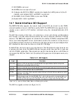
14.7.1 SI GCI Activation/Deactivation Procedure
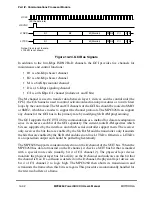
In the deactivated state, the clock pulse is disabled and the data line is at a logic one. The
layer 1 device activates the MPC8260 by enabling the clock pulses and by an indication in
the channel 0 C/I channel. The MPC8260 reports to the core (via a maskable interrupt) that
a valid indication is in the SMC RxBD.
When the core activates the line, the data output of L1TXDn is programmed to zero by
setting SI
x
GMR[STZx]. Code 0 (command timing TIM) is transmitted on channel 0 C/I
channel to the layer 1 device until STZx is reset. The physical layer device resumes the
clock pulses and gives an indication in the channel 0 C/I channel. The core should reset
STZx to enable data output.
14.7.2 Serial Interface GCI Programming
The following sections describe serial interface GCI programming.
14.7.2.1 Normal Mode GCI Programming
The user can program and conÞgure the channels used for the GCI bus interface. First, the
SI
x
MR register to the GCI/SCIT mode for that channel must be programmed, using the
DSCx, FEx, CEx, and RFSDx bits. This mode deÞnes the sync pulse to GCI sync for
framing and data clock as one-half the input clock rate. The user can program more than
one channel to interface to the GCI bus. Also, if the receive and transmit section are used
for interfacing the same GCI bus, the user internally connects the receive clock and sync
signals to the SI
x
RAM transmit section, using the CRTx bits. The user should then deÞne
the GCI frame routing and strobe select using the SI
x
RAM.
When the receive and transmit section uses the same clock and sync signals, these sections
should be programmed to the same conÞguration. Also, the L1TXDx pin in the I/O register
should be programmed to be an open-drain output. To support the monitor and the C/I
channels in GCI, those channels should be routed to one of the SMCs. To support the D
channel when there is no possibility of collision, the user should clear the SI
x
MR[GR
x
] bit
corresponding to the SCC that supports the D channel.
14.7.2.2 SCIT Programming
For interfacing the GCI/SCIT bus, SI
x
MR must be programmed to the GCI/SCIT mode.
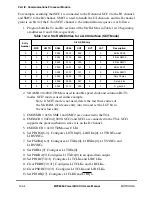
The SI
x
RAM is programmed to support a 96-bit frame length and the frame sync is
programmed to the GCI sync pulse. Generally, the SCIT bus supports the D channel access
collision mechanism. For this purpose, the user should program the CRT
x
bits so the
receive and transmit sections use the same clock and sync signals and program the GR
x
bits
to transfer the D channel grant to the SCC that supports this channel. The received (grant)
bit should be marked by programming the channel select bits of the SI
x
RAM to 0b0111
for an internal assertion of a strobe on this bit. This bit is sampled by the SI and transferred
to the D-channel SCC as the grant. The bit is generally bit 4 of the C/I in channel 2 of the
GCI, but any other bit can be selected using the SI
x
RAM.
Содержание MPC8260 PowerQUICC II
Страница 1: ...MPC8260UM D 4 1999 Rev 0 MPC8260 PowerQUICC II UserÕs Manual ª ª ...
Страница 32: ...xxxii MPC8260 PowerQUICC II UserÕs Manual MOTOROLA CONTENTS Paragraph Number Title Page Number ...
Страница 66: ...lxvi MPC8260 PowerQUICC II UserÕs Manual MOTOROLA ...
Страница 88: ...1 18 MPC8260 PowerQUICC II UserÕs Manual MOTOROLA Part I Overview ...
Страница 120: ...2 32 MPC8260 PowerQUICC II UserÕs Manual MOTOROLA Part I Overview ...
Страница 138: ...Part II iv MPC8260 PowerQUICC II UserÕs Manual MOTOROLA Part II Configuration and Reset ...
Страница 184: ...4 46 MPC8260 PowerQUICC II UserÕs Manual MOTOROLA Part II ConÞguration and Reset ...
Страница 202: ...Part III vi MPC8260 PowerQUICC II UserÕs Manual MOTOROLA Part III The Hardware Interface ...
Страница 266: ...8 34 MPC8260 PowerQUICC II UserÕs Manual MOTOROLA Part III The Hardware Interface ...
Страница 382: ...10 106 MPC8260 PowerQUICC II UserÕs Manual MOTOROLA Part III The Hardware Interface ...
Страница 392: ...11 10 MPC8260 PowerQUICC II UserÕs Manual MOTOROLA Part III The Hardware Interface ...
Страница 430: ...Part IV viii MOTOROLA Part IV Communications Processor Module ...
Страница 490: ...14 36 MPC8260 PowerQUICC II UserÕs Manual MOTOROLA Part IV Communications Processor Module ...
Страница 524: ...17 10 MPC8260 PowerQUICC II UserÕs Manual MOTOROLA Part IV Communications Processor Module ...
Страница 556: ...18 32 MPC8260 PowerQUICC II UserÕs Manual MOTOROLA Part IV Communications Processor Module ...
Страница 584: ...19 28 MPC8260 PowerQUICC II UserÕs Manual MOTOROLA Part IV Communications Processor Module ...
Страница 632: ...21 24 MPC8260 PowerQUICC II UserÕs Manual MOTOROLA Part IV Communications Processor Module ...
Страница 652: ...22 20 MPC8260 PowerQUICC II UserÕs Manual MOTOROLA Part IV Communications Processor Module ...
Страница 668: ...23 16 MPC8260 PowerQUICC II UserÕs Manual MOTOROLA Part IV Communications Processor Module ...
Страница 758: ...27 28 MPC8260 PowerQUICC II UserÕs Manual MOTOROLA Part IV Communications Processor Module ...
Страница 780: ...28 22 MPC8260 PowerQUICC II UserÕs Manual MOTOROLA Part IV Communications Processor Module ...
Страница 874: ...29 94 MPC8260 PowerQUICC II UserÕs Manual MOTOROLA Part IV Communications Processor Module ...
Страница 920: ...31 18 MPC8260 PowerQUICC II UserÕs Manual MOTOROLA Part IV Communications Processor Module ...
Страница 980: ...A 4 MPC8260 PowerQUICC II UserÕs Manual MOTOROLA Appendixes ...
Страница 1002: ...Index 22 MPC8260 PowerQUICC II UserÕs Manual MOTOROLA INDEX ...
Страница 1006: ......


