MOTOROLA
Chapter 14. Serial Interface with Time-Slot Assigner
14-19
Part IV. Communications Processor Module
6Ð7
RFSDx Receive frame sync delay for TDM a, b, c, or d. Determines the number of clock delays between the
receive sync and the Þrst bit of the receive frame. Even if CRTx is set, these bits do not control the
delay for the transmit frame.
00 No bit delay. The Þrst bit of the frame is transmitted/received on the same clock as the sync; use
for GCI.
01 1-bit delay. Use for IDL
10 2-bit delay
11 3-bit delay
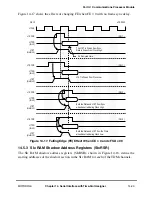
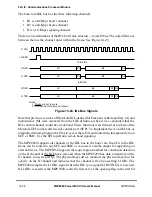
Figure 14-12 and Figure 14-13 show how these bits are used.
8
DSCx
Double speed clock for TDM a, b, c or d. Some TDMs, such as GCI, deÞne the input clock to be
twice as fast as the data rate and this bit controls this option.
0 The channel clock (L1RCLKx and/or L1TCLKx) is equal to the data clock. Use for IDL and most
TDM formats.
1 The channel clock rate is twice the data rate. Use for GCI.
9
CRTx
Common receive and transmit pins for TDM a, b, c or d. Useful when the transmit and receive
sections of a given TDM use the same clock and sync signals. In this mode, L1TCLKx and
L1TSYNCx pins can be used as general-purpose I/O pins.
0 Separate pins. The receive section of this TDM uses L1RCLKx and L1RSYNCx pins for framing
and the transmit section uses L1TCLKx and L1TSYNCx for framing.
1 Common pins. The receive and transmit sections of this TDM use L1RCLKx as clock pin of
channel x and L1RSYNCx as the receive and transmit sync pin. Use for IDL and GCI. RFSD and
TFSD are independent of one another in this mode.
10
SLx
Sync level for TDM a, b, c, or d.
0 The L1RSYNCx and L1TSYNCx signals are active on logic Ò1Ó.
1 The L1RSYNCx and L1TSYNCx signals are active on logic Ò0Ó.
11
CEx
Clock edge for TDM a, b, c or d. The function depends on DSCx.
When DSCx = 0:
0 The data is sent on the rising edge of the clock and received on the falling edge (use for IDL).
1 The data is sent on the falling edge of the clock and received on the rising edge.
When DSCx = 1:
0 The data is sent on the rising edge of the clock and received on the rising edge.
1 The data is sent on the falling edge of the clock and received on the falling edge (use for GCI).
See Figure 14-14 and Figure 14-15.
12
FEx
Frame sync edge for TDM a, b, c or d. Determines whether L1RSYNCx and L1TSYNCx pulses are
sampled with the falling/rising edge of the channel clock. See Figure 14-13, Figure 14-14,
Figure 14-15, and Figure 14-16.
0 Falling edge. Use for IDL and GCI.
1 Rising edge.
Table 14-5. SI
x
MR Field Descriptions (Continued)
Bits
Name
Description
Содержание MPC8260 PowerQUICC II
Страница 1: ...MPC8260UM D 4 1999 Rev 0 MPC8260 PowerQUICC II UserÕs Manual ª ª ...
Страница 32: ...xxxii MPC8260 PowerQUICC II UserÕs Manual MOTOROLA CONTENTS Paragraph Number Title Page Number ...
Страница 66: ...lxvi MPC8260 PowerQUICC II UserÕs Manual MOTOROLA ...
Страница 88: ...1 18 MPC8260 PowerQUICC II UserÕs Manual MOTOROLA Part I Overview ...
Страница 120: ...2 32 MPC8260 PowerQUICC II UserÕs Manual MOTOROLA Part I Overview ...
Страница 138: ...Part II iv MPC8260 PowerQUICC II UserÕs Manual MOTOROLA Part II Configuration and Reset ...
Страница 184: ...4 46 MPC8260 PowerQUICC II UserÕs Manual MOTOROLA Part II ConÞguration and Reset ...
Страница 202: ...Part III vi MPC8260 PowerQUICC II UserÕs Manual MOTOROLA Part III The Hardware Interface ...
Страница 266: ...8 34 MPC8260 PowerQUICC II UserÕs Manual MOTOROLA Part III The Hardware Interface ...
Страница 382: ...10 106 MPC8260 PowerQUICC II UserÕs Manual MOTOROLA Part III The Hardware Interface ...
Страница 392: ...11 10 MPC8260 PowerQUICC II UserÕs Manual MOTOROLA Part III The Hardware Interface ...
Страница 430: ...Part IV viii MOTOROLA Part IV Communications Processor Module ...
Страница 490: ...14 36 MPC8260 PowerQUICC II UserÕs Manual MOTOROLA Part IV Communications Processor Module ...
Страница 524: ...17 10 MPC8260 PowerQUICC II UserÕs Manual MOTOROLA Part IV Communications Processor Module ...
Страница 556: ...18 32 MPC8260 PowerQUICC II UserÕs Manual MOTOROLA Part IV Communications Processor Module ...
Страница 584: ...19 28 MPC8260 PowerQUICC II UserÕs Manual MOTOROLA Part IV Communications Processor Module ...
Страница 632: ...21 24 MPC8260 PowerQUICC II UserÕs Manual MOTOROLA Part IV Communications Processor Module ...
Страница 652: ...22 20 MPC8260 PowerQUICC II UserÕs Manual MOTOROLA Part IV Communications Processor Module ...
Страница 668: ...23 16 MPC8260 PowerQUICC II UserÕs Manual MOTOROLA Part IV Communications Processor Module ...
Страница 758: ...27 28 MPC8260 PowerQUICC II UserÕs Manual MOTOROLA Part IV Communications Processor Module ...
Страница 780: ...28 22 MPC8260 PowerQUICC II UserÕs Manual MOTOROLA Part IV Communications Processor Module ...
Страница 874: ...29 94 MPC8260 PowerQUICC II UserÕs Manual MOTOROLA Part IV Communications Processor Module ...
Страница 920: ...31 18 MPC8260 PowerQUICC II UserÕs Manual MOTOROLA Part IV Communications Processor Module ...
Страница 980: ...A 4 MPC8260 PowerQUICC II UserÕs Manual MOTOROLA Appendixes ...
Страница 1002: ...Index 22 MPC8260 PowerQUICC II UserÕs Manual MOTOROLA INDEX ...
Страница 1006: ......


