MOTOROLA
Chapter 10. Memory Controller
10-71
Part III. The Hardware Interface
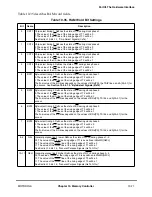
Table 10-35 describes RAM word Þelds.
Table 10-35. RAM Word Bit Settings
Bit
Name
Description
0
CST1 Chip-select timing 1. DeÞnes the state of CS during clock phase 1.
0 The value of the CS line at the rising edge of T1 will be 0
1 The value of the CS line at the rising edge of T1 will be 1
See Section 10.6.4.1.1, ÒChip-Select Signals (CxTx).Ó
1
CST2 Chip-select timing 2. DeÞnes the state of CS during clock phase 2.
0 The value of the CS line at the rising edge of T2 will be 0
1 The value of the CS line at the rising edge of T2 will be 1
2
CST3 Chip-select timing 3. DeÞnes the state of CS during clock phase 3.
0 The value of the CS line at the rising edge of T3 will be 0
1 The value of the CS line at the rising edge of T3 will be 1
3
CST4 Chip-select timing4. DeÞnes the state of CS during clock phase 4.
0 The value of the CS line at the rising edge of T4 will be 0
1 The value of the CS line at the rising edge of T4 will be 1
4
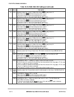
BST1
Byte-select timing 1. DeÞnes the state of BS during clock phase 1.
0 The value of the BS lines at the rising edge of T2 will be 0
1 The value of the BS lines at the rising edge of T2 will be 1
The Þnal value of the BS lines depends on the values of BRx[PS], the TSIZ lines, and A[30Ð31] for
the access. See
Section 10.6.4.1.2, ÒByte-Select Signals (BxTx)
.Ó
5
BST2
Byte-select timing 2. DeÞnes the state of BS during clock phase 2.
0 The value of the BS lines at the rising edge of T2 will be 0
1 The value of the BS lines at the rising edge of T2 will be 1
The Þnal value of the BS lines depends on the values of BRx[PS], TSIZ
x
, and A[30Ð31] for the
access.
6
BST3
Byte-select timing 3. DeÞnes the state of BS during clock phase 3.
0 The value of the BS lines at the rising edge of T3 will be 0
1 The value of the BS lines at the rising edge of T3 will be 1
The Þnal value of the BS lines depends on the values of BR
x
[PS], TSIZ
x
, and A[30Ð31] for the
access.
7
BST4
Byte-select timing 4. DeÞnes the state of BS during clock phase 4.
0 The value of the BS lines at the rising edge of T4 will be 0
1 The value of the BS lines at the rising edge of T4 will be 1
The Þnal value of the BS lines depends on the values of BRx[PS], TSIZ
x
, and A[30Ð31] for the
access.
8Ð9
G0L
General-purpose line 0 lower. DeÞnes the state of GPL0 during phases 1Ð2.
00 The value of GPL0 at the rising edge of T1 is as deÞned in M
x
MR[G0CL]
10 The value of the GPL0 line at the rising edge of T1 will be 0
11 The value of the GPL0 line at the rising edge of T1 will be 1
See Section 10.6.4.1.3, ÒGeneral-Purpose Signals (GxTx, GOx).Ó
10Ð11
G0H
General-purpose line 0 higher. DeÞnes the state of GPL0 during phase 3Ð4.
00 The value of GPL0 at the rising edge of T3 is as deÞned in M
x
MR[G0CL]
10 The value of the GPL0 line at the rising edge of T3 will be 0
11 The value of the GPL0 line at the rising edge of T3 will be 1
See Section 10.6.4.1.3, ÒGeneral-Purpose Signals (GxTx, GOx).Ó
Содержание MPC8260 PowerQUICC II
Страница 1: ...MPC8260UM D 4 1999 Rev 0 MPC8260 PowerQUICC II UserÕs Manual ª ª ...
Страница 32: ...xxxii MPC8260 PowerQUICC II UserÕs Manual MOTOROLA CONTENTS Paragraph Number Title Page Number ...
Страница 66: ...lxvi MPC8260 PowerQUICC II UserÕs Manual MOTOROLA ...
Страница 88: ...1 18 MPC8260 PowerQUICC II UserÕs Manual MOTOROLA Part I Overview ...
Страница 120: ...2 32 MPC8260 PowerQUICC II UserÕs Manual MOTOROLA Part I Overview ...
Страница 138: ...Part II iv MPC8260 PowerQUICC II UserÕs Manual MOTOROLA Part II Configuration and Reset ...
Страница 184: ...4 46 MPC8260 PowerQUICC II UserÕs Manual MOTOROLA Part II ConÞguration and Reset ...
Страница 202: ...Part III vi MPC8260 PowerQUICC II UserÕs Manual MOTOROLA Part III The Hardware Interface ...
Страница 266: ...8 34 MPC8260 PowerQUICC II UserÕs Manual MOTOROLA Part III The Hardware Interface ...
Страница 382: ...10 106 MPC8260 PowerQUICC II UserÕs Manual MOTOROLA Part III The Hardware Interface ...
Страница 392: ...11 10 MPC8260 PowerQUICC II UserÕs Manual MOTOROLA Part III The Hardware Interface ...
Страница 430: ...Part IV viii MOTOROLA Part IV Communications Processor Module ...
Страница 490: ...14 36 MPC8260 PowerQUICC II UserÕs Manual MOTOROLA Part IV Communications Processor Module ...
Страница 524: ...17 10 MPC8260 PowerQUICC II UserÕs Manual MOTOROLA Part IV Communications Processor Module ...
Страница 556: ...18 32 MPC8260 PowerQUICC II UserÕs Manual MOTOROLA Part IV Communications Processor Module ...
Страница 584: ...19 28 MPC8260 PowerQUICC II UserÕs Manual MOTOROLA Part IV Communications Processor Module ...
Страница 632: ...21 24 MPC8260 PowerQUICC II UserÕs Manual MOTOROLA Part IV Communications Processor Module ...
Страница 652: ...22 20 MPC8260 PowerQUICC II UserÕs Manual MOTOROLA Part IV Communications Processor Module ...
Страница 668: ...23 16 MPC8260 PowerQUICC II UserÕs Manual MOTOROLA Part IV Communications Processor Module ...
Страница 758: ...27 28 MPC8260 PowerQUICC II UserÕs Manual MOTOROLA Part IV Communications Processor Module ...
Страница 780: ...28 22 MPC8260 PowerQUICC II UserÕs Manual MOTOROLA Part IV Communications Processor Module ...
Страница 874: ...29 94 MPC8260 PowerQUICC II UserÕs Manual MOTOROLA Part IV Communications Processor Module ...
Страница 920: ...31 18 MPC8260 PowerQUICC II UserÕs Manual MOTOROLA Part IV Communications Processor Module ...
Страница 980: ...A 4 MPC8260 PowerQUICC II UserÕs Manual MOTOROLA Appendixes ...
Страница 1002: ...Index 22 MPC8260 PowerQUICC II UserÕs Manual MOTOROLA INDEX ...
Страница 1006: ......

