MOTOROLA
Chapter 12. IEEE 1149.1 Test Access Port
12-29
Part III. The Hardware Interface
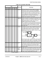
Table 12-3. Instruction Decoding
Code
Instruction
Description
B7
B6
B5
B4
B3
B2
B1
B0
0
0
0
0
0
0
0
0
EXTEST
External test. Selects the 475-bit boundary scan register.
EXTEST also asserts an internal reset for the MPC8260Õs
system logic to force a known beginning internal state while
performing external boundary scan operations. By using the
TAP, the register is capable of scanning user-deÞned values
into the output buffers, capturing values presented to input pins,
and controlling the output drive of three-state output or
bidirectional pins. For more details on the function and use of
EXTEST, refer to the IEEE 1149.1 standard.
1
1
0
0
0
0
0
0
SAMPLE/
PRELOAD
Initializes the boundary scan register output cells before the
selection of EXTEST. This initialization ensures that known data
appears on the outputs when entering an EXTEST instruction.
SAMPLE/PRELOAD also provides a chance to obtain a
snapshot of system data and control signals.
NOTE: Since there is no internal synchronization between the
TCK and CLKOUT, the user must provide some form of external
synchronization between the JTAG operation at TCK frequency
and the system operation CLKOUT frequency to achieve
meaningful results.
1
1
1
1
1
1
1
1
BYPASS
The BYPASS instruction creates a shift register path from TDI
to the bypass register and, Þnally, to TDO, circumventing the
475-bit boundary scan register. This instruction is used to
enhance test efÞciency when a component other than the
MPC8260 becomes the device under test. It selects the single-
bit bypass register as shown below.
When the bypass register is selected by the current instruction,
the shift register stage is cleared on the rising edge of TCK in
the capture-DR controller state. Thus, the Þrst bit to be shifted
out after selecting the bypass register is always a logic zero.
1
1
1
1
0
0
0
0
HIÐZ
Provided as a manufacturerÕs optional public instruction to avoid
back driving the output pins during circuit-board testing. When
HI-Z is invoked all output drivers, including the two-state
drivers, are turned off (high impedance). The instruction selects
the bypass register.
1
1
1
1
0
0
0
1
CLAMP
and
BYPASS
CLAMP selects the single-bit bypass register as shown in the
BYPASS instruction Þgure above, and the state of all signals
driven from the system output pins is completely deÞned by the
data previously shifted into the boundary scan register. For
example, using the SAMPLE/PRELOAD instruction.
B0 (lsb) is shifted Þrst.
1
1
MUX
G1
C
D
To TDO
From TDI
0
Shift DR
Clock DR
Содержание MPC8260 PowerQUICC II
Страница 1: ...MPC8260UM D 4 1999 Rev 0 MPC8260 PowerQUICC II UserÕs Manual ª ª ...
Страница 32: ...xxxii MPC8260 PowerQUICC II UserÕs Manual MOTOROLA CONTENTS Paragraph Number Title Page Number ...
Страница 66: ...lxvi MPC8260 PowerQUICC II UserÕs Manual MOTOROLA ...
Страница 88: ...1 18 MPC8260 PowerQUICC II UserÕs Manual MOTOROLA Part I Overview ...
Страница 120: ...2 32 MPC8260 PowerQUICC II UserÕs Manual MOTOROLA Part I Overview ...
Страница 138: ...Part II iv MPC8260 PowerQUICC II UserÕs Manual MOTOROLA Part II Configuration and Reset ...
Страница 184: ...4 46 MPC8260 PowerQUICC II UserÕs Manual MOTOROLA Part II ConÞguration and Reset ...
Страница 202: ...Part III vi MPC8260 PowerQUICC II UserÕs Manual MOTOROLA Part III The Hardware Interface ...
Страница 266: ...8 34 MPC8260 PowerQUICC II UserÕs Manual MOTOROLA Part III The Hardware Interface ...
Страница 382: ...10 106 MPC8260 PowerQUICC II UserÕs Manual MOTOROLA Part III The Hardware Interface ...
Страница 392: ...11 10 MPC8260 PowerQUICC II UserÕs Manual MOTOROLA Part III The Hardware Interface ...
Страница 430: ...Part IV viii MOTOROLA Part IV Communications Processor Module ...
Страница 490: ...14 36 MPC8260 PowerQUICC II UserÕs Manual MOTOROLA Part IV Communications Processor Module ...
Страница 524: ...17 10 MPC8260 PowerQUICC II UserÕs Manual MOTOROLA Part IV Communications Processor Module ...
Страница 556: ...18 32 MPC8260 PowerQUICC II UserÕs Manual MOTOROLA Part IV Communications Processor Module ...
Страница 584: ...19 28 MPC8260 PowerQUICC II UserÕs Manual MOTOROLA Part IV Communications Processor Module ...
Страница 632: ...21 24 MPC8260 PowerQUICC II UserÕs Manual MOTOROLA Part IV Communications Processor Module ...
Страница 652: ...22 20 MPC8260 PowerQUICC II UserÕs Manual MOTOROLA Part IV Communications Processor Module ...
Страница 668: ...23 16 MPC8260 PowerQUICC II UserÕs Manual MOTOROLA Part IV Communications Processor Module ...
Страница 758: ...27 28 MPC8260 PowerQUICC II UserÕs Manual MOTOROLA Part IV Communications Processor Module ...
Страница 780: ...28 22 MPC8260 PowerQUICC II UserÕs Manual MOTOROLA Part IV Communications Processor Module ...
Страница 874: ...29 94 MPC8260 PowerQUICC II UserÕs Manual MOTOROLA Part IV Communications Processor Module ...
Страница 920: ...31 18 MPC8260 PowerQUICC II UserÕs Manual MOTOROLA Part IV Communications Processor Module ...
Страница 980: ...A 4 MPC8260 PowerQUICC II UserÕs Manual MOTOROLA Appendixes ...
Страница 1002: ...Index 22 MPC8260 PowerQUICC II UserÕs Manual MOTOROLA INDEX ...
Страница 1006: ......

