


Phase-Locked Loop and Clock Dividers
MCF5253 Reference Manual, Rev. 1
4-6
Freescale Semiconductor
4.3
Dynamic Clock Switching
The Glitch-free Clock Rate divider block works on the PDM (Pulse Density Modulation) principal. As it
is a divider, it only reduces the clock rate output from the PLL module. It does this by gating out
(removing) clock pulses to reach the desired clock rate (operating frequency). This implies that clock
pulses after the Clock Rate divider block may not be equi-distant depending on the chosen divider value.
The re-action time of the Clock Rate divider block is in the order of 20nS.
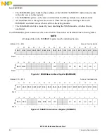
The Clock Rate divider block is controlled by a 32-bit register as shown in
NOTE
Do not make the PLL output frequency any higher than required for the
actual application. The higher the PLL operating frequency then the higher
the power consumption of the PLL block.
4.4
Audio Clock Generation
The audio clocks and output DAC clocks are derived directly from the CRIN pin. Clock settings depend
on CRSEL, CLSEL, and AUDIOSEL bits, as explained in
AUDIO_CLOCK is completely derived from the AUDIOSEL bit, and this clock is independent of the
other select bits. For the DAC clocks (MCLK2 and MCLK1) the relationship between CRSEL and CLSEL
is defined in
Offset: MB 0x170
Access: User read/write
31
30
29
28
27
26
25
24
23
22
21
20
19
18
17
16
15
14
13
12
11
10
9
8
7
6
5
4
3
2
1
0
R 0
0
0
0
0
0
0
0
0
0
0
0
0
0
0
0
0
0
0
0
0
0
0
0
Clock rate select
W
Reset 0
0
0
0
0
0
0
0
0
0
0
0
0
0
0
0
0
0
0
0
0
0
0
0
1
1
1
1
1
1
1
1
Figure 4-3. ClockRate Register
Table 4-6. ClockRate Field Descriptions
Field
Description
31–8
Reserved, should be cleared.
7–0
Clock Rate
Select
Sets the divider to pass-thru mode and no clock rate reduction is applied. At reset, this bit field is set to 0xFF.
Clock Rate Select = round ((Desired Clock Rate / PLL Output Frequency)
×
255)
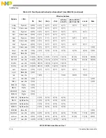
Table 4-7. PLLCR Bit Fields
PLLCR[CLSEL]
(Bits 30–28)
PllCR CRsel
(Bit 23)
pllCR Config
Audiosel
(Bit 22)
AUDIO_CLOCK
MCLK2
MCLK1
000
1
1
CRIN
CRIN
CRIN/2
001
1
1 CRIN
CRIN
CRIN
010
1
1
CRIN
CRIN/2
CRIN/2
Summary of Contents for MCF5253
Page 1: ...Document Number MCF5253RM Rev 1 08 2008 MCF5253 Reference Manual...
Page 26: ...MCF5253 Reference Manual Rev 1 xxvi Freescale Semiconductor...
Page 32: ...MCF5253 Reference Manual Rev 1 xxxii Freescale Semiconductor...
Page 46: ...MCF5253 Introduction MCF5253 Reference Manual Rev 1 1 14 Freescale Semiconductor...
Page 62: ...Signal Description MCF5253 Reference Manual Rev 1 2 16 Freescale Semiconductor...
Page 98: ...Instruction Cache MCF5253 Reference Manual Rev 1 5 10 Freescale Semiconductor...
Page 104: ...Static RAM SRAM MCF5253 Reference Manual Rev 1 6 6 Freescale Semiconductor...
Page 128: ...Synchronous DRAM Controller Module MCF5253 Reference Manual Rev 1 7 24 Freescale Semiconductor...
Page 144: ...Bus Operation MCF5253 Reference Manual Rev 1 8 16 Freescale Semiconductor...
Page 176: ...System Integration Module SIM MCF5253 Reference Manual Rev 1 9 32 Freescale Semiconductor...
Page 198: ...Analog to Digital Converter ADC MCF5253 Reference Manual Rev 1 12 6 Freescale Semiconductor...
Page 246: ...DMA Controller MCF5253 Reference Manual Rev 1 14 18 Freescale Semiconductor...
Page 282: ...UART Modules MCF5253 Reference Manual Rev 1 15 36 Freescale Semiconductor...
Page 344: ...Audio Interface Module AIM MCF5253 Reference Manual Rev 1 17 46 Freescale Semiconductor...
Page 362: ...I2 C Modules MCF5253 Reference Manual Rev 1 18 18 Freescale Semiconductor...
Page 370: ...Boot ROM MCF5253 Reference Manual Rev 1 19 8 Freescale Semiconductor...


