


System Integration Module (SIM)
MCF5253 Reference Manual, Rev. 1
9-28
Freescale Semiconductor
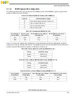
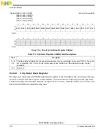
At power-on, the function is always the primary function. When a ‘0’ is programmed in any bit of
GPIO-FUNCTION or GPIO1-FUNCTION, the corresponding pin gets its primary function. In this case,
output drive strength and output value are determined by the primary function logic. When a ‘1’ is
programmed the corresponding pin is in GPO-mode, drive direction is determined by value in GPIO-EN
or GPIO1-EN. When a ‘0’ is programmed in any bit, the corresponding pin is driven to high-impedance
state. When a ‘1’ is programmed, the corresponding pin is driven low or high.
When a pin is in GPO-mode, and being driven low-impedance, the actual drive value of the pin is
determined by what is programmed in the corresponding bit of registers GPIO-OUT
or
GPIO1-OUT. If
‘0’ is programmed here, the pin is driven low. If ‘1’ is programmed, the pin is driven high.
Figure 9-15. General-Purpose Pin Logic for Pin SCLK3/GPIO35
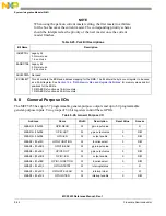
Table 9-29. General-Purpose Output Register Bits to Pins Mapping
GPIO-Function
GPIO-EN
GPIO-OUT
Bit Number
Associated Pin
Pin Type
GPIO1-Function
GPIO1-EN
GPIO1-OUT
Bit Number
Associated Pin
Pin Type
31
IDE_DIOR/GPIO31
I/O
63
BCLKE/GPIO63
I/O
30
BUFENB2/GPIO30
I/O
62
none
I/O
29
BUFENB1/GPIO29
I/O
61
none
I/O
28
CS1/QSPICS3/GPIO28
I/O
60
SD_CS0/GPIO60
I/O
27
QSPIDOUT/SFSY/GPIO27
I/O
59
SDRAS/GPIO59
I/O
26
RCK/QSPIDIN/QSPI
DOUT/GPIO26
I/O
58
ADOUT/SCLK4/GPIO58
I/O
25
QSPICLK/SUBR/GPIO25
I/O
57
none
I/O
24
QSPICS2/MCLK2/GPIO24
I/O
56
none
I/O
23
LRCK2/GPIO23
I/O
55
none
I/O
22
SCLK2/GPIO22
I/O
54
A23/GPO54
O
21
WAKEUP/GPIO21
I/O
53
SDUDQM/GPO53
O
20
SCLK1/GPIO20
I/O
52
SDLDQM/GPO52
O
19
LRCK1/GPIO19
I/O
51
PSTCLK/GPIO51
I/O
18
SDATAO1/TOUT0/GPIO18
I/O
50
PST0/GPIO50
I/O
17
SDATAI1/GPIO17
I/O
49
PST1/GPIO49
I/O
GPIO1-READ
SCLK3 Input Value
SCLK3 Drive Value
GPIO1-OUT
SCLK3 Drive Strength
GPIO1-EN
GPIO1-FUNCTION
0
1
0
1
SCLK3/GPIO35
Summary of Contents for MCF5253
Page 1: ...Document Number MCF5253RM Rev 1 08 2008 MCF5253 Reference Manual...
Page 26: ...MCF5253 Reference Manual Rev 1 xxvi Freescale Semiconductor...
Page 32: ...MCF5253 Reference Manual Rev 1 xxxii Freescale Semiconductor...
Page 46: ...MCF5253 Introduction MCF5253 Reference Manual Rev 1 1 14 Freescale Semiconductor...
Page 62: ...Signal Description MCF5253 Reference Manual Rev 1 2 16 Freescale Semiconductor...
Page 98: ...Instruction Cache MCF5253 Reference Manual Rev 1 5 10 Freescale Semiconductor...
Page 104: ...Static RAM SRAM MCF5253 Reference Manual Rev 1 6 6 Freescale Semiconductor...
Page 128: ...Synchronous DRAM Controller Module MCF5253 Reference Manual Rev 1 7 24 Freescale Semiconductor...
Page 144: ...Bus Operation MCF5253 Reference Manual Rev 1 8 16 Freescale Semiconductor...
Page 176: ...System Integration Module SIM MCF5253 Reference Manual Rev 1 9 32 Freescale Semiconductor...
Page 198: ...Analog to Digital Converter ADC MCF5253 Reference Manual Rev 1 12 6 Freescale Semiconductor...
Page 246: ...DMA Controller MCF5253 Reference Manual Rev 1 14 18 Freescale Semiconductor...
Page 282: ...UART Modules MCF5253 Reference Manual Rev 1 15 36 Freescale Semiconductor...
Page 344: ...Audio Interface Module AIM MCF5253 Reference Manual Rev 1 17 46 Freescale Semiconductor...
Page 362: ...I2 C Modules MCF5253 Reference Manual Rev 1 18 18 Freescale Semiconductor...
Page 370: ...Boot ROM MCF5253 Reference Manual Rev 1 19 8 Freescale Semiconductor...